

 Manufacturers
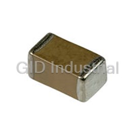
BCCOMPONENTS/VISHAY VJ0402V103ZXJCW1BC

Description
CAP 10000PF 16V CERAMIC Y5V 0402
Part Number
VJ0402V103ZXJCW1BC
Price
Request Quote
Manufacturer
BCCOMPONENTS/VISHAY
Lead Time
Request Quote
Category
PRODUCTS - V
Datasheet

Extracted Text
Class 3 Y5V 10/16/25/50/100 V Vishay BCcomponents Surface Mount Multilayer Chip Capacitors FEATURES • Class 3 dielectric • Four standard sizes • High capacitance per unit volume • Supplied in tape on reel • For high frequency applications • Ni-barrier with 100 % tin terminations. APPLICATIONS • Consumer electronics • Telecommunications • Data processing GENERAL SPECIFICATIONS • Mobile applications NOTE: Electrical characteristics values - temperature at 20 ± 1 °C, pressure at 86 to 106 Kpa and Temperature Coefficient: humidity at 63 to 67 % unless otherwise stated Rated Voltage U (DC): 10 V; 16 V; 25 V; 50 V; 100 V + 30/ - 80% R Capacitance Range: 0.01 µF to 10 µF Insulation Resistance after 120 seconds at UR (DC): Tolerance on Capacitance: R 10 GΩ minimum or 500ΩF mininimum, whichever is less ins After 1000 hours; ± 20 %; - 20/+ 80% Climatic Category (IEC 68): 25/85/21 Tan δδδδ: Test Voltage (DC) for 1 minute: 2.5 x U R Ageing: typical 7 % per time decade see Tests and requirements DIMENSIONS in inches [millimeters] SIZE T LW MB CODE MAX. 0.040 ± 0.002 0.020 ± 0.002 0.022 0.010 + 0.002/- 0.004 0402 [1.0 ± 0.05] [0.5 ± 0.05] [0.55] [0.25 + 0.05/− 0.0.1] 0.063 ± 0.004 0.030 ± 0.004 0.035 0.015 ± 0.006 W T 0603 [1.6 ± 0.10] [0.8 ± 0.07] [0.87] [0.40 ± 0.15] 0.080 ± 0.006 0.050 ± 0.006 0.053 0.020 ± 0.008 MB MB 0805 [2.0 ± 0.15] [1.25 ± 0.15] [1.35] [0.50 ± 0.20] L 0.125 ± 0.006 0.063 ± 0.006 0.069 0.025 ± 0.008 1206 [3.2 ± 0.15] [1.6 ± 0.15] [1.80] [0.60 ± 0.20] ORDERING INFORMATION VJ0402 V 103 M X Q C W1BC SIZE CODE DIELECTRIC CAPACITANCE TOLERANCE TERMINATION VOLTAGE PACKAGING TECHNOLOGY 0402 V = Y5V two signiŢcant digits M = ± 20 % X = Ni-Barrier Q = 10 V C = 7 inch followed by the reel/paper 0603 Z = - 20/+ 80 % J = 16 V number of zeros: P = 13 inch 0805 X = 25 V 103 = 10000 reel/paper 1206 A = 50 V T = 7 inch B = 100 V reel/blister R = 13 inch reel/blister www.vishay.com For technical questions contact MLCC@vishay.com Document Number 28505 22 Revision 01-Dec-03 Class 3 Y5V 10/16/25/50/100 V Vishay BCcomponents Surface Mount Multilayer Chip Capacitors SELECTION CHART FOR 10/16/25/50 AND 100 V DIELECTRIC Y5V EIA CAP SIZE 0402 0603 0805 1206 CODE VDC W 10 V 16 V 25 V 50 V 100 V 10 V 16 V 25 V 50 V 100 V 10 V 16 V 25 V 50 V 100 V 10 V 16 V 25 V 50 V 100 V 102 1000 pF 122 1200 152 1500 182 1800 222 2200 272 2700 332 3300 392 3900 472 4700 562 5600 682 6800 822 8200 103 N N N N SSSS AAAA B BBBB B 0.01 µF 123 N N N N SSSS AAAA BBBB 0.012 153 N N N N SSSS AAAA B BBBB B 0.015 183 N N N N SSSS AAAA BBBB 0.018 223 N N N N SSSS AAAA B BBBB B 0.022 273 N N N N SSSS AAAA BBBB 0.027 333 N N N N SSSS AAAA B BBBB B 0.033 393 N N N SSSS AAAA BBBB 0.039 473 N N N SSSS AAAA B BBBB B 0.047 563 N N SSSS AAAA BBBB 0.056 683 N N SSSS AAAA B BBBB B 0.068 823 N N SSSS AAAA BBBB 0.082 104 N N SSSS AAAA B BBBB B 0.1 µF 154 N SSSS AAAA BBBB C 0.15 224 N SSS AAAA BBBB C 0.22 334 SSS BBBB BBBB 0.33 474 SS BBB BBBB 0.47 684 S B B D BBBB 0.68 105 S B B D CCCC 1 µF 155 DD CCC 1.5 225 DD CCC 2.2 335 DDDD 3.3 475 DDD 4.7 685 D 6.8 106 D 10 µF 226 22 µF Document Number 28505 For technical questions contact MLCC@vishay.com www.vishay.com Revision 01-Dec-03 23 Class 3 Y5V 10/16/25/50/100 V Vishay BCcomponents Surface Mount Multilayer Chip Capacitors PACKAGING QUANTITIES THICKNESS AMOUNT PER REEL CLASSIFICATION ∆∆ ∆∆180 mm; 7 inch (mm) 0402 0603 0805 1206 A = 0.6 ± 0.1 - - Paper 4 Kp/Reel - B = 0.8 ± 0.1 - - Paper 4 Kp/Reel Paper 4 Kp/Reel C = 0.95 ± 0.1 - - - Plastic 3 Kp/Reel D = 1.25 ± 0.1 - - Plastic 3 Kp/Reel Plastic 3 Kp/Reel G = 1.60 ± 0.2 - - - Plastic 2 Kp/Reel S = 0.8 ± 0.07 - Paper 4 Kp/Reel - - N = 0.50 ± 0.05 Paper 10 Kp/Reel - - - K = 2.00 ± 0.2 ---- M = 2.5 ± 0.30 ---- PACKAGING QUANTITIES AMOUNT PER REEL THICKNESS CLASSIFICATION ∆∆∆∆330 mm; 13 inch (mm) 0402 0603 0805 1206 A = 0.6 ± 0.1 - - Paper 15 Kp/Reel - B = 0.8 ± 0.1 - - Paper 15 Kp/Reel Paper 15 Kp/Reel C = 0.95 ± 0.1 - - - Plastic 10 Kp/Reel D = 1.25 ± 0.1 - - Plastic 10 Kp/Reel Plastic 10 Kp/Reel G = 1.60 ± 0.2 ---- S = 0.8 ± 0.07 - Paper 15 Kp/Reel - - N = 0.50 ± 0.05 Paper 50 Kp/Reel - - - K = 2.00 ± 0.2 ---- M = 2.5 ± 0.30 ---- COVER TAPE (POLYESTER - ANTISTATIC) CARRIER TAPE (POLYCARBONATE) PROPERTIES OF COVER TAPE PROPERTIES OF CARRIER TAPE WIDTH WIDTH PARAMETER PARAMETER 5.5 ± ± ± ± 0.1 mm 8.1 ± ± ± ± 0.2 mm Breaking force ≥ 10.7 N Thickness 190 to 280 µm 2 Elongation at break ≥ 63 % Tensile strength at break > 60 N /mm 10 Surface resistance < 10 Ω /sq. Elongation at break 100 to 150 % 12 Softening point 71 ± 5 °C Surface resistance > 10 Ω /sq. Thickness 62 µm PAPER TAPE SPECIFICATIONS DIMENSIONS OF PAPER TAPE in millimeters T 1 P 0 PRODUCT SIZE CODE P D 2 0 SYMBOL 0402 0603 0805 1206 SIZE TOL. SIZE TOL. SIZE TOL. SIZE TOL. E A 0.62 ± 0.05 1.02 ± 0.05 1.50 ± 0.10 2.00 ± 0.15 0 B 1.12 ± 0.05 1.82 ± 0.05 2.30 ± 0.10 3.50 ± 0.15 0 F W W 8.00 ± 0.10 8.00 ± 0.10 8.00 ± 0.10 8.00 ± 0.10 B 0 E 1.75 ± 0.10 1.75 ± 0.10 1.75 ± 0.10 1.75 ± 0.10 F 3.50 ± 0.05 3.50 ± 0.05 3.50 ± 0.05 3.50 ± 0.05 D 1.55 ± 0.05 1.55 ± 0.05 1.55 ± 0.05 1.55 ± 0.05 0 P 4.00 ± 0.10 4.00 ± 0.10 4.00 ± 0.10 4.00 ± 0.10 A 0 0 P 1 P 2.00 ± 0.05 4.00 ± 0.10 4.00 ± 0.10 4.00 ± 0.10 1 T 2 P 2.00 ± 0.05 2.00 ± 0.05 2.00 ± 0.05 2.00 ± 0.05 2 www.vishay.com For technical questions contact MLCC@vishay.com Document Number 28505 24 Revision 01-Dec-03 Class 3 Y5V 10/16/25/50/100 V Vishay BCcomponents Surface Mount Multilayer Chip Capacitors BLISTER TAPE SPECIFICATIONS DIMENSIONS OF BLISTER TAPE in millimeters K P 0 0 PRODUCT T D P 2 DIMENSION TOLERANCE 0 0805 1206 A < 1.55 < 2.00 - E 0 B < 2.45 < 3.60 - 0 W 8.00 8.00 ± 0.20 F cover tape W E 1.75 1.75 ± 0.10 F 3.50 3.50 ± 0.05 B 0 D 1.50 1.50 + 0.10/ - 0 0 D 1.00 1.00 ± 0.10 1 P 4.00 4.00 ± 0.05 0 T A D 1 0 1 P 4.00 4.00 ± 0.10 direction of unreeling 1 T P 2 1 P 2.00 2.00 ± 0.05 2 REEL SPECIFICATIONS DC A B REEL DIMENSIONS AND TAPE WIDTH in millimeters ∅∅ ∅∅ ∅∅ 180 mm; 7 inch ∅∅ 330 mm; 13 inch A 13.0 ± 1.0 13.0 ± 0.5 B 9.0 ± 1.0 9.0 ± 0.5 C 178.0 ± 1.0 330.0 ± 1.0 D 60.5 ± 1.0 100.0 ± 1.0 METHOD OF MOUNTING AND DIMENSIONS OF SOLDER LANDS For normal use the capacitors may be mounted on printed-circuit boards or ceramic substrates by applying wave soldering and reflow soldering. An improper combination of soldering, substrate and chip size can lead to a damaging of the component. The risk increases with the chip size and with temperature fluctuations (> 100 °C) Therefore, it is advised to use the smallest possible size and follow the dimensional recommendations given. Document Number 28505 For technical questions contact MLCC@vishay.com www.vishay.com Revision 01-Dec-03 25 Class 3 Y5V 10/16/25/50/100 V Vishay BCcomponents Surface Mount Multilayer Chip Capacitors SOLDERING GRAPHS IR REFLOW WITH SnPb SOLDER IR REFLOW WITH SnAgCu SOLDER 300 300 Max temperature T T (°C) (°C) Max temperature 250 250 > 215°C: 20 ~ 40 seconds 200 200 Sn-Ag-Cu solder paste 150 150 Min temperature Min temperature 100 100 Sn-Pb Eutectic solder paste 50 50 0 0 30 ~ 60 sec time time 60 ~ 120 seconds 60 ~ 120 seconds 60 ~ 120 seconds 30 ~ 60 seconds 30 ~ 60 seconds 30 ~ 60 seconds WAVE SOLDERING REFLOW SOLDERING 300 300 10 s 10 s T T (°C) 260 °C (°C) 245 °C 250 250 235 °C to 260 °C second wave 10 s 215 °C 200 200 5 K/s first wave 40 s 180 °C 2 K/s 200 K/s 150 150 130 °C 100 °C to 130 °C forced 100 100 cooling 2 K/s 2 K/s 50 50 0 0 0 50 100 150 200 250 0 50 100 150 200 250 t (s) t (s) RECOMMENDED DIMENSIONS OF SOLDER LANDS in millimeters solder land / solder paste pattern solder resist DG pattern occupied area E C B A tracks F www.vishay.com For technical questions contact MLCC@vishay.com Document Number 28505 26 Revision 01-Dec-03 preferred direction during wave soldering Class 3 Y5V 10/16/25/50/100 V Vishay BCcomponents Surface Mount Multilayer Chip Capacitors REFLOW SOLDERING FOOTPRINT DIMENSIONS in mm SIZE PLACEMENT PROCESSING REMARKS CODE ACCURACY AB CD E F G 0402 1.50 0.50 0.50 0.50 0.10 1.75 0.95 ± 0.15 0603 2.30 0.70 0.80 0.80 0.20 2.55 1.40 ± 0.25 IR or hot plate soldering 0805 2.80 1.00 0.90 1.30 0.40 3.08 1.85 ± 0.25 1206 4.00 2.20 0.90 1.60 1.60 4.25 2.25 ± 0.25 WAVE SOLDERING FOOTPRINT DIMENSIONS in mm PROPOSED NUMBER AND DIMENSIONS PLACEMENT SIZE OF DUMMY TRACKS ACCURACY CODE A BCD E F G (mm) (mm) 0603 2.40 1.00 0.70 0.80 0.20 3.10 1.90 1 x (0.2 x 0.8) ± 0.10 0805 3.20 1.40 0.90 1.30 0.36 4.10 2.50 1 x (0.3 x 1.3) ± 0.15 1206 4.80 2.30 1.25 1.70 1.25 5.90 3.20 3 x (0.25 x 1.7) ± 0.25 TEST CONDITIONS IN STATIC SOLDER BATH PARAMETER DESCRIPTION SOLDERABILITY CECC requirement: 235 ± 5 °C for 2 ± 0.5 seconds 95 % covered with smooth and bright solder coating IEC requirement: 215 ± 3 °C for 3 ± 0.3 seconds RESISTANCE TO LEACHING 10 % of the metallization of the edges of the head face may be missing 260 ± 5 °C for 30 ± 1 second (inner electrodes are not visible) TESTS AND REQUIREMENTS TESTS PROCEDURES AND REQUIREMENTS TEST PROCEDURE REQUIREMENTS Visual and no visible damage dimensions in accordance mechanical with speciŢcation C ≤ 10 µF; 1.0 ± 0.2 Vrms; 1 kHz ± 10 % shall not exceed the limits given in the detailed Capacitance speciŢcation C > 10 µF; 0.5 ± 0.2 Vrms; 120 kHz ± 20 % DF: ≤ 5.0 %: 50 V, 25 V (except 0603 ≥ 0.1 µF; 0805 ≥ 0.33 µF; C ≤ 10 µF; 1.0 ± 0.2 Vrms; 1 kHz ± 10 % Dissipation factor 1206 ≥ 0.1 µF, ≤ 7.0 %) C > 10 µF; 0.5 ± 0.2 Vrms; 120 kHz ± 20 % ≤ 7.0 % (C < 1.0 µF, 16 V); ≤ 9.0 % (C ≥ 1.0 µF, 16 V); ≤ 12.5 % (10 V) 250 % of rated voltage for 1 to 5 seconds, charge and discharge Dielectric strength no visible damage or ţash-over during test current less than 50 mA 10 GΩ minimum or 500 ΩF minimum, Insulation resistance at U (DC) for maximum 120 seconds R whichever is less Temperature with no electrical load: within + 30/− 80% coefŢcient − 25 to 85 °C at T = 20 °C amb no visible damage the middle part of the substrate shall be pressurized by means of ∆C/C: ≤ ± 30 % the pressurizing rod at a rate of about 1 mm per second until the this capacitance change means the change of Bending test deţection becomes 1 mm and then the pressure shall be capacitance under speciŢed ţexure of maintained for 5 ± 1 second; measurement after 48 ± 4 hours at substrate from the capacitance measured room temperature before the test Document Number 28505 For technical questions contact MLCC@vishay.com www.vishay.com Revision 01-Dec-03 27 Class 3 Y5V 10/16/25/50/100 V Vishay BCcomponents Surface Mount Multilayer Chip Capacitors TESTS PROCEDURES AND REQUIREMENTS TEST PROCEDURE REQUIREMENTS 95 % minimum coverage of entire Solderability 230 ± 5 °C for 2 ± 0.5 seconds; Solder: SN63A metallized area Solder temperature: 260 ± 5 °C Dipping time: 10 ± 1 seconds no visible damage Solder: SN63A Resistance to Before initial measurement: Perform 150 + 0/ - 10 °C for 1 hour ∆C/C: ≤ ± 20 % and then set for 48 ± 4 hours at room temperature. soldering heat DF, R and dielectric strength to meet initial ins Preheating: 120 to 150 °C for 1 minute before immerse the requirements capacitor in a eutectic solder. Measurement to be made after 48 ± 4 hours at room temperature Test temperature − 55 to 85 °C: no visible damage − 55 °C − 3/+ 0 °C for 30 ± 3 minutes; Room temperature for 2 to 3 minutes; ∆C/C: ≤ ± 20 % Temperature cycle X5R: 85 °C + 3/− 0 °C for 30 ± 3 minutes; DF, R and dielectric strength to meet initial ins Room temperature for 2 to 3 minutes requirements Measurement to be made after 48 ± 4 hours at room temperature ∆C/C: ≤ ± 30 % DF: ≤ 7.5 % U (DC): ≥ 50 V, 25 V R Test temperature: 40 ± 2 °C (except 0603 ≥ 0.1 µF; Humidity test Humidity: 90 to 95 % RH 0805 ≥ 0.33 µF; 1206 ≥ 1 µF, ≤ 10 %) (damp heat steady Test time: 500 + 24/− 0 hours ≤ 10 % (C < 1.0 µF, 16 V); state) Measurement to be made after 48 ± 4 hours at room temperature ≤ 12.5 % (C ≥ 1.0 µF, 16 V; 0402 ≥ 0.068 µF) ≤ 15 % (10 V) R : 1 GΩ minimum or 50 ΩF minimum, ins whichever is less no visual damage ∆C/C: ± 30 % DF: Test temperature: 40 ± 2 °C ≤ 7.5 % U (DC): ≥ 50 V, 25 V R Humidity: 90 to 95 % RH (except 0603 ≥ 0.1 µF; Humidity load Test time: 500 + 24/− 0 hours 0805 ≥ 0.33 µF; 1206 ≥ 1 µF, ≤ 10 %) (damp heat) To apply voltage: rated voltage ≤ 10 % (C < 1.0 µF, 16 V); Measurement to be made after 48 ± 2 hours at room temperature ≤ 12.5 % (C ≥ 1.0 µF, 16 V; 0402 ≥ 0.068 µF) ≤ 15 % (10 V) R : 500 MΩ minimum or 25 ΩF minimum, ins whichever is less Adhesive strength of Pressurizing force 5 N (≤ 0603) and 10 N (> 0603) no visible damage termination Test time10 ± 1 second Vibration frequency: 10 to 55 Hz/minute; Total amplitude: 1.5 mm no visible damage or removal of the Vibration resistance Test time: 6 hours (2 hours each in 3 mutually perpendicular terminations directions) no visual damage ∆C/C: ≤ ± 30 % DF: ≤ 7.5 % U (DC): ≥ 50 V, 25 V R Test temperature 85 ± 3 °C; (except 0603 ≥ 0.1 µF; High temperature To apply voltage: 200 % of rated voltage 0805 ≥ 0.33 µF; 1206 ≥ 0.1 µF, ≤ 10 %) load (endurance) Test time: 1000 + 24/− 0 hours; ≤ 10 % (C < 1.0 µF, 16 V); Measurement after 48 ± 4 hours at room temperature ≤ 12.5 % (C ≥ 1.0 µF, 16 V; 0402 ≥ 0.068 µF) ≤ 15 % (10 V) R : 1 GΩ minimum. or 50 ΩF minimum, ins whichever is less www.vishay.com For technical questions contact MLCC@vishay.com Document Number 28505 28 Revision 01-Dec-03
Frequently asked questions
What makes Elite.Parts unique?

What kind of warranty will the VJ0402V103ZXJCW1BC have?
Which carriers does Elite.Parts work with?
Will Elite.Parts sell to me even though I live outside the USA?
I have a preferred payment method. Will Elite.Parts accept it?


What they say about us
FANTASTIC RESOURCE
One of our top priorities is maintaining our business with precision, and we are constantly looking for affiliates that can help us achieve our goal. With the aid of GID Industrial, our obsolete product management has never been more efficient. They have been a great resource to our company, and have quickly become a go-to supplier on our list!
Bucher Emhart Glass
EXCELLENT SERVICE
With our strict fundamentals and high expectations, we were surprised when we came across GID Industrial and their competitive pricing. When we approached them with our issue, they were incredibly confident in being able to provide us with a seamless solution at the best price for us. GID Industrial quickly understood our needs and provided us with excellent service, as well as fully tested product to ensure what we received would be the right fit for our company.
Fuji
HARD TO FIND A BETTER PROVIDER
Our company provides services to aid in the manufacture of technological products, such as semiconductors and flat panel displays, and often searching for distributors of obsolete product we require can waste time and money. Finding GID Industrial proved to be a great asset to our company, with cost effective solutions and superior knowledge on all of their materials, it’d be hard to find a better provider of obsolete or hard to find products.
Applied Materials
CONSISTENTLY DELIVERS QUALITY SOLUTIONS
Over the years, the equipment used in our company becomes discontinued, but they’re still of great use to us and our customers. Once these products are no longer available through the manufacturer, finding a reliable, quick supplier is a necessity, and luckily for us, GID Industrial has provided the most trustworthy, quality solutions to our obsolete component needs.
Nidec Vamco
TERRIFIC RESOURCE
This company has been a terrific help to us (I work for Trican Well Service) in sourcing the Micron Ram Memory we needed for our Siemens computers. Great service! And great pricing! I know when the product is shipping and when it will arrive, all the way through the ordering process.
Trican Well Service
GO TO SOURCE
When I can't find an obsolete part, I first call GID and they'll come up with my parts every time. Great customer service and follow up as well. Scott emails me from time to time to touch base and see if we're having trouble finding something.....which is often with our 25 yr old equipment.
ConAgra Foods