

 Manufacturers
TEKNOR PCI-941

Description
TeknorPCI-941 CPU Board with PICMG Mobile Pentium II processor, 233MHz& 266MHz, with 512KB cache memory Single Board Computer
Part Number
PCI-941
Price
Request Quote
Manufacturer
TEKNOR
Lead Time
Request Quote
Category
PRODUCTS - P
Specifications
4KB Serial EEPROM
The 4KB serial EEPROM device is non-volatile memory. This storage area is completely user-defined. For instructions on accessing this device, contact TEKNOR’s Technical Support.
Basic Interface Devices
Supports PS/2 keyboard, PS/2 mouse, AT standard keyboard, speaker, reset switch and hard disk LED.
Battery
A built-in lithium battery is provided for data retention of CMOS memory.
Boot Block Flash BIOS
The 256KB boot block flash device contains all the board’s BIOSs and it is used for storing the nonvolatile configuration required for Plug and Play. Protected boot block section allows for reprogramming of BIOS. The main BIOS is an AWARD BIOS with ACPI, APM, DMI, Green and PnP features.
Bus Support
ISA Bus IEEE P996 Specification: 16-bit standard, high drive ISA buffers. PCI Local Bus Specification, Revision 2.1. PCI Industrial Computer Manufacturers Group (PICMG) 2.0 Specification.
CompactFlash Disk Option
This module is a daughterboard with available capacities of 4, 10, 15, 20 or 24 MB. The CompactFlash is connected to the secondary IDE interface and configured as a master or slave disk. It is bootable and completely user upgradable (will support higher capacities when available).
CPU Module Option
The Intel Mobile Pentium II (MPII) processor at 233, 266, and 300MHz (maximum internal CPU clock speeds). Upgradable with future MPII processor speeds via the 240-pin BGA socket.
Enhanced IDE Ultra DMA/33 Interface
Can drive up to four enhanced IDE devices. Supports PIO mode 4 and Ultra DMA/33 with S.M.A.R.T. capability.
Floppy Interface
Supports two floppy disk drives from 360KB to 2.88MB.
In-Target Probe (ITP) Connector Footprint
The board provides the footprint to allow the user to install an ITP connector, typically used for connection to an In-Circuit Emulator (ICE). For more detail, contact TEKNOR’s Technical Support.
Internal Secondary Cache
512 KB, pipelined burst cache, operates at half the maximum internal CPU clock speed, Error Checking and Correction (ECC) capable.
Operating Systems
Supports all operating systems developed for x86 and Pentium
Parallel Port
Supports multiple modes (Standard, EPP and ECP).
PC/104 and PC/104-Plus
PC/104 ISA expansion header and PC/104-Plus PCI expansion header are available onboard.
PCI Ethernet Interface
Intel 82558 Ethernet controller supports 10Base-T and 100Base-Tx Ethernet interface options via an RJ-45 connector on the board’s I/O bracket. LED indicators are supported on the connector. Software drivers are supported for the most popular operating systems.
PCI SCSI Interface
The SCSI controller - Adaptec AIC-7880 - supports Wide-Ultra SCSI (16-bit, 40MB per second) via the 68-pin Wide-Ultra SCSI connector. It also supports Fast SCSI II (8-bit, 10MB per second) and Fast-20 SCSI II (8-bit, 20MB per second) via the 50-pin SCSI header. Active termination is provided onboard (enabled by jumpers). A SCSISelect Configuration Utility is available. Software drivers are supported for the most popular operating systems.
Serial ID Number Device
The 48-bit serial number device contains the board’s unique serial number. The number can be read by software. For instructions on accessing this device, contact TEKNOR’s Technical Support.
Serial Ports
Supports two RS-232 serial ports, with RS-422/RS-485 available on Serial Port 2. Serial ports are 16C550 compatible with internal 16-byte FIFO buffers for more efficient data transfers.
Supervisor Utilities
Include a two-stage Watchdog Timer supervisory circuit, a power fail / low battery detector circuit, and a CPU temperature sensor / alarm included in the processor module.
System Memory
- From 8 to 384MB using Synchronous DRAM (SDRAM), or from 8 to 768MB
Universal Serial Bus (USB)
Supports two USB ports with optional cable/assembly bracket. The USB is an interface allowing for connectivity to many standard PC peripherals via an external port.
Video Option
The video system includes an integrated PCI 64-bit CRT / Flat Panel video controller (CL-GD7556) with 2 MB video memory (EDO DRAM). Software drivers are available for the most popular operating systems. These onboard video connectors are available: CRT, Flat Panel, PanelLink, TV-OUT and V-PORT. The V-PORT connector supports TEKNOR’s TEK-380 Video Camera Interface Module (VIPer Vision).
Voltage Regulators
Onboard switching regulator used for 1.7V (VCORE and GTL+ termination) and for 3.3VDC (VIO) power supplies. Also linear regulators for L2 cache (1.8V) and processor module CMOS pull-up voltages (2.5V).
Datasheet

Extracted Text
PCI-941
MOBILE PENTIUM II INDUSTRIAL SBC
VERSION 1.3
TECHNICAL REFERENCE MANUAL
November 1998
ref.:M941_1-3
NOTE:
This manual is for reference purpose only.
Reproduction in whole or in part is authorized provided
TEKNOR INDUSTRIAL COMPUTERS INC. is cited as
the original source.
FOREWORD
The information in this document is provided for reference purposes only. TEKNOR does
not assume any liability for the application of information or the use of products described
herein.
This document may contain information or refer to products protected by the copyrights or
patents of others and does not convey any license under the patent rights of TEKNOR, nor
the rights of others.
Printed in Canada.
Copyright 1998 by TEKNOR INDUSTRIAL COMPUTERS INC., Boisbriand, QC J7G 2A7.
READ ME FIRST
EXERCISE CAUTION WHILE REPLACING LITHIUM BATTERY
WARNING
There is a danger of explosion if the battery is incorrectly replaced.
Replace the battery only with the same or equivalent type recommended by the
manufacturer. Dispose of used batteries according to the manufacturer's
instructions.
ATTENTION
Il y a danger d’explosion s’il y a remplacement incorrect de la batterie.
Remplacer uniquement avec une batterie du même type ou d’un type équivalent
recommandé par le constructeur. Mettre au rebut les batteries usagées
conformément aux instructions du fabriquant.
ACHTUNG
Explosionsgefahr bei falschem Batteriewechsel.
Verwenden Sie nur die empfohlenen Batterietypen des Herstellers. Entsorgen Sie
die verbrauchten Batterien laut Gebrauchsanweisung des Herstellers.
ATENCION
Puede explotar si la pila no este bien reemplazada.
Solo reemplazca la pila con tipas equivalentes segun las instrucciones del
manifacturo. Vote las pilas usadas segun las instrucciones del manifacturo.
Read Me First 1
PCI-941 Technical Reference Manual
OTHER WARNINGS
Please heed the following warnings concering the PCI-941 board:
BIOS Update & Automatic CPLD Hardware Upgrade
During the first system bootup after you update the Flash BIOS device with the
BIOS utility, the BIOS may need to upgrade the CPLD devices. Prior to the first
system bootup after updating the BIOS, ensure that the watchdog is disabled
(remove W7 jumper). During the bootup, do not interrupt the system in any
way (power down, reset, mouse or keyboard functions). The devices will be
damaged and your board rendered inoperative if the CPLD hardware
upgrade process is disturbed!
If your device upgrade was successful, the following message is displayed under
the “Status:” line prior to rebooting:
Update complete successfully, wait for the automatic reboot.
Rebooting in 5 second(s).
If the update is not successful, the following message appears under the
“Status:” line:
ERROR: general failure programming CPLDs!
Please contact Teknor Industrial Computers technical support.
You must contact TEKNOR’s technical support for further instructions.
Identical 50-pin SCSI and Flat Panel Connectors
Connect the Fast SCSI II cable and the Flat Panel cable to the PCI-941 board
carefully, since both the J1 SCSI connector and the J3 Flat Panel connector are 50-
pin headers.
Faulty cable connections will damage the board!
Read Me First 2
Proper Setting of Processor Core Voltage
The VCORE jumper setting depends on the Core voltage (1.6V or 1.7V) of the
CPU. For more information refer to Section 6 – Setting Jumpers:
Selecting the Right Flat Panel Power Voltage
jumper.
3
Read Me First
Incorrect power voltage can damage your Flat Panel!
Make sure you select the correct power voltage for your Flat Panel with the W9
Read Me First
PCI-941 Technical Reference Manual
Chipset Features Setup Parameters
These parameters have been provided in Section 19 to give control over the
system. However, the values for these options should be changed only if the user
has a full understanding of the timing relationships involved.
Battery Configuration
Your computer board is equipped with a standard non-rechargeable lithium
battery. To preserve the useful life of the battery, the jumper which enables the
battery is not installed when you receive the board. If you need a jumper cap,
we suggest you use the one on the Watchdog Timer jumper since it is rarely
needed; if you wish to purchase jumper caps, you can contact TEKNOR’s Sales
department to order them.
Battery Backup
Before modifying CMOS setup parameters, ensure that the W13 battery selection
jumper is installed to enable the CMOS battery
4
Read Me First
back-up (* = factory setting).
CMOS
Award’s
Before operating your Single Board Computer, please note the following:
IMPORTANT INFORMATION
Connecting Flat Panel Video Display
can then ask to download the associated BIOS or interconnection chart files by
the SUBMIT button. Entering your e-mail address is optional. Follow the
If you do not have access to our web site, or if you do not see the name of your Flat
Flat Panel Cable Length
The Flat Panel Cable length for the SBC should be cut on the unconnected end to
a recommanded maximum length of 18 inches from the high density connector.
Though some Flat Panels may support longer flat cables, and TEKNOR has made
allowance for this by providing more than 18 inches of cable, it is the customer’s
responsability to ensure that the additional length is fully supported by the Flat
5
Read Me First
Panel’s specifications.
you and supply the video BIOS and the technical information you need.
TEKNOR’s Technical Support can do it forpanel display. Even if we have not tested it,
always testing new flat panels, it is possible that we have tested your particular type of
TEKNOR’s Technical Support department. Since we arePanel, then you need to contact
instructions in subsequent pop-ups to download the file.
A pop-up window appears. You must enter your password (case sensitive) and click6.
clicking the appropriate link.
The list of tested Flat Panel displays appears. If you find your particular display, you5.
Click on the Video BIOS link.4.
it. This selection is a link to the board’s support area.
Scroll down the list of products until you find the name of your board and click on3.
Go to the Support & Services section.2.
.http://www.teknor.comAccess the TEKNOR web site. Our address is 1.
To download a video BIOS file or its interconnection chart file, follow this procedure:
you do not have your password, contact TEKNOR’s Technical Support to obtain it.
these files, if you are a customer of TEKNOR and have a password from TEKNOR. If
interconnection charts in a PDF format are available on our web site. You can download
If you have access to the Internet, many video BIOS files in a binary format and related
technical information needed.
fully tested a number of these panels and provides all the BIOS software support and the
The PCI-941 board supports many different types of Flat Panel displays. TEKNOR has
Read Me First
PCI-941 Technical Reference Manual
Flat Panel Voltage Selection & V-PORT Connector
When the voltage level for the Flat Panel Control signal is set at 3.3V via the W9
Powering up the system
·Make sure that all connectors are properly connected. On the standard flat
ribbon cable used for the floppy connector, pin 1 is indicated by small red
stripe. Verify that this red stripe is located on the appropriate side of the
·Verify your boot diskette. It must be a system disk and it must be in proper
working order.
·If the system still does not start up properly, you should try booting your system
with only the power cord and video monitor connected to the board (this is the
minimum required to see if the board is working).
·If you still are not able to start up your system, please refer to the Emergency
Procedure in Appendix J.
·If you still are not able to get your board up and running, contact our Technical
Support department for assistance.
Preventing Viruses
TEKNOR INDUSTRIAL COMPUTERS takes every precaution against computer
viruses. For your protection, we have safety sealed all utility diskettes. If the seal
is broken, do not use the diskette. Destroy the diskette immediately and contact
our Technical Support department for further instructions at (450) 437-5682
(Canada) or at +49 811 / 600 15-0 (Germany).
To safeguard against computer viruses in general, do not freely lend your utility
diskettes and regularly perform virus scans on all your computer systems.
6
Read Me First
connector.
If you should encounter a problem, verify the following items:
jumper, only 3.3V logic levels can be used for the V-PORT connector.
Serial Ports Adapter Cables
When connecting serial ports, the use of Taïwanese adapter cables is not
recommended, since the pinout is often incorrect. The direct crimp design offered
by TEKNOR allows the simplest cable assembly. All these cables are available
from TEKNOR by contacting the Sales department.
Using the J26 PS/2 Connector With Other Connectors
If J26 is jumper configured as a PS/2 mouse (W16:1-3, 2-4 shorted):
·
·Do not connect two PS/2 mice simultaneously, one on the J16 mouse connector
and the other on the J26 connector. Only one PS/2 mouse connector should be
If J26 is jumper configured as a PS/2 keyboard (W16: 3-5, 4-6 shorted):
· J26 connector.
·Do connect two keyboards simultaneously, one on the J5 multi-function
connector (AT keyboard) and the other on the J26 connector (PS/2 keyboard).
7
Read Me First
Do not connect a PS/2 mouse cable on the
used.
Do not connect a PS/2 keyboard cable on the J26 connector.
Read Me First
TABLE OF CONTENTS
READ ME FIRST
PART 1 - PRODUCT DESCRIPTION
1. PRODUCT OVERVIEW .............................................................................1-1
2. FEATURES................................................................................................2-1
3. COMPATIBILITY WITH TEKNOR SBC PRODUCTS ................................3-1
PART 2 - HARDWARE INSTALLATION & CONNECTIONS
4. STATIC ELECTRICITY PRECAUTIONS ...................................................4-1
5. UNPACKING..............................................................................................5-1
6. SETTING JUMPERS .................................................................................6-1
6.1 CONNECTING THE BATTERY ....................................................................6-1
UMPER ETTINGS ON THE
6.2 J S PCI-941 ........................................................6-2
7. MPII PROCESSOR INSTALLATION INFORMATION................................7-1
8. INSTALLING SYSTEM MEMORY .............................................................8-1
8.1 168-PIN SOCKETS LOCATION..................................................................8-1
8.2 SUPPORTED SYSTEM MEMORY CONFIGURATIONS .....................................8-2
8.3 DIMM INSTALLATION .............................................................................8-5
9. INSTALLING PCI-941 BOARD IN A SYSTEM...........................................9-1
9.1 BACKPLANE INSTALLATION ......................................................................9-1
i
PCI-941 Technical Reference Manual
10. INSTALLING & CONNECTING I/O DEVICES
(KEYBOARD, SPEAKER, RESET, HD LED, MOUSE) .......................... 10-1
10.1 W16 JUMPER SETTINGS FOR SELECTING PS/2 CONNECTOR FUNCTION:
EYBOARD OR MOUSE........................................................................ 10-1
K
10.2 J5, J16 & J26 CONNECTIONS...............................................................10-2
10.2.1 J5 MULTI-FUNCTION CONNECTIONS ...........................................................10-2
10.2.2 J16 PS/2 MOUSE CONNECTION ................................................................10-4
10.2.3 J26 PS/2 CONNECTIONS..........................................................................10-5
11. INSTALLING & CONNECTING STORAGE DEVICES
(FLOPPY, IDE, SCSI) ........................................................................... 11-1
11.1 J4 FLOPPY CONNECTION...................................................................... 11-1
11.1.1 J4 FLOPPY CABLE CONNECTION ................................................................11-2
11.2 IDE CONNECTIONS: J2/J10 HARD DISK & J22 COMPACTFLASH DISK....... 11-4
11.2.1 J2/J10 IDE HARD DISK CABLE CONNECTIONS.............................................11-5
11.2.2 J22 COMPACTFLASH INSTALLATION & CONNECTIONS....................................11-8
11.3 J1, J8 & J9 SCSI CONNECTIONS ....................................................... 11-11
11.3.1 SCSI JUMPERS.....................................................................................11-12
11.3.2 J1, J8 & J9 SCSI CABLE CONNECTIONS..................................................11-13
12. INSTALLING & CONNECTING VIDEO ................................................ 12-1
IDEO CONTROLLER JUMPERS .............................................................. 12-2
12.1 V
12.1.1 ENABLE / DISABLE VIDEO CONTROLLER JUMPER...........................................12-2
12.1.2 ENABLE / DISABLE PCI INTERRUPT FOR THE VIDEO CONTROLLER....................12-2
ONNECTION
12.2 J24 CRT C ........................................................................ 12-3
12.3 J3 & J11 FLAT PANEL CONNECTIONS.................................................... 12-4
12.3.1 FLAT PANEL JUMPERS ..............................................................................12-4
12.3.2 FLAT PANEL CONNECTORS & CABLING........................................................12-5
12.4 J12 PANELLINK CONNECTION ............................................................... 12-9
12.4.1 PANELLINK JUMPERS................................................................................12-9
12.4.2 PANELLINK CONNECTOR & CABLING .......................................................... 12-10
12.5 J14 V-PORT CONNECTION................................................................ 12-12
12.6 J23 TV-OUT CONNECTION ................................................................. 12-13
13. INSTALLING PC/104 & PC/104-PLUS MODULES ..............................13-1
ii
Table of Contents
14. INSTALLING & CONNECTING OTHER PERIPHERALS
(SERIAL, PARALLEL, USB)................................................................. 14-1
14.1 J6, J7 SERIAL PORT CONNECTIONS ...................................................... 14-1
14.1.1 SERIAL PORT 2 (J7) JUMPER ....................................................................14-2
14.1.2 J6, J7 SERIAL PORT CABLE CONNECTIONS .................................................14-3
14.2 J15 PARALLEL PORT CONNECTION ........................................................ 14-7
14.2.1 J15 PARALLEL PORT CABLE CONNECTION...................................................14-8
14.2.2 PARALLEL PORT MODES ...........................................................................14-9
14.3 J13 USB PORT CONNECTION............................................................. 14-12
14.3.1 USB PORT CABLE CONNECTION..............................................................14-13
15. INSTALLING & CONNECTING ETHERNET ........................................ 15-1
THERNET ONNECTION
15.1 J27 E C ................................................................ 15-1
15.1.1 J27 ETHERNET CABLE CONNECTION...........................................................15-2
16. INSTALLING SUPERVISOR UTILITIES .............................................. 16-1
16.1 SUPERVISOR I/O REGISTERS ................................................................ 16-1
16.2 POWER FAIL DETECTION ...................................................................... 16-2
16.2.1 JUMPER SETTINGS FOR POWER FAIL DETECTION OPTIONS .............................16-3
ATCHDOG IMER
16.3 W T ............................................................................... 16-4
16.4 THERMAL MANAGEMENT....................................................................... 16-6
17. CONNECTING SUSPEND BUTTON.................................................... 17-1
18. POWERING UP THE SYSTEM & TROUBLESHOOTING .................... 18-1
OWER OURCE FOR THE
18.1 P S PCI-941....................................................... 18-1
18.2 POWER UP PROCEDURE....................................................................... 18-1
18.3 TROUBLESHOOTING ............................................................................. 18-1
iii
PCI-941 Technical Reference Manual
PART 3 - SOFTWARE & ONBOARD UTILITIES
19. AWARD SETUP PROGRAM ................................................................ 19-1
CCESSING THE ETUP ROGRAM
19.1 A AWARD S P .......................................... 19-2
19.2 USING AWARD SETUP........................................................................ 19-3
AVING ONFIGURATIONS XITING ETUP
19.3 S C & E AWARD S ............................ 19-5
19.4 STANDARD CMOS SETUP.................................................................... 19-5
EATURES ETUP
19.5 BIOS F S ....................................................................... 19-6
19.6 CHIPSET FEATURES SETUP................................................................. 19-10
OWER ANAGEMENT ETUP
19.7 P M S ............................................................. 19-12
19.8 THERMAL MANAGEMENT SETUP .......................................................... 19-15
19.9 PNP/PCI CONFIGURATION ................................................................. 19-17
19.10 INTEGRATED PERIPHERALS................................................................. 19-19
20. CONFIGURING SCSI WITH SCSISELECT............................................. 20-1
20.1 SCSISELECT FIRST SCREEN ................................................................ 20-2
20.2 CONFIGURE/VIEW HOST ADAPTER SETTINGS ......................................... 20-3
20.3 SCSI DISK UTILITIES ........................................................................... 20-7
21. INSTALLING DRIVERS........................................................................ 21-1
21.1 SCSI DRIVERS....................................................................................21-1
21.2 VIDEO DRIVERS ................................................................................... 21-1
21.2 ETHERNET DRIVERS............................................................................. 21-1
21.2 CHIPSET DRIVER FOR WINDOWS 95....................................................... 21-1
21.3 OTHER DRIVERS.................................................................................. 21-2
22. UPDATING OR RESTORING BIOS IN FLASH .................................... 22-1
22.1 USING THE UBIOS UTILITY TO UPDATE BIOS ........................................ 22-1
22.1.1 INTRODUCTION ........................................................................................22-1
22.1.2 UBIOS - INTERACTIVE MODE....................................................................22-2
22.1.3 UBIOS - BATCH MODE............................................................................22-9
22.2 AUTOMATIC CPLD HARDWARE UPGRADE AFTER A BIOS UPDATE ......... 22-10
23. VT100 MODE .......................................................................................23-1
23.1 VT100 REQUIREMENTS........................................................................ 23-1
23.2 VT100 SETUP & CONFIGURATION......................................................... 23-2
23.3 RUNNING WITHOUT A TERMINAL............................................................ 23-2
iv
Table of Contents
PART 4 - APPENDIXES
A. BOARD SPECIFICATIONS....................................................................... A-1
LECTRICAL
A.1 E ..........................................................................................A-1
A.2 MECHANICAL.........................................................................................A-1
NVIRONMENTAL
A.3 E ...................................................................................A-1
A.4 RELIABILITY...........................................................................................A-2
B. BOARD DIAGRAMS ................................................................................. B-1
LOCK IAGRAM
B.1 PCI-941 B D ......................................................................B-3
B.2 PCI-941 ASSEMBLY DIAGRAM (TOP) .......................................................B-5
SSEMBLY IAGRAM OTTOM
B.3 PCI-941 A D (B ) .................................................B-7
B.4 PCI-941 CONFIGURATION DIAGRAM ........................................................B-9
B.5 PCI-941 MECHANICAL SPECIFICATIONS DIAGRAM...................................B-11
C. CONNECTOR LOCATION & PINOUTS.................................................... C-1
C.1 LOCATION OF CONNECTORS ON THE PCI-941.......................................... C-1
C.2 CONNECTOR PINOUTS........................................................................... C-2
D. LIST OF APPROVED VENDORS ............................................................. D-1
D.1 RECOMMENDED DRAM DEVICES ........................................................... D-1
D.2 INTERFACE CONNECTORS...................................................................... D-2
E. I/O MAP .....................................................................................................E-1
F. MEMORY MAP ..........................................................................................F-1
G. IRQ LINES................................................................................................ G-1
H. DMA CHANNELS...................................................................................... H-1
I. BIOS SETUP ERROR CODES ...................................................................I-1
I.1 POST MESSAGES..................................................................................I-1
I.2 POST BEEP ..........................................................................................I-1
I.3 ERROR MESSAGES .................................................................................I-2
I.4 POST CODES........................................................................................I-5
J. EMERGENCY PROCEDURE.....................................................................J-1
J.1 SYMPTOMS............................................................................................ J-1
J.2 GENERATE AN EMERGENCY FLOPPY DISKETTE.......................................... J-2
MERGENCY PROCEDURE....................................................................... J-3
J.3 E
v
PRODUCT DESCRIPTION
1. PRODUCT OVERVIEW
2. FEATURES
3. COMPATIBILITY WITH TEKNOR SBC PRODUCTS
PRODUCT OVERVIEW
The PCI-941 PCI-ISA full-featured, full-sized single board computer is based on the Intel
Mobile Pentium II (MPII) processor, the Intel 440BX chipset and the Cirrus Logic
The PCI-941 also features PCI 10Base-T/100Base-TX Ethernet, PCI Wide-Ultra SCSI,
support for up to 768 of system memory (with Registered SDRAM) on three 168-pin
DIMM sockets, 512KB L2 cache, floppy controller, dual EIDE Ultra DMA/33 interface,
CompactFlash support, an USB 1.0 port supporting two connectors with
optional cable/assembly bracket, two serial ports, parallel port, mouse port and keyboard
port.
This high performance SBC plugs into a PICMG PCI-ISA passive backplane and provides
100% PC compatibility for system expansion slots. The board also provides expansion
through the onboard PC/104 and PC/104-Plus connectors.
The SBC and backplane assembly is used as a substitute for the standard PC motherboard,
and in general includes all of the standard interfaces and peripherals that are normally
included in a top of the line PC. This compact solution allows an industrial user the
possibililty of designing a system that uses standard x86 software and peripherals, but in
an industrial environment where reliability, integration and service are of major concern.
1-1
upgradeable
MB
GD7556 PCI CRT / Flat Panel video interface with 2MB video memory (EDO DRAM).
1.
§ : The Intel Mobile Pentium II (MPII) processor at 233, 266, and
300MHz (maximum internal CPU clock speeds). Upgradable with future MPII
§ Internal Secondary Cache: 512 KB, pipelined burst cache, operates at half the
maximum internal CPU clock speed, Error Checking and Correction (ECC)
§ :
-From 8 to 384 using Synchronous DRAM , or from 8 to 768MB
-Three vertical 168-pin DIMM.
-3.3V, single-sided or double-sided 168-pin
-Supports 8MB, 16MB, 32MB, 64MB, 128MB, and 512MB modules (64-bit and
72-bit). ECC and parity supported with 72-bit modules.
§
§ Enhanced IDE Ultra DMA/33 Interface: Can drive up to four enhanced IDE
devices. Supports PIO mode 4 and Ultra DMA/33 with S.M.A.R.T. capability.
§ CompactFlash Disk Option: This module is a daughterboard with available
capacities of 4, 10, 15, 20 or 24 MB. The CompactFlash is connected to the secondary
IDE interface and configured as a master or slave disk. It is bootable and completely
user upgradable (will support higher capacities when available).
§ PCI SCSI Interface: The SCSI controller - Adaptec AIC-7880 - supports Wide-Ultra
SCSI (16-bit, 40MB per second) via the 68-pin Wide-Ultra SCSI connector. It also
supports Fast SCSI II (8-bit, 10MB per second) and Fast-20 SCSI II (8-bit, 20MB per
second) via the 50-pin SCSI header. Active termination is provided onboard (enabled
by jumpers). A SCSISelect Configuration Utility is available. Software drivers are
supported for the most popular operating systems.
§ PCI Ethernet Interface: Intel 82558 Ethernet controller supports 10Base-T and
100Base-Tx Ethernet interface options via an RJ-45 connector on the board’s I/O
bracket. LED indicators are supported on the connector. Software drivers are
supported for the most popular operating systems.
§
-ISA Bus IEEE P996 Specification: 16-bit standard, high drive ISA buffers.
-
-PCI Industrial Computer Manufacturers Group (PICMG) 2.0 Specification.
§ PC/104 and PC/104-Plus: PC/104 ISA expansion header and PC/104-Plus PCI
expansion header are available onboard.
2-1
PCI Local Bus Specification, Revision 2.1.
Support: Bus
Supports two floppy disk drives from 360KB to 2.88MB.Floppy Interface:
DIMMs.
(RSDRAM).SDRAMusing Registered
(SDRAM)MB
System Memory
capable.
processor speeds via the 240-pin BGA socket.
OptionCPU Module
includes the following features:The PCI-941
FEATURES2.
PCI-941 Technical Reference Manual
§ Video Option: The video system includes an integrated PCI 64-bit CRT / Flat Panel
video controller (CL-GD7556) with 2 MB video memory (EDO DRAM).
drivers are available for the most popular operating systems. These onboard video
connectors are available: CRT, Flat Panel, PanelLink, TV-OUT and V-PORT. The
V-PORT connector supports TEKNOR’s TEK-380 Video Camera Interface Module
(VIPer Vision).
§ Serial Ports: Supports two RS-232 serial ports, with RS-422/RS-485 available on
Serial Port 2. Serial ports are 16C550 compatible with internal 16-byte FIFO buffers
for more efficient data transfers.
§ Parallel Port: Supports multiple modes (Standard, EPP and ECP).
§ Universal Serial Bus (USB): Supports two USB ports with optional cable/assembly
. The USB is an interface allowing for connectivity to many standard PC
peripherals via an external port.
§ Basic Interface Devices: Supports PS/2 keyboard, PS/2 mouse, AT standard
keyboard, speaker, reset switch and hard disk LED.
§ In-Target Probe (ITP) Connector Footprint: The board provides the footprint to
allow the user to install an ITP connector, typically used for connection to an In-
Circuit Emulator (ICE). For more detail, contact TEKNOR’s Technical Support.
§ Serial ID Number Device: The 48-bit serial number device contains the board’s
unique serial number. The number can be read by software. For instructions on
TEKNOR’s Technical Support.
§ 4KB Serial EEPROM: The 4KB serial EEPROM device is non-volatile memory.
This storage area is completely user-defined. For instructions on accessing this device,
TEKNOR’s Technical Support.
§ Supervisor Utilities: Include a two-stage Watchdog Timer supervisory circuit, a
power fail / low battery detector circuit, and a CPU temperature sensor / alarm
included in the processor module.
§ Battery: A built-in lithium battery is provided for data retention of CMOS memory.
§ Voltage Regulators: Onboard switching regulator used for 1.7V (VCORE and GTL+
termination) and for 3.3VDC (VIO) power supplies. Also linear regulators for L2
cache (1.8V) and
§ Operating Systems: Supports all operating systems developed for x86 and Pentium
processors: DOS, Windows 3.1, OS/2, Windows 95, Windows NT, UNIX, QNX,
§ Boot Block Flash BIOS: The 256KB boot block flash device contains all the board’s
BIOSs and it is used for storing the nonvolatile configuration required for Plug and
Play. Protected boot block section allows for reprogramming of BIOS. The main BIOS
is an AWARD BIOS with ACPI, APM, DMI, Green and PnP features.
2-2
Novell 4.10, etc.
processor module CMOS pull-up voltages (2.5V).
contact
accessing this device, contact
bracket
Software
3. COMPATIBILITY WITH TEKNOR SBC PRODUCTS
The PCI-941 single board computer is an upgraded version of the PCI-936 which is also a
full-featured,full-sized PICMG PCI-ISA single board computer including onboard
Ethernet, SCSI, video and USB interfaces. The PCI-941 is based on the Intel Mobile
Pentium II processor and the Intel 82443BX chipset, while the PCI-936 is based on the
Intel Pentium processor and the Intel 430 HX (Triton II) chipset.
New features include the Intel Mobile Pentium II processor in a Ball Grid Array (BGA)
package, the Intel 82443BX north bridge and the PIIX4 PCI-to-ISA bridge in BGA
packages, the Intel 82558 single chip PCI 10Base-T/100Base-TX Ethernet, and the Cirrus
Logic GD7556 video chip in a BGA package. It is the first TEKNOR SBC with four BGA
packages.
3-1
HARDWARE INSTALLATION &
CONNECTIONS
4. STATIC ELECTRICITY PRECAUTIONS
5. UNPACKING
6. SETTING JUMPERS
7. MPII PROCESSOR INSTALLATION INFORMATION
8. INSTALLING SYSTEM MEMORY
9. INSTALLING PCI-941 BOARD IN A SYSTEM
10. INSTALLING & CONNECTING I/O DEVICES (KEYBOARD,
SPEAKER, DOWNLOAD, RESET, HD LED, MOUSE)
11 INSTALLING & CONNECTING STORAGE DEVICES
(FLOPPY, IDE, SCSI)
12. INSTALLING & CONNECTING VIDEO
13. INSTALLING PC/104 & PC/104-PLUS MODULES
14. INSTALLING & CONNECTING OTHER PERIPHERALS
(SERIAL, PARALLEL, USB)
15. INSTALLING & CONNECTING ETHERNET
16. INSTALLING SUPERVISOR UTILITIES
17. CONNECTING SUSPEND BUTTON
18. POWERING UP THE SYSTEM & TROUBLESHOOTING
4. STATIC ELECTRICITY PRECAUTIONS
Since static electricity can damage a board, the following precautions should be taken
whenever you handle the PCI-941:
� Keep the board in its antistatic package, until you are ready to install it.
� Touch a grounded surface before removing the board from its package or wear a
grounding wrist strap; this will discharge any static electricity that may have built up
on your body.
� Handle the board by the edges.
4-1
5. UNPACKING
Follow these recommendations while unpacking:
� Observe the Static Electricity Precautions (Section 4).
� After opening the box, save it and the packing material for possible future shipment.
� Remove the board from its antistatic wrapping and place it on a grounded surface.
Inspect the board for damage. If there is any damage, or items are missing, notify
TEKNOR immediately.
5-1
6. SETTING JUMPERS
6.1 CONNECTING THE BATTERY
To enable the onboard battery, you must short pins 1 and 2 on jumper W13. An offboard
battery may be used. In such a case, pins 2 and 3 of jumper W13 should be shorted.
The jumper settings for W13 appear below (* = factory setting).
� � NOTE
� �
Removing the W13 jumper cap has the same effect as putting the battery in
storage. TEKNOR always ships its board with the battery jumper removed in order
to increase the life of the battery.
6-1
PCI-941 Technical Reference Manual
6.2
Diagram 6-1 shows the jumper locations on the PCI-941 board. On this diagram, jumpers
appear as rectangular boxes containing small circles which represent the pins. The
jumpers are numbered on the diagram, as well as on the board.
The jumpers are shown with factory settings (the black strips over the pins indicate that
those pins are shorted by jumper caps).
Table 6-1, Table 6-2 and Table 6-3 on the following pages show all the PCI-941 jumper
settings (factory settings are indicated with an *).
6-1: Jumper Locations With Factory Settings
6-2
DIAGRAM
JUMPER SETTINGS ON THE PCI-941
Setting Jumpers
TABLE 6-1: Jumper Settings: W1 - W6
6-3
PCI-941 Technical Reference Manual
TABLE 6-2: Jumper Settings: W7 - W12
6-4
Setting Jumpers
TABLE 6-3: Jumper Settings: W13 - W18
6-5
The Mobile Pentium II processor, the heatsink and fan assembly, and the thermal plate
are factory installed. When the board is shipped from TEKNOR, the processor’s VCORE
voltage is set with jumper W1 for the specific processor installed on the board.
The Core Voltage value of the CPU depends on its reference (printed on a label located at
the bottom of the CPU). The VCORE jumper setting appears below (* = default):
The processor is installed in the J28 connector (240-pin BGA connector). The processor’s
cooling fan is installed in the J29 connector (male 2-pin lock header). The location of the
processor module connector and the fan connector appear in Diagram 7-1 below.
7-1:
The connector pinout for J29 fan connector appears in Table 7-1.
TABLE 7-1:
1
2
7-1
GND
+5V
SignalPin Number
Fan Connector (J29) - Pinout
Location of Processor Module and Fan ConnectorsDIAGRAM
MPII PROCESSOR INSTALLATION INFORMATION7.
8.1
The location of the three 168-pin vertical DIMM (Dual In-line Memory Module) sockets
appears on Diagram 8-1 and they are labeled Bank 0, Bank 1 and Bank 2.
8-1: D
8.2
The DRAM interface is a 64/72-bit path that supports up to 384MB of Synchronous
DRAM (SDRAM) or 768MB of Registered SDRAM (RSDRAM). Memory can be
installed in one, two or three DIMM so
The following SDRAM modules are supported: 8MB (1Mx64/72), 16MB (2Mx64/72),
/7/72),/72) and 256MB (32Mx64/72).
:
§
§ registered.
§
§ 64-bit and 72-bit
§ Error Checking and Correction (ECC) or parity bit, with 72-bit
§ Compliant with Intel’s PC SDRAM Unbuffered DIMM Specification (66MHz),
8-1
Revision 1.0.
DIMMs.
DIMMs.
Serial Presence Detect (SPD) EEPROM.
modules 66MHz UnRegistered/
3.3V only, single-sided or double-sided.
Memory modules must conform to the following
128MB (16Mx642), 64MB (8Mx6432MB (4Mx64
ckets.
SUPPORTED SYSTEM MEMORY CONFIGURATIONS
IMM Sockets LocationDIAGRAM
168-PIN SOCKETS LOCATION
INSTALLING SYSTEM MEMORY8.
PCI-941 Technical Reference Manual
8.3
When you are ready to install the
1. With the board flat on the table, turn it so that the sockets are at the end of the board
2. Hold the module vertically and turn it so that one of the two bottom connector keys is
on the right. Insert the connector into the socket (Bank 0, Bank 1 or Bank 2,
depending on the configuration chosen - see Table 8-1), aligning the keys on the
3. Snap the retaining clips on each side of the socket to a vertical position to lock the
module into place. Repeat steps 2 and 3 if you are populating other sockets.
To remove a DIMM from a socket, push down the retaining clips situated on each side of
the socket, to release the module. Pull the module upward to remove.
DIMM modules can be installed in any socket and order. The total system memory is
equal to the sum of the memory module size installed in the three DIMM sockets.
When populating more than one memory module, each socket must be installed with the
same memory type (64 or 72 bits), however the capacity of each module can be different
from the other.
Eexamples of recommended DIMM devices are listed below. Many other models are
available and function equally well. Users are encouraged to check with their local
TABLE 8-1: Recommended DIMM Devices
DIMMVENDORPART NUMBER
CENTONCFDKG1TTNVU367G
4x72CQ2x8S4E
CENTONCFEKG1TTNVU367G
CENTONCKFKJ1TT4VU346G
CENTONCKGKJ1TT4VU371G
16x72CQ8x8S4E
8-2
ROCKY MOUNTAIN RAM
16M*72 (SDRAM) 128MB module
8M*72 (SDRAM) 64MB module
ROCKY MOUNTAIN RAM4M*72 (SDRAM) 32MB module
2M*72 (SDRAM) 16MB module
distributors for comparable substitutes.
module with the socket’s key inserts.
farthest from you.
DIMMs in the sockets, follow the steps outlined below:
DIMM INSTALLATION
The PCI-941 has a PCI bus connector and an ISA bus connector so it can be installed in a
standard ISA or PCI-ISA backplane.
Diagram 9-1 displays the location of the PCI bus and the ISA bus on the PCI-941 board.
9-1:
9.1
The PCI-941 will work on any PCI-ISA backplane, provided it complies with the PCI
INDUSTRIAL COMPUTER MANUFACTURERS GROUP (PICMG), Revision 2.0
specification. The available PCI and ISA slots on the backplane provide the possibility of
expansion through PCI and ISA add-on cards.
Since the PCI-941 is also fully IBM AT compatible, it can also be installed on any
standard ISA passive backplane, if PCI expansion slots are not needed.
Expansion is also provided through the board’s PC/104 connector for ISA modules or
through the PC/104-Plus for PCI modules. A number of PC/104 and PC/104-Plus modules
can be installed on the PCI-941 since these modules are stackable mezzanine cards.
The pinout for the PCI bus appears in Appendix C – Connector Location & Pinouts.
9-1
BACKPLANE INSTALLATION
PCI Bus and ISA BusDIAGRAM
INSTALLING PCI-941 BOARD IN A SYSTEM9.
10. INSTALLING & CONNECTING I/O DEVICES
(KEYBOARD, SPEAKER, RESET, HD LED, MOUSE)
The J5, J16 and J26 connectors connections on the PCI-941 board are used for the
following I/O connections:
� The J5 multi-function header allows connections for the standard AT keyboard,
speaker port, suspend button, reset button and hard disk LED.
� The J16 PS/2 mouse header allows connection for a PS/2 mouse.
� The J26 PS/2 connector allows connection for a PS/2 mouse or a PS/2 keyboard
depending on the W16 jumper setting (see section 10.1 below).
The location of the J5, J16 and J26 connectors appears below in Diagram 10-1.
J5, J16 & J26 Connector Location
DIAGRAM 10-1:
10.1 W16 JUMPER SETTINGS FOR SELECTING
PS/2 CONNECTOR FUNCTION: KEYBOARD OR MOUSE
The W16 jumper is used for selecting the J26 PS/2 connector function, keyboard or
mouse, as shown below (* = factory setting):
10-1
PCI-941 Technical Reference Manual
10.2 J5, J16 & J26 CONNECTIONS
10.2.1 J5 MULTI-FUNCTION CONNECTIONS
The AT keyboard, speaker, suspend button, reset button and HD LED functions are
grouped together on the J5 multi-function connector. The cable used for connecting these
devices is the 22” keyboard cable (TEKNOR part number 150-018-01).
Though TEKNOR supplies a cable for the J5 connector as mentioned above, you can build
your own. The following are recommended for the mating connector:
Amp 746285-3 [optional strain relief: 499252-8],
Robinson Nugent IDS-C16PK-TG,
Thomas & Betts 622-1630 [optional strain relief: 622-1641].
(16-pin flat cable connector).
All functions on the J5 connector are conveniently summarized in the following diagram
showing the J5 connector and a table of the keyboard cable’s 16 pins and their
connections. More detailled explanation follows on the next page.
DIAGRAM 10-2: J5 Multi-Function Connector & Flat Ribbon Cable Connections
10-2
Installing & Connecting I/O Devices (Keyboard, Speaker, Reset, HD LED, Mouse)
The following functions are available on the J5 connector:
Keyboard Pins 1 to 6 are already connected to the 150-018-01 keyboard
cable’s DIN connector.
Speaker: An 8 ohm speaker can be directly connected to pins 7 and 8.
All necessary drivers are on the board.
Suspend Button: You can connect pins 11 and 12 to an external push button
switch. Shorting pins 11 and 12 by pressing the push button is
a convenient way of placing your system in Suspend Mode, or
of returning to Normal Mode when in Suspend Mode. The
J19 connector has the same function (see Section 17).
Push Button Reset: You can connect pins 13 and 14 to an external push button
switch. Shorting pins 13 and 14 by pressing the push button is
a convenient way of performing a hardware reset on the
board.
Hard Disk LED: The onboard IDE interface can activate an external LED. The
LED must be connected anode on pin 16 and cathode on pin
15. No external current limiting resistor is required since a
330 ohm resistor is already present on the board.
The pinout for the J5 connector appears in Table 10-1 below.
TABLE 10-1: Multi-Function Header (J5) - Pinout
Pin Number Pin Number
Function Signal Flow Signal Flow
Signal Signal
KBCLK I/O 1 2 - GND
AT Keyboard KDATA I/O 3 4 - GND
VCC (+5V) - 5 6 - VCC (+5V)
8 Ohm Speaker SPEAKER O 7 8 - VCC (+5V)
Not Used - 9 10 - GND
Suspend Button PWRBT* I 11 12 - GND
Push Button Reset PBRES* I 13 14 - GND
Hard Disk LED ACTIVE* O 15 16 - VCC(+5V)
* Active low signal
10-3
PCI-941 Technical Reference Manual
10.2.2 J16 PS/2 MOUSE CONNECTION
If you use the PS/2 mouse header, a shielded PS/2 mouse cable is needed. It is available
from TEKNOR: part number 150-337-00.
You may want to create your own cable for the mouse header. The following are
recommended for the mating connector:
Molex 22-01-3047 (connector),
Molex 20-50-0114 (crimp).
The pinout for the J16 PS/2 mouse header appears below in Table 10-2.
TABLE 10-2: Mouse Header (J16) - Pinout
Pin Number Signal Flow Signal
1 I/O MCLK
2 - GND
3I/O MDATA
4 - VCC (+5V)
10-4
Installing & Connecting I/O Devices (Keyboard, Speaker, Reset, HD LED, Mouse)
10.2.3 J26 PS/2 CONNECTIONS
The PCI-941’s I/O bracket includes a standard PS/2 mini DIN connector for connecting a
PS/2 keyboard or mouse (depending on W16 jumper setting). No additional cabling is
required. The pinout for the J26 connector appears below in Table 10-3.
TABLE 10-3: PS/2 Connector (J26) - Pinout
Pin Number Signal Flow Signal
1 I/O KDATA when W16 jumper pins 3-5 and 4-6 are shorted,
or MDATA when W16 jumper pins 1-3 and 2-4 are shorted.
2 - Not Connected
3 - GND
4 - VCC (+5V)
5 I/O KBCLK when W16 jumper pins 3-5 and 4-6 are shorted,
or MCLK when W16 jumper pins 1-3 and 2-4 are shorted.
6 - GND
CAUTION
If J26 is jumper configured as a PS/2 mouse (W16:1-3, 2-4 shorted):
· Do not connect a PS/2 keyboard cable on the J26 connector.
· Do not connect two PS/2 mice simultaneously, one on the J16 mouse connector
and the other on the J26 connector. Only one PS/2 mouse connector should be
used.
If J26 is jumper configured as a PS/2 keyboard (W16: 3-5, 4-6 shorted):
· Do not connect a PS/2 mouse cable on the J26 connector.
· Do connect two keyboards simultaneously, one on the J5 multi-function
connector (AT keyboard) and the other on the J26 connector (PS/2 keyboard).
10-5
11. INSTALLING & CONNECTING STORAGE DEVICES
(FLOPPY, IDE, SCSI)
11.1 J4 FLOPPY CONNECTION
The J4 floppy drive connector is a 34-pin dual row header. Its location appears below in
Diagram 11-1.
DIAGRAM 11-1: J4 Floppy Drive Connector Location
.... NOTE
When all the hardware connections are completed on the PCI-941, you will need
to setup onboard controllers and installed devices by software. For the floppy
controller and devices, software setup includes:
1. Ensuring that the onboard floppy controller is enabled in the AWARD
Integrated Peripheral Setup. By default, the onboard floppy is automatically
enabled by the BIOS.
2. Other AWARD setup for the floppy drives includes defining the floppy type
in the Standard CMOS Setup and other floppy options in the BIOS Features
Setup.
11-1
PCI-941 Technical Reference Manual
11.1.1 J4 FLOPPY CABLE CONNECTION
The installation of the floppy drives is done via a standard IBM 34-pin flat ribbon cable.
This cable allows the installation of two floppy devices on the J4 header.
An 18” floppy disk cable is available from TEKNOR: part number 150-051.
Diagram 11-2 shows a floppy disk cable with the floppy 1 and floppy 0 mating connectors.
Note that wire 10 to wire 16 are twisted between the floppy 1 and floppy 0 connectors.
DIAGRAM 11-2: Floppy Disk Cable
You may want to create your own cable for the J4 floppy header. The following are
recommended for the mating connectors:
Amp 746285-8 [optional strain relief: 499252-6],
Robinson Nugent IDS-C34PK-TG,
Thomas & Betts 622-3430 [optional strain relief: 622-3441].
(34-pin flat cable connector).
11-2
Installing & Connecting Storage Devices (Floppy, IDE, SCSI)
The pinout for the J4 floppy connector appears below in Table 11-1.
TABLE 11-1: Floppy Drive Connector (J4) - Pinout
Pin Signal Signal Pin Signal Signal
Number Flow Number Flow
1 - GND 2 O DRV DENS. SEL. 0*
3 - GND 4 - Not Connected
5 - GND 6 - Not Connected
7 - GND 8 I INDEX*
9 - GND 10 O MOTOR ON 0,1*
11 - GND 12 O DRIVE SELECT B*
13 - GND 14 O DRIVE SELECT A*
15 - GND 16 O MOTOR ON 2*
17 - Not Connected 18 O DIR CONTROL*
19 - GND 20 O STEP*
21 - GND 22 O WRITE DATA*
23 - GND 24 O WRITE ENABLE*
- GND 26 I TRACK 0*
25
27 - Not Connected 28 I WRITE PROTECT*
29 - FLOPPY DETECT 30 I READ DATA*
31 - GND 32 O HEAD SELECT*
33 - Not Connected 34 I DSKCHG*
* Active low signal
11-3
PCI-941 Technical Reference Manual
11.2 IDE CONNECTIONS: J2/J10 HARD DISK &
J22 COMPACTFLASH DISK
Three connectors on the PCI-941 are dedicated to IDE devices: J2 Primary IDE hard disk,
J10 Secondary IDE hard disk, and J22 for the CompactFlash disk.
A total of four IDE devices can be connected to the PCI-941 IDE connectors. If your
system comes with a CompactFlash disk, it counts as one IDE device, leaving the
possibility of installing three IDE hard disks: two on the Primary IDE connector and one
on the Secondary IDE connector, since the CompactFlash disk is connected to the
secondary IDE interface.
.... NOTE
With the CompactFlash disk option, the J10 secondary IDE connector only
supports one hard disk, since the CompactFlash disk is connected to the secondary
IDE interface. The W4 jumper is used to configure your CompactFlash disk as a
secondary master or slave disk.
.... NOTE
When all the hardware connections are completed on the PCI-941, you will need
to setup the installed devices by software. The software setup for IDE devices
includes:
1. Configuring the disks with the AWARD Standard CMOS Setup or by
performing a hard disk auto-detect from the AWARD Main Menu, and
setting IDE options in the AWARD Integrated Peripheral Setup. The
AWARD Setup treats the CompactFlash disk as an IDE hard disk, and must
therefore be configured in exactly the same way.
2. Since the CompactFlash disk’s data is accessed like it would on an IDE drive,
no specific CompactFlash disk driver is required for various operating
systems.
11-4
Installing & Connecting Storage Devices (Floppy, IDE, SCSI)
11.2.1 J2/J10 IDE HARD DISK CABLE CONNECTIONS
The J2 primary IDE hard drive connector and the J10 secondary IDE hard drive connector
are both 40-pin dual row headers. The location of the J2 and J10 connectors appears
below in Diagram 11-3.
DIAGRAM 11-3: Location of J2 & J10 IDE Hard Disk Connectors
The J2 and J10 connectors allow up to four enhanced IDE devices (three if the CompactFlash
disk is installed) with flat ribbon cables and mating connectors, as shown below.
DIAGRAM 11-4: IDE Hard Disk Connectors and Devices
11-5
PCI-941 Technical Reference Manual
The cables needed to hook up the J2 and J10 connectors are 40-pin flat ribbon cable
(shown in Diagram 11-4 and Diagram 11-5). This 40-pin cable handles all command,
data and status I/O lines. Its recommended maximum length is 18 inches from the IDE
device to the 40-pin connector. The cable is available from TEKNOR: part number 150-
259.
DIAGRAM 11-5: IDE Hard Disk Cable
You may want to make your own cable with a 40-pin flat ribbon cable and 40-pin flat
cable mating connectors. Following is a list of approved vendors for the mating
connectors:
AMP 746285-9 [optional strain relief: 499252-1],
Robinson Nugent IDS-C40PK-TG,
Thomas & Betts 622-4030 [optional strain relief: 622-4041].
(40-pin flat cable connector).
The pinouts for the J2 primary and J10 secondary IDE connectors appear in Table 11-2
and 11-3.
11-6
Installing & Connecting Storage Devices (Floppy, IDE, SCSI)
TABLE 11-2: Primary Enhanced IDE Connector (J2) - Pinout
Pin Number Signal Flow Signal Pin Number Signal Flow Signal
1 O RESET* 2 - GND
3 I/O DATA 7 4 I/O DATA 8
5 I/O DATA 6 6 I/O DATA 9
7 I/O DATA 5 8 I/O DATA 10
9 I/O DATA 4 10 I/O DATA 11
11 I/O DATA 3 12 I/O DATA 12
13 I/O DATA 2 14 I/O DATA 13
15 I/O DATA 1 16 I/O DATA 14
17 I/O DATA 0 18 I/O DATA 15
19 - GND 20 - Not Connected
21 I DRQ 0 22 - GND
23 O IOW* 24 - GND
25 O IOR* 26 - GND
1
27 I IORDY 28 O PRIM. PDI
29 O DACK 0* 30 - GND
31 I IRQ 14 32 - Not Connected
33 O ADD 1 34 - Not Connected
35 O ADD 0 36 O ADD 2
37 O CS 1P* 38 O CS 3P*
39 I IDEACTP* 40 - GND
TABLE 11-3: Secondary Enhanced IDE Connector (J10) - Pinout
Pin Number Signal Flow Signal Pin Number Signal Flow Signal
1 O RESET* 2 - GND
3 I/O DATA 7 4 I/O DATA 8
5 I/O DATA 6 6 I/O DATA 9
7 I/O DATA 5 8 I/O DATA 10
9 I/O DATA 4 10 I/O DATA 11
11 I/O DATA 3 12 I/O DATA 12
13 I/O DATA 2 14 I/O DATA 13
15 I/O DATA 1 16 I/O DATA 14
17 I/O DATA 0 18 I/O DATA 15
19 - GND 20 - Not Connected
21 I DRQ 1 22 - GND
23 O IOW* 24 - GND
25 O IOR* 26 - GND
1
27 I IORDY 28 O SEC. PDI
29 O DACK 1* 30 - GND
31 I IRQ15 32 - Not Connected
33 O ADD 1 34 I/O SDIAG*
35 O ADD 0 36 O ADD 2
37 O CS 1S* 38 O CS 3S*
39 I IDEACTS* 40 - GND
* Active low signal
1
470 ohm pull-down
11-7
PCI-941 Technical Reference Manual
11.2.2 J22 C F INSTALLATION & CONNECTIONS
OMPACT LASH
11.2.2.1 CompactFlash Disk Jumper
The W4 configuration jumper allows you to select if the CompactFlash disk is a secondary
master or secondary slave IDE disk. Settings are shown below (* = factory setting):
11.2.2.2 CompactFlash Disk Installation on TEK-069 Daughterboard
& J22 Connection
The CompactFlash Disk’s IDE connector is located at J22 as shown below in Diagram 11-6.
DIAGRAM 11-6: CompactFlash Disk IDE Connector (J22) Location
Installing a Compact Flash disk on the PCI-941 requires the TEK-069 daughterboard that
connects to the PCI-941 board’s J22 CompactFlash connector.
If the TEK-069 daughterboard is already installed on your PCI-941 board, you must first
remove it prior to installing or replacing a CompactFlash disk on the daughterboard.
11-8
Installing & Connecting Storage Devices (Floppy, IDE, SCSI)
Follow this procedure to install a CompactFlash disk on the TEK-069 and to install the
TEK-069 on the PCI-941:
1. Slide the Compact Flash disk into its receptacle and press gently to ensure a good
insertion and connection.
2. Clip the spacers into their mounting holes: two are located close to the interface
connector, and a third one is located near the flash disk. The spacer located near the
flash disk acts as a retension mechanism to the flash disk and prevents it from
accidently sliding out.
3. To connect the daughterboard to the PCI-941, simply line up the J22 connector and
the interface connector, then press the daughterboard firmly into the Single Board
Computer’s connector to engage the connector and the spacers.
11-9
PCI-941 Technical Reference Manual
The pinout for the CompactFlash connector appears in Table 11-4.
TABLE 11-4: CompactFlash IDE Connector (J22) - Pinout
Pin Number Signal Signal Pin Number Signal Signal
Flow Flow
1 I/O DD11 2 - GND
3 I/O DD12 4 I/O DD3
5 I/O DD13 6 I/O DD4
7 I/O DD14 8 I/O DD5
9 I/O DD15 10 I/O DD6
11 O CS3* 12 I/O DD7
13 - Not Connected 14 O CS1*
15 - Not Connected 16 O IOR*
17 I/O SDIAG* 18 O IOW*
19 I IRQ15 20 - VCC (+5V)
21 - VCC (+5V) 22 - VCC (+5V)
23 - GND 24 - GND
25 O RESET* 26 - GND
27 O W4 Jumper Select 28 O DA2
29 O DA1 30 I ACTIVE*
31 O DA0 32 - Not Connected
33 I/O DD0 34 I/O DD8
35 I/O DD1 36 I/O DD9
37 I/O DD2 38 I/O DD10
39 - Not Connected 40 - GND
* Active low signal
11-10
Installing & Connecting Storage Devices (Floppy, IDE, SCSI)
11.3 J1, J8 & J9 SCSI CONNECTIONS
The J1 Fast SCSI II connector is a 50-pin header. The J9 PCI Wide-Ultra SCSI Interface
connector is a 68-pin high density SCSI connector. The J8 SCSI LED connector is a 2-pin
lock header. The location of the J1, J8 and J9 connectors appears below on Diagram 11-7.
DIAGRAM 11-7: Location of the J1, J8 & J9 SCSI Connectors
.. NOTE
..
When all the hardware connections are completed on the PCI-941, you will need
to setup onboard controllers and installed devices by software. For the SCSI
controller and devices, software setup includes:
1. Ensuring that the onboard SCSI controller is enabled in the AWARD
Integrated Peripherals Setup. By default, the onboard SCSI is enabled,
however, it may be disabled if an external SCSI card is required for testing or
other purposes.
2. If you want your SCSI device to be the boot device, this must be defined in the
AWARD BIOS Features Setup.
3. The Adaptec SCSISelect Configuration Utility allows you to configure or view
the default configuration settings for the SCSI host adapter (more detail in
Section 20).
4. The EZ-SCSI software allows you to install the appropriate driver for your
specific operating system (more detail in Section 21).
11-11
PCI-941 Technical Reference Manual
11.3.1 SCSI JUMPERS
Make sure the SCSI jumpers are properly configured.
The W18 jumper determines whether the SCSI mode is 16-bit (Wide-Ultra) or 8-bit (Fast
SCSI II / Fast-20 SCSI II). The settings for the W18 jumper are (* = factory setting):
.... NOTE
You must configure the PCI-941 board for either the 16-bit or 8-bit mode,
depending on the SCSI device(s) to install on the board. 16-bit devices connect to
the 68-pin J9 PCI Wide-Ultra SCSI Interface connector; 8-bit devices connect to
the 50-pin J1 SCSI header (a flat ribbon cable is needed).
The W2 jumper determines whether the PCI-941 board is terminated. The settings are
(* = factory setting):
.... NOTE
Make sure that both ends of the SCSI cable are terminated and that all devices in
between the ends are not terminated. If the PCI-941 board is located at the end of
the SCSI cable, it should be terminated by properly configuring the W2 jumper.
11-12
Installing & Connecting Storage Devices (Floppy, IDE, SCSI)
11.3.2 J1, J8 & J9 SCSI CABLE CONNECTIONS
11.3.2.1 J1 SCSI Header (50-Pin)
The cable needed to connect your Fast SCSI II device(s) to the PCI-941’s J1 connector is a
50-pin flat ribbon cable, like the one shown on Diagram 11-8. The cable is available from
TEKNOR: part number 150-183.
DIAGRAM 11-8: Fast SCSI II Device Cable
You may want to make your own cable with a 50-pin flat ribbon cable and 50-pin flat
cable mating connectors. Following is a list of approved vendors for the mating
connectors:
AMP 1-746285-0 [optional strain relief: 499252-4],
Robinson Nugent IDS-C50PK-TG,
Thomas & Betts 622-5030 [optional strain relief: 622-5041].
(50-pin flat cable connector).
WARNING
Connect the Fast SCSI II cable and the Flat Panel cable to the PCI-941 board
carefully, since both the J1 SCSI connector and the J3 Flat Panel connector are 50-
pin headers.
Faulty cable connections will damage the board!
11-13
PCI-941 Technical Reference Manual
The pinout for the J1 SCSI header appears below in Table 11-5.
TABLE 11-5: Fast SCSI Interface Connector (J1) - Pinout
Pin Number Signal Pin Number Signal
1 GND 2 SD0*
3 GND 4 SD1*
5 GND 6 SD2*
7 GND 8 SD3*
9 GND 10 SD4*
11 GND 12 SD5*
13 GND 14 SD6*
15 GND 16 SD7*
17 GND 18 SDP*
19 GND 20 GND
21 GND 22 GND
23 Not Connected 24 GND
25 Not Connected 26 Term Power
27 Not Connected 28 GND
29 GND 30 GND
GND 32 SATN*
31
33 GND 34 GND
35 GND 36 SBSY*
37 GND 38 SACK*
39 GND 40 SRST*
41 GND 42 SMSG*
43 GND 44 SSEL*
45 GND 46 SCD*
47 GND 48 SREQ*
49 GND 50 SIO*
* Active low signal
11-14
Installing & Connecting Storage Devices (Floppy, IDE, SCSI)
11.3.2.2 J8 SCSI LED (2-Pin)
The onboard SCSI interface can activate an external LED. This LED must be connected to
the J8 SCSI LED connector as follows: anode on pin 1 and cathode on pin 2. No external
current limiting resistor is required since a 330 ohm resistor is already present on the
board.
The cable needed to connect your SCSI LED to the PCI-941’s J8 connector is a 2-wire
cable. Following is a list of approved vendors for the mating connector:
Leoco 2530 S020013 (housing),
Leoco 2533 TCB00A0 (crimp).
Molex 22-01-3027 (housing),
Molex 08-50-0114 (crimp).
The pinout for the SCSI LED connector appears below in Table 11-6.
TABLE 11-6: SCSI LED Connector (J8) - Pinout
Pin Number Signal Flow Signal
1 - VCC (+5V)
2 O SCLED*
* Active low signal
11-15
PCI-941 Technical Reference Manual
11.3.2.3 J9 High Density SCSI Connector (68-Pin)
Connect your Wide-Ultra SCSI device cable directly to the 68-pin J9 high density SCSI
connector.
The pinout of the J9 SCSI connector appears below in Table 11-7.
TABLE 11-7: PCI Wide-Ultra SCSI Interface Connector (J9) - Pinout
Pin Number Signal Pin Number Signal
1 GND 35 SD12*
2 GND 36 SD13*
3 GND 37 SD14*
4 GND 38 SD15*
5 GND 39 SDPH*
6 GND 40 SD0*
7 GND 41 SD1*
8 GND 42 SD2*
9 GND 43 SD3*
10 GND 44 SD4*
11 GND 45 SD5*
12 GND 46 SD6*
13 GND 47 SD7*
14 GND 48 SDP*
15 GND 49 GND
16 GND 50 GND
17 Term Power 51 Term Power
18 Term Power 52 Term Power
Not Connected 53 Not Connected
19
20 GND 54 GND
21 GND 55 SATN*
22 GND 56 GND
23 GND 57 SBSY*
24 GND 58 SACK*
25 GND 59 SRST*
26 GND 60 SMSG*
27 GND 61 SSEL*
28 GND 62 SCD*
29 GND 63 SREQ*
30 GND 64 SIO*
31 GND 65 SD8*
32 GND 66 SD9*
33 GND 67 SD10*
34 GND 68 SD11*
* Active low signal
11-16
12. INSTALLING & CONNECTING VIDEO
This Section covers video connections found on the PCI-941: video controller jumpers
(section 12.1), CRT display (12.2), Flat Panel display (12.3), PanelLink (12.4), V-PORT
(12.5) and TV-OUT (12.6).
.... NOTE
When all the hardware connections are completed on the PCI-941, you will need
to setup onboard controllers and installed devices by software. For the video
controller and display, software setup includes the following:
1. There are two video options on the AWARD Standard CMOS Setup screen:
Video (for video controller) and CRT&LCD (for displays).
2. The video controller has specific video drivers for various operating systems
and software. To install these drivers, you must use the Utility Disk
containing the video drivers for your operating system (more detail in Section
21).
3. BIOS updates for specific Flat Panel devices are available from TEKNOR.
They need to be copied to the Flash BIOS using the UBIOS utility (Section
22).
12-1
PCI-941 Technical Reference Manual
12.1 VIDEO CONTROLLER JUMPERS
12.1.1 ENABLE / DISABLE VIDEO CONTROLLER JUMPER
The W5 configuration jumper allows you to select if the onboard video controller is
enabled or disabled. Settings are shown below (* = factory setting):
.... NOTE
Ensure that the onboard video controller is enabled with the W5 jumper installed.
By default, the onboard video is enabled, however, it may be disabled by removing
the W5 jumper, if an external video card is required for testing or other purposes.
12.1.2 ENABLE / DISABLE PCI INTERRUPT
FOR THE VIDEO CONTROLLER
The W17 configuration jumper allows you to select if the video controller will generate an
interrupt request signal to indicate that the controller has reached the end of an active
field (VSYNC pulse to the CRT monitor). The interrupt is connected to the PCI interrupt
B line, and is enabled by removing the W17 jumper. By default the interrupt is disabled.
Settings are shown below (* = factory setting):
12-2
Installing & Connecting Video
12.2 J24 CRT CONNECTION
The J24 CRT connector is a standard 15-pin high density, right angle VGA connector. Its
location is on the I/O bracket. It appears below on Diagram 12-1.
DIAGRAM 12-1: CRT Connector Location
Connecting a CRT video display to the PCI-941 is simple. Merely connect the display
cable’s standard VGA DB15 male connector to the PCI-941’s J24 female connector.
The pinout for the J24 CRT connector appears in Table 12-1.
TABLE 12-1: CRT VGA Interface Connector (J24) - Pinout
Pin Signal Signal Pin Signal Signal Pin Signal Signal
Number Flow Number Flow Number Flow
1 O RED 6 - ANALOG 11 - Not
GND Connected
2O GREEN 7- ANALOG 12 O I2CDATA
GND
3 O BLUE 8 - ANALOG 13 O RHSYNC
GND
4- Not 9- Not 14 O RVSYNC
Connected Connected
5 - GND 10 - GND 15 O I2CCLK
12-3
PCI-941 Technical Reference Manual
12.3 J3 & J11 FLAT PANEL CONNECTIONS
12.3.1 FLAT PANEL JUMPERS
The W6 configuration jumper allows you to select the polarity for the Flat Panel clock
signal. Settings are shown below (* = factory setting):
The W9 configuration jumper allows you to select the power voltage and interface level
for the flat panel. The PCI-941 supplies the flat panel with sequenced 5 volts or 3.3 volts.
Settings are shown below (* = factory setting):
WARNING
Make sure you select the correct power voltage for your Flat Panel with the W9
jumper.
Incorrect power voltage can damage your Flat Panel!
CAUTION
When the voltage level for the Flat Panel Control signal is set at 3.3V via the W9
jumper, only 3.3V logic levels can be used for the V-PORT connector.
12-4
Installing & Connecting Video
12.3.2 FLAT PANEL CONNECTORS & CABLING
12.3.2.1 General Information
There are two Flat Panel connectors on the PCI-941: The J3 Flat Panel connector is a 50-
pin dual row header and the J11 Flat Panel Extension connector is a 20-pin dual row
header. These connectors appear below on Diagram 12-2.
DIAGRAM 12-2: Location of Flat Panel Connectors
These connectors are to be used as follow:
� For panel resolutions of 800x600 or less, use the 50-pin Flat Panel (J3) connector.
� For panel resolutions higher than 800x600, use both the Flat Panel (J3) connector and
the 20-pin Flat Panel Extension (J11) connector.
The Flat Panel Extension (J11) connector is only needed for XGA TFT 2-pixels/clock panels.
The pinouts for the Flat Panel connectors appear in Table 12-2 and 12-3.
12-5
PCI-941 Technical Reference Manual
TABLE 12-2: Flat Panel Connector (J3) - Pinout
Pin Signal Signal Pin Signal Signal
Number Flow Number Flow
1 O FP2 2 O FP3
3 O FP4 4 O FP5
5 O FP8 6 O FP9
7 O FP10 8 O FP11
9 O FP13 10 O FP12
11 O FP7 12 O FP6
13 O FP17 14 O FP16
15 O FP15 16 O FP14
17 - GND 18 - FPVDCK (Shift Clock)
19 - GND 20 O FP25
21 - GND 22 O LFS (Frame Start)
23 O FP1 24 O FP18
25 - GND 26 O FPDE (Data Enable)
27 - GND 28 - GND
29 O FP24 30 O GP0 (Control 0)
31 O GP1 (Control 1) 32 - GND
33 O FPVEE (Enable VEE) 34 - GND
35 O LLCLK (Line clock) 36 - GND
37 O FPVEE (Enable VEE) 38 - FPVCC (Enable VCC)
39 O FP0 40 O GP2 (Control 2)
41 I STNDBY* 42 O FP30
43 O FP19 44 O FP31
45 I ACTI 46 O FPDECTL
47 - FPVCC (3.3/5V Select) 48 - FPVCC (3.3/5V Select)
49 - +12V 50 - +12V
* Active low signal
TABLE 12-3: Flat Panel Extension Connector (J11) - Pinout
Pin Signal Signal Pin Signal Signal
Number Flow Number Flow
1 O FP20 2 - GND
3 O FP21 4 - GND
5 O FP22 6 - GND
7 O FP23 8 - GND
9 O FP26 10 - GND
11 O FP27 12 - GND
13 O FP28 14 - GND
15 O FP29 16 - GND
17 O FP32 18 - GND
19 O FP33 20 - FPVCC (3.3/5V Select)
21 O FP34 22 - FPVCC (3.3/5V Select)
23 O FP35 24 O Contrast Ctrl Out (0 - 3.85 V)
1 1
25 I/O Contrast Ctrl Pot. Hi 26 I/O Contrast Ctrl Pot. Lo
1 This variable voltage output is used for adjusting contrast. Adjustment of these outputs are performed using the
onboard I2C bus. For more information, contact TEKNOR’s Technical Support department.
12-6
Installing & Connecting Video
12.3.2.2 Connecting Flat Panel Video Display
The PCI-941 board supports many different types of Flat Panel displays. TEKNOR has
fully tested a number of these panels and provides all the BIOS software support and the
technical information needed to properly interface your PCI-941 board with your selected
Flat Panel display.
12.3.2.3 Downloading Files From the TEKNOR Web Site
If you have access to the Internet, many video BIOS files in a binary format and related
interconnection charts in a PDF format are available on our web site. You can download
these files, if you are a customer of TEKNOR and have a password from TEKNOR. If you
do not have your password, contact TEKNOR’s Technical Support to obtain it.
To download a video BIOS file or its interconnection chart file, follow this procedure:
1. Access the TEKNOR web site. Our address is http://www.teknor.com .
2. Go to the Support & Services section.
3. Scroll down the list of products until you find the name of your board and click on it.
This selection is a link to the board’s support area.
4. Click on the Video BIOS link.
5. The list of tested Flat Panel displays appears. If you find your particular display, you
can then ask to download the associated BIOS or interconnection chart files by
clicking the appropriate link.
6. A pop-up window appears. You must enter your password (case sensitive) and click
the SUBMIT button. Entering your e-mail address is optional. Follow the instructions
in subsequent pop-ups to download the file.
12.3.2.4 More Available From TEKNOR
If you do not have access to our web site, or if you do not see the name of your Flat Panel
display on our site for your specific TEKNOR board, then you need to contact TEKNOR’s
Technical Support department. Since we are always testing new flat panels, it is possible
that we have tested your particular type of panel display. Even if we have not tested it,
TEKNOR’s Technical Support can do it for you and supply the video BIOS and the
technical information you need.
12-7
PCI-941 Technical Reference Manual
12.3.2.5 BIOS File
The BIOS files are self-extracting files (VXX_XXX.EXE), each including two files: the
flat panel BIOS file (VXX_XXX.BFP) and a DOS text file (VXX_XXX.DOC) for the
BIOS update utility program.
The letters which form the BIOS name are made up of the following parts:
VXX _ XX X
Video Video Version Revision
BIOS Controller
Once you have the correct video BIOS file, you need to copy the video BIOS file to your
board’s Flash BIOS device. This is done with the BIOS update utility program; see
Section 22 to learn how to perform a video BIOS file update with this TEKNOR utility.
12.3.2.6 Technical Information File
The related technical information file, which includes the interconnection chart, is a PDF
(Portable Document Format) file. The name of this file identifies the Flat Panel and the
TEKNOR board with its video controller.
Note:
The column labeled EXTERNAL in the Display Interconnection table of the PDF file
refers to the external circuitry or supplies which are needed in certain cases. This is
usually an external power supply or an inverter frequently used in the clock circuit
“SHFCLK” (in the case of V and V , consult the manufacturer’s flat panel data sheet
LCD ADJ
for the actual voltage). An inverter is shown as . When no special circuits are
shown in this column, connections are direct.
12-8
Installing & Connecting Video
12.4 J12 PANELLINK CONNECTION
The PCI-941 provides a low voltage differential signal (LVDS) interface, also known as
PanelLink, for connecting flat panel displays. The major advantage of this high speed
interface is to enable a flat panel display to be connected as far as 6 feet from the board
using a twisted flat cable of 3 data pairs and a clock pair.
12.4.1 PANELLINK JUMPERS
The W10 configuration jumper allows you to select the differential voltage amplitude for
the PanelLink cable: 250mV, 500mV or 750mV. A higher amplitude requires higher
supply current but provides greater noise immunity. Settings are shown below (* = factory
setting):
You can modify the values for the W10:1-2 setting and the W10:2-3 by changing the
appropriate resistor: R35 for W10:1-2 and R34 for W10:2-3. Use this formula to
determine the resistance required for the voltage you desire:
Voltage Required (mV) = (500mV) * ( 500 ohm / R3x (ohm) )
The W11 configuration jumper allows you to select the PanelLink’s latching on video
controller signals (control and data). Latching can be on the falling edge or on the rising
edge. Settings are shown below (* = factory setting):
12-9
PCI-941 Technical Reference Manual
12.4.2 P L CONNECTOR & CABLING
ANEL INK
The J12 PanelLink connector is a 20-pin dual row header. This connector appears below
on Diagram 12-3.
DIAGRAM 12-3: PanelLink Connector Location
The onboard PanelLink interface and connections may be represented as follows:
Connecting a flat panel via the PanelLink connector (J12) requires and an 8-pair cable
with a 20-pin dual row female header at one end and an adequate connector at the other
end to connect to a PanelLink receiver. The PanelLink receiver decodes the serial data and
transmits it in parallel to the flat panel.
The pinout for the PanelLink connector appears in Table 12-4.
12-10
Installing & Connecting Video
TABLE 12-4: PanelLink Connector (J12) - Pinout
Pin Signal Signal Pin Signal Signal
Number Flow Number Flow
1 O GP0 2 - +12V
3 O GP1 4 - GND
5 O GP2 6 - GND
7 - VCC 8 - VCC
9 O TXC- 10 O TXC+
11 - VCC3 12 - VCC3
13 O TX0- 14 O TX0+
15 O TX1- 16 O TX1+
17 O TX2- 18 O TX2+
19 - FPVCC (3.3/5V Select) 20 I PD (Power Down)
12-11
PCI-941 Technical Reference Manual
12.5 J14 V-PORT CONNECTION
The J14 connector supports the 8-bit V-PORT, with options such as live video capture (TV in a
window) or hardware MPEG decode. V-PORT eliminates the need for an external video frame
buffer and additional hardware. It also enables video multimedia add-in card solutions. It is
compatible with TEKNOR’s VIPer Vision TEK-380 Video Camera Interface module.
The J14 V-PORT connector is a 26-pin dual row header. It appears below on Diagram 12-4.
DIAGRAM 12-4: V-PORT Connector Location
The connector’s pinout appears below in Table 12-5.
TABLE 12-5: V-PORT Connector (J14) - Pinout
I/O Pin Signal Flow Signal Name I/O Pin Signal Flow Signal Name
Y1 I VPC0 Z1 - GND
Y2 I VPC1 Z2 - GND
Y3 I VPC2 Z3 - GND
Y4 I VPC3 Z4 O I2C_DATA
Y5 I VPC4 Z5 I VP_VSYNC
Y6 I VPC5 Z6 O EN_CAM*
Y7 I VPC6 Z7 - VCC
Y8 I VPC7 Z8 - GND
Y9 O I2C_CLK Z9 - GND
Y10 I VP_HSYNC* Z10 - GND
Y11 O VP_OUT Z11 - GND
Y12 I VP_IN Z12 O ZVPCLK
Y13 - GND Z13 I VACTI
* Active low signal
12-12
Installing & Connecting Video
12.6 J23 TV-OUT CONNECTION
The TV-OUT connector provides signals to be used by an external encoder for the
generation of NTSC-compatible outputs.
.... NOTE
When an external encoder (connected to the TV-OUT interface) and a CRT
display are used simultaneously, only one of the two devices should be terminated.
The J23 TV-OUT connector is a 14-pin dual row header. It appears on Diagram 12-5.
DIAGRAM 12-5: TV-OUT Connector Location
The pinout for the TV-OUT connector appears below in Table 12-6.
TABLE 12-6: TV-OUT Connector (J23) - Pinout
Pin Signal Signal Pin Signal Signal
Number Flow Number Flow
1 O RED 2 - DAC GND
3 O GREEN 4 - DAC GND
5 O BLUE 6 - DAC GND
7 O CSYNC 8 - GND
9 O TVON 10 - GND
11 O NTSC_PAL 12 - GND
13 O HSYNC 14 O VSYNC
Please contact the Technical Support department for more information.
12-13
The PCI-941 accepts PC/104 and PC/104-Plus expansion modules. PC/104 modules
provides expansion for the ISA bus and PC/104-Plus modules for the PCI bus. PC/104 and
PC/104-Plus connectors are shown below in Diagram 13-1.
-1:
The pinouts for the PC/104 connectors are provided in the Appendix C – Connector
.
13-1
PinoutsLocation &
PC/104 & PC/104-Plus Connectors13DIAGRAM
INSTALLING PC/104 & PC/104-PLUS MODULES13.
14. INSTALLING & CONNECTING OTHER
PERIPHERALS (SERIAL, PARALLEL, USB)
14.1 J6, J7 SERIAL PORT CONNECTIONS
The J6 Serial Port 1 and J7 Serial Port 2 connectors are both 10-pin dual row headers. The
location for these serial ports appears below on Diagram 14-1.
DIAGRAM 14-1: Serial Ports Location
.... NOTE
When all the hardware connections are completed on the PCI-941, you will need
to setup installed devices by software. For the serial ports, software setup includes
configuring serial port 1 and serial port 2 in the AWARD Intergrated Peripherals
Setup screen.
14-1
PCI-941 Technical Reference Manual
14.1.1 SERIAL PORT 2 (J7) JUMPER
In RS-485 mode, only both ends of the network must be terminated (120 ohms resistors).
Termination resistors (R88 and R89) are available on the PCI-941. If the board is installed
at the end of the network, use the W14 and W15 jumpers to connect the RS-485
termination resistors. Settings are shown below (* = factory setting).
14-2
Installing & Connecting Other Peripherals (Serial, Parallel, USB)
14.1.2 J6, J7 SERIAL PORT CABLE CONNECTIONS
14.1.2.1 J6/J7 RS-232 Serial Port
With the IBM 9-pin DSUB Standard, the J6 and J7 serial ports are 100% compatible with the
IBM-AT serial port.
To connect devices on the J6 or J7 serial port, you need a 10-pin header to 9-pin DSUB cable.
This cable is available from TEKNOR: part number 150-019. You can also make your own
cable with a 10-pin flat ribbon cable, a 10-pin mating connector and a 9-pin DSUB.
The following list includes approved vendors for the mating connector:
Amp 746285-1 [optional strain relief: 499252-5],
Robinson Nugent IDS-C10PK-TG,
Thomas & Betts 622-1030 [optional strain relief: 622-1041].
(10-pin flat cable crimp header).
Diagram 14-2 shows the J6 / J7 serial port cable, connectors and pinouts.
DIAGRAM 14-2: J6 / J7 Serial Port Cable and Connector Pinouts
CAUTION
The use of Taïwanese adapter cables is not recommended, since the pinout is often
incorrect. The direct crimp design offered by TEKNOR allows the simplest cable
assembly. All these cables are available from TEKNOR by contacting the Sales
department.
14-3
PCI-941 Technical Reference Manual
14.1.2.2 J7 RS-422/RS-485 Serial Port
Serial Port 2 (J7) can be configured for RS-422 or RS-485 operation in the AWARD
Setup program. Select the desired operation mode for Serial Port 2 in AWARD’s
Integrated Peripherals screen’s COM2 Operation Mode option: RS-422 or RS-485.
In RS-422 and RS-485 modes, the J4 serial port can transmit and receive differential
signals, in either full-duplex (RS-422) or party line (RS-485) communication.
Communicating with differential signals requires one pair of wires for RS-485 and two
pairs for RS-422 (one for transmission, one for reception).
For a better noise rejection, the use of twisted pair cable is highly recommended. This will
enable faster serial transmissions over greater distances than with the common RS-232
protocol.
The connector pinout for Serial Port 2 when in RS-422 or RS-485 mode appears below.
DIAGRAM 14-3: RS-422 / RS-485 Pinout
14-4
Installing & Connecting Other Peripherals (Serial, Parallel, USB)
RS-422 - Full Duplex Operation: The RS-422 protocol uses both RX and TX lines
during a communication session. Upon power-up or reset, the Serial Port 2 interface
circuits are automatically configured for full duplex operation. Pins 3 and 4 of J7 act as
the receiver lines and pins 5 and 6 act as the transmitter lines, as shown below.
RS-422 Signals
DIAGRAM 14-4:
In RS-422 mode, software should not use the handshake signals (e.g., DSR, DTR), since
they are not connected. However, software handshaking can be used (e.g., XON-XOFF).
14-5
PCI-941 Technical Reference Manual
RS-485 - Party Line Operation: The RS-485 offers the ability to transmit and receive
over the same pair of wires (RX outputs: pins 3 and 4 as shown below), and share the
same communication line with multiple stations.
The RS-485 protocol offers some advantages such as increased speed over long distances,
improved reliability over similar RS-232 setups, ability to share transmission line, less
cabling requirements than the RS-422 protocol.
RS-485 Signals
DIAGRAM 14-5:
To ensure this configuration, only one system takes control of the communication at a
time.
Upon power-up or reset, the transceiver is by default in "receiver mode" in order to
prevent unwanted perturbation on the line.
14-6
Installing & Connecting Other Peripherals (Serial, Parallel, USB)
14.2 J15 PARALLEL PORT CONNECTION
The J15 Parallel Port connector is a 26-pin dual row header. Its location is shown below
on Diagram 14-6.
DIAGRAM 14-6: Parallel Port Location
.. NOTE
..
When all the hardware connections are completed on the PCI-941, you will need
to setup installed devices by software. For the parallel port, software setup includes
configuring the port in the AWARD Integrated Peripherals Setup screen.
14-7
PCI-941 Technical Reference Manual
14.2.1 J15 PARALLEL PORT CABLE CONNECTION
Before connecting a device, you will need a 26-pin flat ribbon cable, a mating connector
and a DB25 connector. This parallel port cable is available from TEKNOR: part number
150-172. You can also make your own cable.
The following list includes approved vendors for the flat cable mating connector:
Amp 746285-6 [optional strain relief: 499252-3],
Robinson Nugent IDS-C26PK-TG,
Thomas & Betts 622-2630 [optional strain relief: 622-2641].
(26-pin polarized IDC female socket connector).
The J15 parallel port cable with the mating connector and DB25 connector appears in
Diagram 14-7.
DIAGRAM 14-7: J15 Parallel Port Cable
14-8
Installing & Connecting Other Peripherals (Serial, Parallel, USB)
14.2.2 PARALLEL PORT MODES
14.2.2.1 Standard Mode
The Standard Mode is an unidirectional parallel port. It is used for compatibility with the
IBM PC standard.
The following table shows the pinout for the J15 connector when it is in Standard mode:
TABLE 14-1: Parallel Port Header (J15) - Standard Mode
Pin Signal Signal Pin Signal Signal
Number Flow Number Flow
1 O STROBE* 2 O AUTOFD*
3 I/O PD0 4 I ERROR*
5I/O PD1 6 O INIT*
7 I/O PD2 8 O SELECTIN*
9 I/O PD3 10 - GND
11 I/O PD4 12 - GND
13 I/O PD5 14 - GND
15 I/O PD6 16 - GND
17 I/O PD7 18 - GND
19 I ACK* 20 - GND
21 I BUSY 22 - GND
23 I PE 24 - GND
25 I SELECT 26 - GND
* Active low signal
14-9
PCI-941 Technical Reference Manual
14.2.2.2 EPP (Enhanced Parallel Port) Mode
To operate in EPP mode, the peripheral must be designed to operate in this mode and the
BIOS setup must be configured to support it.
The EPP mode consists of a hardware independent method of accessing a parallel port. It
provides support for single I/O cycle as well as high performance block I/O transfers.
The following table shows the pinout for the J15 connector when it is in EPP mode:
TABLE 14-2: Parallel Port Connector (J15) - EPP Mode
Pin Signal Signal Pin Signal Signal
Number Flow Number Flow
1 O WRITE* 2 O DATASTB*
3 I/O PD0 4 - Not Connected
5 I/O PD1 6 - Not Connected
7 I/O PD2 8 O ADDRSTRB*
9 I/O PD3 10 - GND
11 I/O PD4 12 - GND
13 I/O PD5 14 - GND
15 I/O PD6 16 - GND
17 I/O PD7 18 - GND
19 I INTR 20 - GND
21 I WAIT* 22 - GND
23 - Not Connected 24 - GND
25 - Not Connected 26 - GND
* Active low signal
14-10
Installing & Connecting Other Peripherals (Serial, Parallel, USB)
14.2.2.3 ECP (Extended Capabilities Port) Mode
To operate in ECP mode, the peripheral must be designed to operate in this mode and the
BIOS setup must be configured to support it.
While the EPP mode may intermix read and write operations without any overhead or
protocol handshaking, the ECP mode negotiates data transfers using a request from the
host and an acknowledgement from the peripheral.
The following table shows the pinout for the J15 connector when it is in ECP mode:
TABLE 14-3: Parallel Port Connector (J15) - ECP Mode
Pin Number Signal Signal Pin Signal Signal
Flow Number Flow
1 O STROBE* 2 O AUTOFD*,
2
HOSTACK
1
3 I/O PD0 4 I FAULT* ,
2
PERIPHRQST*
1
5I/OPD1 6 O INIT* ,
2
REVERSERQST*
1,2
7 I/O PD2 8 O SELECTIN*
9 I/O PD3 10 - GND
11 I/O PD4 12 - GND
13 I/O PD5 14 - GND
15 I/O PD6 16 - GND
17 I/O PD7 18 - GND
19 I ACK* 20 - GND
21 I BUSY, 22 - GND
2
PERIPHACK
23 I PERROR, 24 - GND
2
ACKREVERSE
25 I SELECT 26 - GND
* Active low signal
1
Compatible Mode
2
High Speed Mode
.... NOTE
For more information on the ECP protocol, please refer to the Extended
Capabilities Port Protocol and ISA Interface Standard (available from Microsoft
Corporation) or contact our Technical Support department.
14-11
PCI-941 Technical Reference Manual
14.3 J13 USB PORT CONNECTION
The Universal Serial Bus (USB) connector on the PCI-941 is a 10-pin dual row header
which permits the direct connection of two USB connectors with an external hub. The
location of the J13 USB port is shown below in Diagram 14-8.
J13 USB Port Location
DIAGRAM 14-8:
.... NOTE
When all the hardware connections are completed on the PCI-941, you will need
to setup installed devices by software. For DOS and BIOS support, software setup
includes enabling the USB Keyboard Support option in the AWARD Integrated
Peripherals Setup screen.
14-12
Installing & Connecting Other Peripherals (Serial, Parallel, USB)
14.3.1 USB PORT CABLE CONNECTION
Before connecting an USB device, you need to install special cabling and a bracket to the
J13 connector. An USB cable/bracket assembly is available from TEKNOR: part number
150-316-00. This cable assembly appears below in Diagram 14-9. The diagram also shows
the connections between the J13 10-pin header and the two external USB connectors.
DIAGRAM 14-9: USB Cable / Bracket Assembly
The J13 connector has the following pinout.
TABLE 14-4: USB Header (J13) - Pinout
Pin Signal Signal Pin Signal Signal
Number Flow Number Flow
1 - +5V-USB0 2 - +5V-USB1
3 I/O USB0- 4 I/O USB1-
5 I/O USB0+ 6 I/O USB1+
7 - GND-USB0 8 - GND-USB1
9 - SHIELD GND 10 - SHIELD GND
14-13
15. INSTALLING & CONNECTING ETHERNET
15.1 J27 ETHERNET CONNECTION
The J27 10Base-T/100Base-TX Ethernet interface connector is an 8-pin shielded RJ-45
connector. Its location is on the I/O bracket and appears below on Diagram 15-1.
DIAGRAM 15-1: J27 Ethernet Connector Location
.... NOTE
When all the hardware connections are completed on the PCI-941, you will need
to setup onboard controllers and installed devices by software. The Ethernet
controller on the PCI-941 resides on the PCI bus and is therefore Plug and Play by
default. No manual configuration is required. For the Ethernet interface, software
setup includes:
1. Ensuring that the onboard Ethernet controller is enabled in the AWARD
Integrated Peripherals Setup screen. By default, the onboard Ethernet is
enabled, however, it may be disabled if an external LAN card is required for
testing or other purposes.
2. To configure your system to first attempt to boot from LAN: Set the Boot
From LAN First option to Enabled in the AWARD Setup’s BIOS Features
Setup, and follow the complete procedure in the Boot From LAN utility
diskette.
3. The Ethernet controller has specific drivers for various operating systems and
software. To install these drivers, you must use the Utility Disk containing the
Ethernet drivers for your operating system (more detail in Section 21).
15-1
PCI-941 Technical Reference Manual
15.1.1 J27 ETHERNET CABLE CONNECTION
The cable connection is made directly to the J27 RJ-45 connector on the I/O bracket. This
connector is shown below in Diagram 15-2.
DIAGRAM 15-2: RJ-45 Connector
The 10Base-T interface uses UTP (Unshielded Twisted Pair) cables, category 5, 4 or 3 (5
is better).
The 100Base-TX interface uses only UTP cables category 5 and it must comply with the
IEEE 802.3 10Base-T standard for two pairs.
The pinout for the 10Base-T/100Base-TX RJ-45 connector appears in Table 15-1.
TABLE 15-1: Ethernet 10Base-T/100Base-TX RJ-45 Connector (J27) - Pinout
Pin Signal Signal Pin Signal Signal
Number Flow Number Flow
1O TX+ 2 O TX-
1
3I RX+ 4 - RJ1
1
5 - RJ1 6 I RX-
1 1
7 - RJ2 8 - RJ2
1
These lines are terminated with 75 ohm resistors.
15-2
16.1
Two PCI-941 chips contain programmable I/O registers: the Intel PIIX4 at I/O addresses
4030h - 4037h and the XILINX CPLD at I/O 190h - 193h (may be reprogrammed in the
Chipset Features Setup to 290h - 293h or 390h - 393h). Only those register
which are needed to program the power fail detection and watchdog functions are
Table 16-1 shows registers 4030h - 4037h and Table 16-2 registers 190h - 193h.
TABLE -1:
Register
4030h0-7
4031h
1
4032h
1
4034h0-7
4035h
2
3
4036h0-7
4037h0-7
1
TABLE -2:
Register
190h0-7
191h
5
7
192h0
1-7
193h0-7
1
16-1
Chipset Features Setup to 290h - 293h or 390h - 393h.May be reprogrammed in the AWARD
ReservedReserved
ReservedReserved
push button)
Read/Write: 0 = Clear, 1 = NormalClear history status (watchdog and
the push button reset switch
Read: 1 = Last system reset caused byPush button reset history status
timeoutthe watchdog
Read: 1 = Last system reset caused byWatchdog reset history status
ReservedReserved0-4, 6
ReservedReserved
Software ProgrammingFunctionBit #
Registers 190h - 193h16
ReservedReserved
ReservedReserved
watchdog (when enabled)
Write: 1-0-1 (toggle) to activate theWatchdog reset
Write: 1 = Disable, 0 = EnableWatchdog enable
ReservedReserved0-1, 4-7
ReservedReserved
Read: 0 = Timed out, 1 = NormalWatchdog Stage 1 Status
ReservedReserved0, 2-7
Battery or External Power Source)
Read: 0 = Failed, 1 = GoodPower Fail Output (Internal/External
ReservedReserved0, 2-7
ReservedReserved
Software ProgrammingFunctionBit #
Registers 4030h - 4037h16
described below.
bitsAWARD
SUPERVISOR I/O REGISTERS
INSTALLING SUPERVISOR UTILITIES16.
PCI-941 Technical Reference Manual
16.2
The board has various power fail detection features (* = active low signal):
1. It always monitors the +5V power supply. When it drops below 4.65 (typical), the
2. It can monitor the onboard battery. When the battery is in a low condition (below 2.9
typical), the PFO* (power fail output) signal goes low. The status of the PFO* signal
can be read at I/O address 4031h, bit 1 (0 = failed, 1 = good). The PFO* signal can
also be connected to the IOCHK* signal to generate an NMI (non-
interrupt). The interrupt can then be serviced by an interrupt handler. If you choose
not to generate an NMI, you can still use an algorithm to detect a low battery
condition and respond accordingly.
3. It can monitor an external 3.6V battery. The external battery, when it replaces the
onboard battery (i.e., the battery selection jumper is set to external battery), is
monitored exactly as explained for the onboard battery in item 2. We recommend you
use a 3.6V battery.
4. It can monitor an external battery (or other power source) with an user-defined
threshold. In such a case, the onboard battery can still be connected, but it will not be
monitored for low voltage. The user-defined threshold is determined by a resistor
network, made up of R13, a fixed 1K W resistor connected to ground, and the R14
resistor installed by the user. Use this formula to calculate the right resistance needed
R14 = 1K W (VI - 1.3) where VI is the input voltage on pin 1 of J1 (external battery).
1.3
When the threshold is crossed, the PFO* signal goes low. The PFO* signal can also
be connected to the IOCHK* signal to generate an NMI. The interrupt can then be
serviced by an interrupt handler. If you choose not to generate an NMI, you can still
use an algorithm to detect a power fail / low battery condition and respond
For more information, contact the Technical Support department.
TABLE -3: External Battery Connector (J17) - Pinout
1I
2-GND
16-2
EXTBAT
SignalSignal FlowPin Number
16
The pinout for the external battery connector (J17) is given in Table 16-3.
accordingly.
for R14:
maskable
system is reset.
POWER FAIL DETECTION
Installing Supervisor Utilities
16.2.1
16-3
OPTIONS
JUMPER SETTINGS FOR POWER FAIL DETECTION
PCI-941 Technical Reference Manual
16.3
The PCI-941 provides a watchdog timer to monitor the processor’s inactivity. The
watchdog issues a failure signal if the processor fails to refresh the watchdog within the
The PCI-941 offers a single-stage watchdog and a dual-stage watchdog (jumper
The single-stage watchdog has one watchdog timer: when it times out, a system reset is
generated.
The dual-stage watchdog has two watchdog timers in cascade: when the first watchdog
times out, the second watchdog becomes operational, granting the system an additional
1.6 seconds prior to system reset. When the W12: 2-3 jumper is installed, the first
watchdog will generate an NMI (non maskable interrupt) when it times out. The interrupt
can then be serviced by an interrupt handler.
Follow this procedure to set up the watchdog timer:
1. Enable the single-stage or dual-stage watchdog timer with the W7 jumper.
2. If you enabled the dual-stage watchdog, you can connect the IOCHK* signal to the
first watchdog when it times out, so that an NMI is generated. This is done by
shorting pins 2-3 of jumper W12.
3. The watchdog timer must be enabled by software. This can be done through a routine.
To enable the watchdog timer by software, write “0” at I/O address 4035h bit 2.
4. The watchdog timer must be activated (refreshed) by software every 1.6 seconds. This
can be done through a routine. To refresh the watchdog timer by software, write “0”
and “1” at I/O address 4035h bit 3, every 1.6 seconds.
5. If a failure occurs, the single-stage watchdog generates a system reset. In the case of a
dual-stage watchdog, another 1.6 seconds is provided (if IOCHK* is connected to
Watchdog Stage 1, an NMI is generated and an interrupt handler can respond). The
status of Watchdog Stage 1 can be read at I/O address 4032h bit 1 (0 = Timed out, 1
= Normal).
16-4
selectable).
timeout period (1.6 seconds).
WATCHDOG TIMER
Installing Supervisor Utilities
Registers 191h and 192h (see Table 14-2) are used for reading and clearing the history
status. Read 191h: if bit 5 is “1”, the last reset was caused by the watchdog; if bit 7 is “1”,
the last reset was caused by the push button reset switch. To clear the history status, write
“0” to bit 0 of 192h.
.NOTE
The default timeout period is 1.6 seconds; however, the timeout period can be
changed. Shorting C258 and leaving R205 open changes the timeout to 100 ms.
Shorting R205 and installing a capacitor at C258 will change the timeout period
400
Timeout (milliseconds) = x C
47pF
or
Timeout (milliseconds) x 47pF
C258 =
400ms
For instance, an external capacity of 100pF will lengthen the timeout to 851ms
and a capacity of 1000pF will bring it to 8.5 seconds.
The watchdog can be toggle during the BIOS Power-On Self Test (POST) sequence by
setting an option in the CMOS Setup program – BIOS Features option. When enabled,
the toggle operation can be set to remain active after the BIOS POST sequence.
.NOTE
The watchdog toggle routine is handled by the Timer Tick Interrupt (Int08h). Be
aware that software may also require this interrupt. When operating with the
watchdog, ensure there is no conflict between each part.
16-5
according to the following formulae:
PCI-941 Technical Reference Manual
16.4 THERMAL MANAGEMENT
The processor module includes an user-defined temperature sensor / alarm function,
which provides thermal monitoring of the processor.
Thermal management is software configurable through the AWARD Thermal
Management Setup screen. The options are:
§ Thermal Management: To enable / disable the thermal management function. When
enabled, the temperature sensors always monitors the (internal) and (external)
CPU temperature. The next functions are only available when this option is enabled.
§ Thermal Audio Alarm: To enable / disable a continuous audible alarm when the
temperature specified in the Overheat Alarm options is reached. Such an alarm may
§ CPU Die Temperature (°C): Displays the current CPU temperature.
§ (CPU Die Temperature) Resume Alarm (°C): To set the internal CPU temperature’s
low limit. When the CPU is in Doze Mode, it will resume Normal Mode operation,
when it reaches the temperature specified in the Resume Alarm option.
§ (CPU Die Temperature) Overheat Alarm (°C): To set the CPU temperature’s high
limit. When the CPU is in Normal Mode and it reaches the temperature specified in
the Overheat Alarm option, it will go into Doze Mode.
§ CPU Case Temperature (°C): Displays the current CPU case temperature.
§ (CPU Case Temperature) Resume Alarm (°C): To set the CPU case temperature’s low
limit. When the CPU is in Doze Mode, it will resume Normal Mode operation, when it
reaches the temperature specified in the Resume Alarm option.
§ (CPU Case Temperature) Overheat Alarm (°C): To set the CPU case temperature’s
high limit. When the CPU is in Normal Mode and it reaches the temperature specified
in the Overheat Alarm option, it will go into Doze Mode.
16-6
die
die
not be supported by the Operating System.
casedie
17. CONNECTING SUSPEND BUTTON
The J19 Suspend Button connector is a 2-pin lock header. Its location appears below in
Diagram 17-1.
DIAGRAM 17-1: Suspend Button Connector Location
The connector is used for installing a push button switch for power management purposes.
Shorting pins 1 and 2 places the system in Suspend Mode (maximum power management
mode), or returns to Normal Mode when in Suspend Mode. Note that pins 11 and 12 of
the J5 Multi-Function connector has the same function (see section 10.2.1).
The connector’s pinout appears below in Table 17-1.
TABLE 17-1: Suspend Button Connector (J19) - Pinout
Pin Number Signal Flow Signal
1 I PWRBT*
2 - GND
* Active low signal
17-1
18. POWERING UP THE SYSTEM
& TROUBLESHOOTING
18.1 POWER SOURCE FOR THE PCI-941
The PCI-941 Single Board Computer is powered via the ISA bus when it is installed on a
passive backplane.
18.2 POWER UP PROCEDURE
You are now ready to power up your system.
1. Insert a bootable diskette in drive A to start your system with DOS.
2. Hit the DELETE key before or when this message appears near the bottom of the
screen: ″Press DEL to enter SETUP″. This will bring you to the Main Menu of the
AWARD BIOS CMOS Setup Utility. Use the arrow keys to select among the items
and press ENTER to accept.
- Select ″STANDARD CMOS SETUP″ to set the date and time.
More detail on the AWARD Setup is given in Section 19 of this manual.
- Select ″LOAD SETUP DEFAULTS″ to reset the setup.
- Select ″SAVE & EXIT SETUP″ to continue the boot procedure.
3. Once the boot procedure is completed, reboot the system to make sure everything
works properly.
18.3 TROUBLESHOOTING
If you should encounter a problem, verify the following items:
� Make sure that all connectors are connected properly. On the standard flat ribbon
cable used for the floppy connector, pin 1 is indicated by a small red stripe. Verify that
this red stripe is located on the appropriate side of the connector.
� Verify your boot diskette. It must be a system disk and it must be in proper working
order.
� If the system still does not start up properly, you should try booting your system with
only the video monitor connected to the board (this is the minimum required to see if
the board is working).
� If you still are not able to start up your system, please refer to the Emergency
Procedure in Appendix J.
� If you still are not able to get your board up and running, contact our Technical
Support department for assistance.
18-1
SOFTWARE & ONBOARD UTILITIES
19. AWARD SETUP PROGRAM
20. CONFIGURING SCSI WITH SCSIS
ELECT
21. INSTALLING DRIVERS
22. UPDATING OR RESTORING BIOS IN FLASH
23. VT100 MODE
19. AWARD SETUP PROGRAM
Normally the software setup will follow all system hardware connections in order to
configure controllers and installed devices.
Also, software setup should come before any operating systems and drivers are installed.
.... NOTE
Make sure you setup the AWARD software prior to installing your operating
system and your drivers.
..
.. NOTE
For systems which need the BIOS to first attempt to boot from LAN, follow these
steps:
1. Set the Boot From LAN First option to Enabled in the AWARD Setup’s BIOS
Features Setup.
2. Follow the complete procedure in the LAN Boot & SCSI Utility diskettes.
19-1
PCI-941 Technical Reference Manual
19.1 ACCESSING THE AWARD SETUP PROGRAM
The system BIOS (Basic Input Output System) provides an interface between the
operating system and the hardware of the PCI-941 single board computer. The interface
provided by AWARD is 100% IBM AT compatible. All functions accept similar inputs as
IBM and provide the same results, although the program code itself is different.
The PCI-941 uses the AWARD Setup program, a setup utility in flash memory that is
accessed by pressing the DELETE key at the appropriate time during system boot. This
utility is used to set configuration data in CMOS RAM.
CAUTION
Before modifying CMOS setup parameters, ensure that the W13 battery selection
jumper is installed to enable the CMOS battery back-up (settings in section 6.1).
To run the AWARD Setup program incorporated in the ROM BIOS:
1. Turn on or reboot the system.
2. Hit the DELETE key before or when the message - "Press DEL To Enter SETUP"
appears near the bottom of the screen.
3. The main menu of the AWARD BIOS CMOS Setup Utility appears on the screen.
ROM PCI/ISA BIOS (2A69LB39)
CMOS SETUP UTILITY
AWARD SOFTWARE, INC.
STANDARD CMOS SETUP LOAD BIOS DEFAULTS
BIOS FEATURES SETUP
LOAD SETUP DEFAULTS
CHIPSET FEATURES SETUP
SUPERVISOR PASSWORD
POWER MANAGEMENT SETUP
USER PASSWORD
THERMAL MANAGEMENT SETUP
IDE HDD AUTO DETECTION
PNP/PCI CONFIGURATION
SAVE & EXIT SETUP
INTEGRATED PERIPHERALS
EXIT WITHOUT SAVING
Esc : Quit
↑ ↓ → ← : Select Item
F10 : Save & Exit Setup (Shift)F2 : Change Color
Time, Date, Hard Disk Type . . .
19-2
AWARD Setup Program
19.2 USING AWARD SETUP
The arrow keys (↑ ↓ → ←) are used to highlight items on the menu and the PAGEUP and
PAGEDOWN keys are used to change the entry values for the highlighted item. To select
an entry, press the ENTER key. Also, you can press the F1 key to obtain help information
or the ESC key to leave an option, close a menu or to quit the program.
Table 19-1 provides more details on how to navigate in the Setup program:
TABLE 19-1: Using AWARD Setup Program
Key Function
↑ Moves to previous item.
↓ Moves to next item.
Moves to the item in the left hand.
←
Moves to the item in the right hand.
→
ESC When in the Main Menu: Quits program (Answer ‘Y’ to save changes into CMOS).
When in other screens: Exits and returns to the Main Menu.
PAGEUP or + Increases the numeric value or changes value.
PAGEDOWN or - Decreases the numeric value or changes value.
F5 When in the Main Menu: Restores the previous setup values for all the BIOS parameters
(except Standard CMOS) which were displayed when you entered the program.
When in BIOS Features Setup, Chipset Features Setup, Power Management Setup,
Thermal Management Setup, PNP/PCI Setup or Integrated Peripherals Setup: Restores
the previous setup values for that setup screen only.
F6 When in the Main Menu: Loads the BIOS Defaults of all the BIOS parameters (except
Standard CMOS). The BIOS Defaults are fail safe settings which consist of the safest set
of parameters.
When in BIOS Features Setup, Chipset Features Setup, Power Management Setup,
Thermal Management Setup, PNP/PCI Setup or Integrated Peripherals Setup: Loads the
BIOS Defaults for all the BIOS parameters for that setup screen only.
F7 When in the Main Menu: Loads the Setup Defaults for all the BIOS parameters (except
Standard CMOS).
When in BIOS Features Setup, Chipset Features Setup, Power Management Setup,
Thermal Management Setup, PNP/PCI Setup or Integrated Peripherals Setup: Loads the
Setup Defaults for all the BIOS parameters for that setup screen only.
F10 When in the Main Menu: Saves all the CMOS changes.
19-3
PCI-941 Technical Reference Manual
The Main Menu includes the following categories:
Standard CMOS This Setup page includes all the items in a standard, AT-compatible BIOS
Setup (date, time, hard disk type, floppy disk type, video adapter type,
memory…).
BIOS Features This Setup page includes all the items of AWARD’s special enhanced
Setup features.
This Setup page includes all the items of the chipset’s special features.
Chipset Features
Setup
Power Management This Setup page sets power conservation options.
Setup
Thermal This Setup page sets thermal management options.
Management Setup
PnP/PCI This Setup page sets plug and play and PCI configuration options.
Configuration
Integrated I/O susbsystems that depend on the integrated peripherals controller in
your system.
Peripherals
Load Bios The BIOS defaults are fail safe settings which consist of the safest set of
Defaults parameters. Use them if the system is behaving erratically. They should
always work but do not provide optimal system performance.
Load Setup The Setup defaults are optimal settings which provide optimum
Defaults performance for all devices and system features. If CMOS RAM is
corrupted, the Setup defaults are loaded automatically.
Change, set, or disable password. It allows you to limit access to the
Supervisor/User
system and the Setup, or just to the Setup.
Password Setting
IDE HDD Automatically detect and configure IDE hard disk parameters.
Auto Detection
19-4
AWARD Setup Program
19.3 SAVING CONFIGURATIONS & EXITING AWARD SETUP
Use one of the following options available from the Main Menu:
After having modified the AWARD Setup, you can save the
Save & Exit
configuration in CMOS RAM and the Flash BIOS, by selecting
this option.
Exit Without Saving This option is used to exit AWARD Setup without saving the
configuration to CMOS RAM.
19.4 STANDARD CMOS SETUP
This part of the setup allows you to set the time, date, hard disk type, types of floppy
drives and video type.
Date/Time The current values for each category are displayed. Enter new
values through the keyboard.
Hard Disks Two IDE controllers are defined on the PCI-941 board. The
Primary and Secondary controller can have two disks: Master
Disk or Slave Disk. The disks are bootable in this order:
1) Primary Master, 2) Primary Slave, 3) Secondary Master,
and 4) Secondary Slave. The W4 jumper configures the
CompactFlash disk as Secondary Master or Secondary Slave.
Only three settings are available for the hard disk type: Auto,
47 (user defined) and None. Type 1 to 46 are not predefined in
the system: Use auto-detect or enter the parameters for the type
in the user-defined type 47.
Drive A / Drive B Select the type of floppy disk installed for drive A and drive B.
Video This option specifies the basic type of display adapter card
installed in the system.
CRT & LCD This option allows the user to set the display mode for the
video controller: CRT Only (default), LCD Only or Both.
Halt on This option specifies the type of errors that will stop the system
during the BIOS booting procedure. A message asks that you
press F1 to continue or press the DELETE key to enter Setup.
The settings are: All errors, No errors, All but keyboard, All
but diskette, and All but disk/key (default setting).
Memory This display-only option indicates the amount of Base,
Extended and other types of memory installed in the system.
19-5
PCI-941 Technical Reference Manual
19.5 BIOS FEATURES SETUP
This part of the setup handles options and features such as boot sequence, NUM LOCK,
security options, shadowing, …
Whenever you are not sure about a certain setting, you may refer to the list of default
values. The list of defaults is provided in the event that a value has been changed and one
wishes to set this option to its original value. Loading the BIOS or SETUP defaults will
affect all the options in this screen (or all parameters if defaults are loaded from the Main
Menu) and will reset options previously altered.
The BIOS default settings consist of the safest set of parameters. Use them if the system is
behaving erratically. They should always work but do not provide optimal system
performance.
The SETUP default values provide optimum performance settings for all devices and
system features.
TABLE 19-2: BIOS Features Setup
Option BIOS Setup Possible Description
Defaults Defaults Settings
Virus Warning Disabled Disabled Enabled, When Enabled, you receive a warning
Disabled message if a program (specifically, a
virus) attempts to write to the boot sector
or the partition table of the hard disk drive.
You should then run an anti-virus
program. Keep in mind that this feature
protects only the boot sector, not the entire
hard drive.
Note: Many disk diagnostic programs
and OS setups (e.g., Win95 setup), that
access the boot sector table, can trigger
the virus warning message. If you plan
to run such a program, we recommend
that you first disable the virus warning.
CPU Internal Disabled Enabled Enabled, Enables or Disables the CPU Internal
Cache Disabled Cache (L1 cache).
External Cache Disabled Enabled Enabled, Enables or Disables the External Cache
Disabled (L2 cache).
CPU L2 Cache Disabled Enabled Enabled, Enables or Disables ECC Checking for L2
ECC Checking Disabled cache.
19-6
AWARD Setup Program
TABLE 19-2: BIOS Features Setup (Continued)
Option BIOS Setup Possible Description
Defaults Defaults Settings
Quick Power On Disabled Enabled Enabled, Select Enabled to reduce the amount of
Self Test Disabled time required to run the power-on self test
(POST). A quick POST skips certain
steps. We recommend that you enable
quick POST to save time, since most
major OS do their own tests
Boot From LAN Disabled Disabled Enabled, If Enabled, the BIOS will first attempt to
First Disabled boot from the LAN. The complete
procedure for this function is available on
the Boot From LAN utility diskette.
A,C,SCSI;
Boot Sequence A,C,SCSI C,A,SCSI This option defines the searching order in
C,A,SCSI;
the BIOS for the boot device(s).
C,CDROM,A;
CDROM,C,A;
D,A,SCSI;
E,A,SCSI;
F,A,SCSI;
SCSI,A,C;
SCSI,C,A;
C only;
LS/ZIP,C.
Swap Floppy Drive Disabled Disabled Enabled, Selecting Enabled assigns physical drive B
Disabled to logical drive A, and physical drive A to
logical drive B. If there is only one floppy
on the system, it could be assigned to B
with this option.
Boot Up Floppy Enabled Disabled Enabled, When Enabled, the BIOS tests (seeks)
Seek Disabled floppy drives to determine whether they
have 40 or 80 tracks. Only 360KB floppy
drives have 40 tracks; drives with 720KB,
1.2MB, and 1.44MB capacity all have 80
tracks. Because very few modern PCs
have 40 track floppy drives, we
recommend that you set this field to
“Disabled” to save time.
Drive A Boot Enabled Enabled Enabled, When Disabled, this option will not permit
Permit Disabled booting from Drive A.
Floppy Disk R/W R/W R/W, When Read Only, this option will not
Access Control Read Only permit writing to the floppy disk.
Hard Disk Write Disabled Disabled Enabled, When Enabled, this option will not permit
Protect Disabled writing to the hard disk.
HDD S.M.A.R.T. Disabled Enabled Enabled, This option allows BIOS to use the
Capability Disabled S.M.A.R.T. (System Management and
Reporting Technologies) protocol for
reporting server system information over a
network.
19-7
PCI-941 Technical Reference Manual
TABLE 19-2: BIOS Features Setup (Continued)
Option BIOS Setup Possible Description
Defaults Defaults Settings
Boot Up NumLock On On On, Off Toggle between On or Off to control the
Status state of the NumLock key when the
system boots. When toggled On, the
numeric keypad generates numbers instead
of controlling cursor operations.
Typematic Rate Disabled Enabled Enabled, When Disabled, the following two items
Setting Disabled (Typematic Rate and Typematic Delay)
are irrelevant. Keystrokes repeat at a rate
determined by the keyboard controller in
your system. When Enabled, you can
select a typematic rate and a typematic
delay.
Typematic Rate 30 30 6, 8, 10, 12, When the typematic rate setting is
(Chars/Sec) 15, 20, 24, Enabled, you can select a typematic rate
30 char. per (the rate at which characters repeat when
sec. you hold down a key).
Typematic Delay 250 250 250, 500, When the typematic rate setting is
(Msec) 750, 1000 Enabled, you can select a typematic delay
ms (the delay before key strokes begin to
repeat).
PCI/VGA Palette Disabled Disabled Enabled, Palette snooping allows multiple VGA
Snoop Disabled devices operating on different buses to
handle data from the CPU on each set of
palette registers.
When set to Enabled, data read and
written by the CPU is directed to both the
PCI VGA device’s palette registers and the
ISA VGA device’s palette registers,
permitting the palette registers of both to
be identical.
When set to Disabled, data read and
written by the CPU is only directed to the
PCI VGA device’s palette registers.
OS Select For Non-OS2 Non-OS2 Non-OS/2, Select OS2 only if you are running OS/2
DRAM > 64MB OS/2 with greater than 64MB of RAM.
Gate A20 Option Normal Fast Normal, When Fast, enables fast switching of Gate
Fast A20 via the 440BX chipset, instead of the
keyboard controller.
Security Option Setup Setup Setup, If you have set a password, select whether
System the password is required every time the
system boots (“System” option), or only
when you enter Setup (“Setup” option).
Save CMOS in Disabled Disabled Enabled, When this option is set to “Enabled”, the
Flash Disabled CMOS RAM Setup will be restored from
the Flash BIOS at each power up. If the
battery fails, only the date and time could
be lost.
19-8
AWARD Setup Program
TABLE
BIOS PossibleDescription
Settings
firmware
D0000-D3FFF
D4000-D7FFF
D8000-DBFFF
POST
19-9
used)
BIOS POST sequence (Int08h remains
to continue toggling the watchdog after the
Disabled
When the watchdog is set, use this optionWatchdog After
Enabled,DisabledDisabled
sequence (handled Int08h)
watchdog timer during the BIOS POST
Disabled
Enable this function to toggle theWatchdog Timer
Enabled,DisabledDisabled
shadow it into the correct area of RAM.
address range the ROM occupies to
based firmware, you need to know the
peripheral in your system contains ROM-
expansion card firmware. If an expansion
Setup screen may be occupied by other
DFFFF shown on the BIOS Features
remaining areas between C0000 and
C0000 plus the VGA BIOS size. The
Video BIOS shadows into memory area
VGA BIOS is always shadowed.
offboard), theVGA card (onboard or
BIOS Shadow option. Note that on a PCI
system BIOS and eliminate a System
designers hardwire shadowing of the
memory separately. Many system
Enable shadowing into each section of
expansion peripherals.
the system BIOS and similar firmware for
DisabledShadow
Shadowing improves the performance of
Enabled,DisabledDisabledDC000-DFFFF
through the 8-bit or 16-bit X-bus.
DisabledShadow
shadowed must be read by the system
Enabled,DisabledDisabled
the 64-bit DRAM bus. Firmware not
DisabledShadow
RAM, where the CPU can read it through
Enabled,DisabledDisabled
Shadowing copies from ROM into system
DisabledShadow
Enabled,DisabledDisabled
peripherals.
DisabledShadow
that come with some expansion
Enabled,DisabledDisabledCC000-CFFFF
BIOS, and similar operating instructions
DisabledShadow
firmware such as the system BIOS, video
Enabled,DisabledDisabledC8000-CBFFF
of . Award permits shadowing
memory (ROM) chip on a device is calledDisabledShadow
Software that resides in a read-onlyEnabled,EnabledDisabledVideo BIOS
DefaultsDefaults
SetupOption
BIOS Features Setup (Continued)-2: 19
PCI-941 Technical Reference Manual
19.6 CHIPSET FEATURES SETUP
This part of the setup allows you to define chipset-specific options and features.
Whenever you are not sure about a certain setting, you may refer to the list of default
values. The list of defaults is provided in the event that a value has been changed and one
wishes to set this option to its original value. Loading the BIOS or SETUP defaults will
affect all the options in this screen (or all parameters if defaults are loaded from the Main
Menu) and will reset options previously altered.
The BIOS default settings consist of the safest set of parameters. Use them if the system is
behaving erratically. They should always work but do not provide optimal system
performance.
The SETUP default values provide optimum performance settings for all devices and
system features.
CAUTION
These parameters have been provided to give control over the system. However,
the values for these options should be changed only if the user has a full
understanding of the timing relationships involved.
TABLE 19-3: Chipset Features Setup
Option BIOS Setup Possible Description
Defaults Defaults Settings
SDRAM CAS 3 3 2, 3 For 100MHz SDRAM, set this option to 2
Latency Time (clocks).
For 66MHz SDRAM, set this option to 3
(clocks).
DRAM Data Non-ECC Non-ECC ECC, When set to ECC, allows auto-correction
Integrity Mode Non-ECC of the data read from memory. It does not
scrub the memory. The ECC error flags’
status register and the error pointer are
updated if error correction occurs in this
mode.
When set to Non-Ecc, no error checking or
error reporting is done.
System BIOS Disabled Enabled Enabled, Selecting Enabled allows caching of the
Cacheable Disabled system BIOS ROM at F0000h-FFFFFh,
resulting in better system performance.
However, if any program writes to this
memory area, a system error may occur.
19-10
AWARD Setup Program
TABLE 19-3: Chipset Features Setup (Continued)
Option BIOS Setup Possible Description
Defaults Defaults Settings
Video BIOS Disabled Enabled Enabled, Selecting Enabled allows caching of the
Cacheable Disabled video BIOS ROM at C0000h plus the
VGA BIOS size, resulting in better video
performance. However, in any program
writes to this memory area, a system error
may occur.
Video RAM Disabled Disabled Enabled, When Enabled, video memory region is
Cacheable Disabled cacheable. Some offboard video card
drivers may behave strangely; in such a
case, disable this option.
8 Bit I/O Recovery 3 1 1, 2, 3, 4, 5, The I/O recovery mechanism adds bus
Time 6, 7, 8, NA clock cycles between PCI-originated I/O
cycles to the ISA bus. This delay takes
16 Bit I/O 2 1 1, 2, 3, 4,
place because the PCI bus is so much
Reccovery Time NA
faster than the ISA bus. These two fields
let you add recovery time (in bus clock
cycles) for 16-bit and 8-bit I/O.
Memory Hole At Disabled Disabled Enabled, You can reserve this area of system
15M-16M Disabled memory for ISA adapter ROM. When this
area is reserved, it cannot be cached. The
user information of peripherals that need
to use this area of system memory usually
discusses their memory requirements.
Passive Release Enabled Enabled Enabled, When Enabled, CPU to PCI bus accesses
Disabled are allowed during passive release
otherwise the arbiter only accepts another
PCI master access to local DRAM.
Delayed Enabled Enabled Enabled, The chipset has an embedded 32-bit posted
Transaction Disabled write buffer to support delay transactions
cycles. Select Enabled to support
compliance with PCI specifications
version 2.1.
Supervisor I/O 190h 190h 190h, 290h, This option determines the base address
Base Addr. 390h for the Supervisor I/O Register, which is
used for such functions as power fail
detection and the watchdog timer.
19-11
PCI-941 Technical Reference Manual
19.7 POWER MANAGEMENT SETUP
This part of the setup sets power conservation options.
Whenever you are not sure about a certain setting, you may refer to the list of default
values. The list of defaults is provided in the event that a value has been changed and one
wishes to set this option to its original value. Loading the BIOS or SETUP defaults will
affect all the options in this screen (or all parameters if defaults are loaded from the Main
Menu) and will reset options previously altered.
The BIOS default settings consist of the safest set of parameters. Use them if the system is
behaving erratically. They should always work but do not provide optimal system
performance.
The SETUP default values provide optimum performance settings for all devices and
system features.
TABLE 19-4: Power Management Setup
Option BIOS Setup Possible Description
Defaults Defaults Settings
ACPI Function Disabled Enabled Enabled, When Enabled and the OS supports ACPI
Disabled or OSPM (e.g., Win98, Window NT 5),
power management functionality moves to
the OS.
Note: When Enabled, all other options
in the Power Management Setup will
not be used.
Power Disable User Define Min Saving, This option allows you to select the type
Management Max (or degree) of power saving for Doze,
Saving, Standby, and Suspend modes.
User Define,
Max Saving: Maximum power savings.
Disable
Inactivity period is 1 minute in each mode.
Min Saving: Minimum power savings.
Inactivity period is the maximum setting
in each mode (1 hour for Doze, Standby
and Suspend).
User Define: Set each mode individually.
Select time-out periods in the PM Timers
section (see below).
PM Control by Yes Yes Yes, No If Yes, the OS will control the PM by
APM APM calls. If No, the BIOS will control
the PM and APM calls from the OS will
be ignored.
19-12
AWARD Setup Program
TABLE 19-4: Power Management Setup (Continued)
Option BIOS Setup Possible Description
Defaults Defaults Settings
V/H V/H V/H
Video Off Method Determines the manner in which the
SYNC+Blank SYNC+Blank SYNC+Blank,
monitor is blanked.
DPMS,
V/H SYNC + Blank: System turns off
Blank Screen
vertical and horizontal synchronization
ports and writes blanks to the video buffer.
DPMS Support: Select this option if your
monitor supports the Display Power
Management Signaling (DPMS) standard
of the Video Electronics Standards
Association (VESA). Use the software
supplied for your video subsytem to select
video power management values.
Blank Screen: System only writes blanks
to the video buffer.
Video Off After Standby Standby Doze, As the system moves from lesser to greater
Standby, power-saving modes, select the mode in
Suspend, which you want the monitor to blank.
NA
Modem Use IRQ 3 3 N/A, 3, 4, 5, Name the IRQ line assigned to the modem
7, 9, 10, 11 (if any) on your system. Activity of the
selected IRQ always awakens the system.
PM Timers: The following modes are Green PC power
saving functions. They are user-
configurable only during User Defined
Power Management mode.
Doze Mode Disable 20 Min 1, 2, 4, 6, 8, After the selected period of system
10, 20, 30, inactivity (1 minute to 1 hour), the CPU
40 Min, clock runs at lower speed while all other
1 Hour, devices still operate at full speed.
Disable
Standby Mode Disable 40 Min 1, 2, 4, 6, 8, After entering Doze mode and the selected
10, 20, 30, period of system inactivity (1 minute to 1
40 Min, hour) has elapsed, the fixed disk drive and
1 Hour, the video shut off while all other devices
Disable still operate at full speed.
Suspend Mode Disable 1 Hour 1, 2, 4, 6, 8, After entering Standby mode and the
10, 20, 30, selected period of system inactivity (1
40 Min, minute to 1 hour) has elapsed, all devices
1 Hour, except the CPU shut off.
Disable
HDD Power Down Disable 15 Min 1, 2, 3, (…), After the selected period of drive inactivity
15 Min, (1 to 15 minutes), the hard disk drive
Disable powers down while all other devices
remain active. The HDD power down
mode is only available if the hard drive
has this capability.
19-13
PCI-941 Technical Reference Manual
TABLE 19-4: Power Management Setup (Continued)
Option BIOS Setup Possible Description
Defaults Defaults Settings
Throttle Duty Cycle 75.0% 75.0% 12.5%, When the system enters Doze mode, the CPU
25.0%, clock runs only part of the time. You may select
37.5%, the percentage of time that the clock does not
50.0%, run.
62.5%,
75.0%
VGA Active Monitor Enabled Enabled Enabled, When Enabled, any video activity restarts the
Disabled global timer for Standby mode.
Resume by Ring Disabled Enabled Enabled, When Enabled and a modem is connected to a
Disabled COM port, allows a modem ring to re-activate
the CPU when in Suspend mode.
Resume by Alarm Disabled Disabled Enabled, When Enabled, allows setup of a time to re-
Disabled activate the CPU when in Suspend mode with
the options Date (of Month) Alarm and Time
(hh:mm:ss) Alarm.
Note: The IRQ 8 Break Suspend option in
this setup screen must be Enabled to use the
RTC alarm.
Date (of Month) - - A number This option appears only if Resume by Alarm is
Alarm between 0 and enabled. It specifies the date in the month for the
31 RTC alarm.
Time (hh:mm:ss) --A time This option appears only if Resume by Alarm is
Alarm between 0:0:0 enabled. It specifies time of day for the RTC
and 23:59:59 alarm.
IRQ 8 Break Suspend Disabled Enabled Enabled, When Enabled, the RTC alarm interrupt is
Disabled monitored to allow an interrupt to awaken the
system when in Doze, Standby or Suspend
Mode.
Reload Global Timer When any of the options below is Enabled,
Events: monitoring of the interrupt will occur to allow an
interrupt to awaken the system when in Doze,
Standby or Suspend Mode.
IRQ[3-7,9-15], NMI Disabled Enabled Enabled,
Disabled
Primary IDE 0 Disabled Disabled Enabled,
Disabled
Primary IDE 1 Disabled Disabled Enabled,
Disabled
Secondary IDE 0 Disabled Disabled Enabled,
Disabled
Secondary IDE 1 Disabled Disabled Enabled,
Disabled
Floppy Disk Disabled Disabled Enabled,
Disabled
Serial Port Enabled Enabled Enabled,
Disabled
Parallel Port Disabled Disabled Enabled,
Disabled
19-14
AWARD Setup Program
19.8 THERMAL MANAGEMENT SETUP
This part of the setup sets thermal management options.
Whenever you are not sure about a certain setting, you may refer to the list of default
values. The list of defaults is provided in the event that a value has been changed and one
wishes to set this option to its original value. Loading the BIOS or SETUP defaults will
affect all the options in this screen (or all parameters if defaults are loaded from the Main
Menu) and will reset options previously altered.
The BIOS default settings consist of the safest set of parameters. Use them if the system is
behaving erratically. They should always work but do not provide optimal system
performance.
The SETUP default values provide optimum performance settings for all devices and
system features.
TABLE 19-5: Thermal Management Setup
Option BIOS Setup Possible Description
Defaults Defaults Settings
Thermal Disabled Disabled Enabled, When this option is enabled, the CPU
Management Disabled temperature is monitored. Whenever the
CPU overheats, the CPU slows down to
lower the temperature.
Disabled Disabled Enabled, When the Thermal Management option
Thermal Audio
Disabled and this option are enabled, a continuous
Alarm
audible alarm is sounded when the
temperature specified in the Overheat
Alarm options is reached. Such an alarm
may not be supported by the Operating
System.
--Varies
CPU Die Displays the current die (internal) CPU
Temperature (°C) temperature, when Thermal Management
is enabled.
30 30 10 to 70 by
(CPU Die The CPU will be slowed down (Doze
increments
Temperature) mode) when it reaches the selected
of 4
Resume Alarm Overheat Alarm (°C) temperature.
(°C)
Full speed (Normal mode) will be resumed
50 50 30 to 90 by
(CPU Die when the temperature comes down to the
Temperature) increments selected Resume Alarm (°C) temperature.
of 4
Overheat Alarm
A minimum of + 4° is automatically
°
( C)
ensured for the Overheat Alarm
temperature with reference to the Resume
Alarm.
19-15
PCI-941 Technical Reference Manual
TABLE 19-5: Thermal Management Setup (Continued)
Option BIOS Setup Possible Description
Defaults Defaults Settings
--Varies
CPU Case Temp. Displays the current case (external) CPU
(°C) temperature, when Thermal Management
is enabled.
34 34 10 to 70 by
(CPU Case The CPU will be slowed down (Doze
increments
Temperature) mode) when it reaches the selected
of 4
Resume Alarm Overheat Alarm (°C) temperature.
(°C)
Full speed (Normal mode) will be resumed
50 50 30 to 90 by when the temperature comes down to the
(CPU Case
increments
Temperature) selected Resume Alarm (°C) temperature.
of 4
Overheat Alarm
A minimum of + 4° is automatically
(°C)
ensured for the Overheat Alarm
temperature with reference to the Resume
Alarm.
19-16
AWARD Setup Program
19.9 PNP/PCI CONFIGURATION
This part of the setup sets PnP/PCI options.
Whenever you are not sure about a certain setting, you may refer to the list of default
values. The list of defaults is provided in the event that a value has been changed and one
wishes to set this option to its original value. Loading the BIOS or SETUP defaults will
affect all the options in this screen (or all parameters if defaults are loaded from the Main
Menu) and will reset options previously altered.
The BIOS default settings consist of the safest set of parameters. Use them if the system is
behaving erratically. They should always work but do not provide optimal system
performance.
The SETUP default values provide optimum performance settings for all devices and
system features.
TABLE 19-6: PnP/PCI Configuration
Option BIOS Setup Possible Description
Defaults Defaults Settings
PNP OS Installed No Yes Yes, No If the operating system (OS) is Plug and
Play (for example Windows 95), select
“Yes” if you want the OS to allocate
resources according to Plug and Play
standards, or “No” if you want the same
resource allocations at every system boot-
up. Select “No” when the OS is not Plug
and Play (for example, DOS).
Resources Auto Manual Auto, The Award Plug and Play BIOS can
Controlled By Manual automatically configure all the boot and
Plug and Play-compatible devices. If you
select Auto, all the interrupt requests
(IRQs) and DMA assignment fields
disappear, as the BIOS automatically
assigns them.
Reset Disabled Disabled Enabled, Normally, you leave this field Disabled.
Configuration Data Disabled Select Enabled to reset Extended System
Configuration Data (ESCD) when you
exit Setup if you have installed a new add-
on and the system reconfiguration has
caused such a serious conflict that the
operating system cannot boot.
19-17
PCI-941 Technical Reference Manual
TABLE 19-6: PnP/PCI Configuration (Continued)
Option BIOS Setup Possible Description
Defaults Defaults Settings
IRQ n Assigned To PCI/ISA PCI/ISA PCI/ISA When resources are controlled manually,
PnP PnP PnP, assign each system interrupt as one of the
Legacy ISA following types, depending on the type of
device using the interrupt:
Legacy ISA: Devices compliant with the
original PC AT bus specification,
requiring a specific interrupt, such as
IRQ4 for serial port 1.
PCI/ISA PnP: Devices compliant with the
Plug and Play standard, whether designed
for PCI or ISA bus architecture.
When Legacy ISA is selected for an IRQ
line, this resource will not be available for
PCI/ISA PnP.
DMA n Assigned PCI/ISA PCI/ISA PCI/ISA When resources are controlled manually,
To PnP PnP PnP, assign each system DMA channel as one
Legacy ISA of the following types, depending on the
type of device using the interrupt:
Legacy ISA: Devices compliant with the
original PC AT bus specification,
requiring a specific DMA channel.
PCI/ISA PnP: Devices compliant with the
Plug and Play standard, whether designed
for PCI or ISA bus architecture.
When Legacy ISA is selected for a DMA
channel, this resource will not be available
for PCI/ISA PnP.
Used MEM Base N/A N/A N/A, C800, Select a base address for the memory area
Address CC00, used by any peripheral that requires high
D000, memory.
D400,
D800,
DC00
Used MEM Length 8K 8K 8K, 16K, Select a length for the memory area
32K, 64K specified in the previous field. This field
does not appear if no base address is
specified.
Assign IRQ For Enabled Enabled Enabled, When Enabled, the USB is assigned an
USB Disabled IRQ. When Disabled, the IRQ is freed up
for another purpose.
PCI Latency Timer 32 32 0 to 255 This option specifies the value of the
(integers) Latency Timer for the PCI bus master, in
units of PCI bus clocks.
19-18
AWARD Setup Program
19.10 INTEGRATED PERIPHERALS
This part of the setup sets Integrated Peripherals options.
Whenever you are not sure about a certain setting, you may refer to the list of default
values. The list of defaults is provided in the event that a value has been changed and one
wishes to set this option to its original value. Loading the BIOS or SETUP defaults will
affect all the options in this screen (or all parameters if defaults are loaded from the Main
Menu) and will reset options previously altered.
The BIOS default settings consist of the safest set of parameters. Use them if the system is
behaving erratically. They should always work but do not provide optimal system
performance.
The SETUP default values provide optimum performance settings for all devices and
system features.
TABLE 19-7: Integrated Peripherals
Option BIOS Setup Possible Description
Defaults Defaults Settings
IDE HDD Block Disabled Enabled Enabled, Block mode is also called block transfer,
Mode Disabled multiple commands, or multiple sector
read/write. If your IDE hard drive
supports block mode (most new drives do),
select Enabled for automatic detection of
the optimal number of block read/writes
per sector the drive can support.
IDE Auto Auto Mode 0, These options only appear if the On-Chip
Primary/Secondary Mode 1, Primary/Secondary PCI IDE options are
Master/Slave PIO Mode 2, enabled.
Mode 3,
The four IDE PIO (Programmed
Mode 4,
Input/Output) fields let you set a PIO
Auto
mode (0-4) for each of the four IDE
devices that the onboard IDE interface
supports. Modes 0 through 4 provide
successively increased performance and
speed. In Auto mode, the system
automatically determines the best mode
for each device. If you select a mode that
the drive does not support, it may not
work, so choose a lesser value or Auto to
see the best mode for the drive.
19-19
PCI-941 Technical Reference Manual
TABLE 19-7: Integrated Peripherals (Continued)
Option BIOS Setup Possible Description
Defaults Defaults Settings
IDE Disabled Auto Auto, Ultra DMA/33 implementation is possible
Primary/Secondary Disabled only if your IDE hard drive supports it and
Master/Slave the operating environment includes a
UDMA DMA driver (Windows 95 OSR2 or a
third-party IDE bus master driver). If your
hard drive and your system software both
support Ultra DMA/33, select Auto to
enable BIOS support.
On-Chip Enabled Enabled Enabled, The integrated peripheral controller
Primary/Secondary Disabled contains an IDE interface with support for
PCI IDE two IDE channels. Select Enabled to
activate each channel separately.
Onboard PCI SCSI Enabled Enabled Enabled, Enables/disables the onboard SCSI
Chip Disabled` controller
Ethernet Controller Enabled Enabled Enabled, Enables/disables the onboard Ethernet
Disabled controller.
USB Keyboard Disabled Disabled Enabled, Select Enabled, if your system contains an
Support Disabled Universal Serial Bus (USB) controller and
you have an USB keyboard.
Note: This option is for DOS and BIOS
support only (Win95 has its own
drivers).
Onboard FDC Enabled Enabled Enabled, Select Enabled if your system has a floppy
Controller Disabled disk controller (FDC) installed on the
system board and you wish to use it. If you
install an add-in FDC or the system has no
floppy drive, select Disabled in this field.
Onboard Serial Auto Auto Disabled, Select a COM port address and IRQ# for
Port 1/2 3F8/IRQ4, the first and second serial ports.
2F8/IRQ3,
3E8/IRQ4,
2E8/IRQ3,
Auto
Serial Port 2 Mode RS-232 RS-232 RS-232, Select the operation mode for Serial Port
RS-422, 2.
RS-485
VT100 Mode on 1 1 1, 2 Selects the communication port for VT100
Serial Port 1 or 2 mode: Serial Port 1 or 2.
19-20
AWARD Setup Program
TABLE 19-7: Integrated Peripherals (Continued)
Option BIOS Setup Possible Description
Defaults Defaults Settings
Onboard Parallel 378/IRQ7 378/IRQ7 Disabled, Select a LPT address and IRQ# for the
Port 3BC/IRQ7, physical parallel (printer) port.
378/IRQ7,
278/IRQ5,
ECP+EPP1.9 ECP+EPP1.9 SPP,
Parallel Port Mode Select an operating mode for the onboard
EPP1.9+SPP,
parallel port. Select ECP or EPP unless
ECP,
you are certain both your hardware and
ECP+EPP1.9,
software does not support ECP or EPP
Normal,
mode. Parallel port modes are defined in
EPP1.7+SPP,
section 14.2.2.
ECP+EPP1.7
ECP Mode Use 3 3 1, 3 Select a DMA channel for the port.
DMA
19-21
20. CONFIGURING SCSI WITH SCSISELECT
The Adaptec SCSISelect Configuration Utility allows you to configure or view the SCSI
host adapter settings. It also allows you to run SCSI disk utilities, such as a low-level disk
format. The various menus and options of the SCSISelect Configuration Utility program
are described in this Section.
The Adaptec SCSISelect Configuration Utility is a DOS program available on the LAN
Boot & SCSI Utility 2 diskette (file name 7880cfg.exe).
See Section 11.3 for installing and connecting SCSI devices on the PCI-941. Also, follow
the installation instructions provided with your SCSI peripheral device to install it in the
host.
.... NOTE
You should not “install” your SCSI hard disk type in the AWARD Setup (only
your IDE hard disk).
..
.. NOTE
Each device being installed must be assigned a unique identifier called a SCSI
Target ID (this is done by jumper on the device or through the SCSISelect
Configuration Utility when supported). SCSI peripherals that support the SCAM
protocol can have SCSI IDs automatically assigned to them, if the Plug and Play
SCAM Support option in the SCSISelect’s Advanced Configuration Options is set
to Enabled.
20-1
Configuring SCSI With SCSISelect
20.1 SCSISELECT FIRST SCREEN
Run the SCSISelect program by typing 7880cfg.exe at the DOS prompt. The first screen
appears as follow:
Two options are available from this screen:
� Configure/View Host Adapter Settings: This option allows configuring and viewing
host adapter settings. The default settings are indicated with an asterisk (*) in the pop-
up windows: These settings are appropriate for most systems. This option is described
in section 20.2.
� SCSI Disk Utilities: This option includes low level formatting of SCSI hard disks and
verifying disk media. This option is described in section 20.3.
.... NOTE
Depending on the W18 SCSI Mode jumper (shorted = 16-bit or open = 8-bit), the
number of SCSI devices appearing on the screens will vary. The 16-bit mode
allows 16 SCSI ID numbers between 0 and 15 (7 is the host adapter, with the
highest priority; the priorityof the remaining IDs, in descending order, is 6 to 0,
15 to 8). The 8-bit mode allows 8 SCSI ID numbers between 0 and 7 (7 is the host
adapter; the priorityof the remaining IDs, in descending order, is 6 to 0).
Please note that the following sections will show only the 16-bit screens with their
default settings. However, in the description of the options, we will indicate any
differences with the 8-bit screens.
20-2
PCI-941 Technical Reference Manual
20.2 CONFIGURE / VIEW HOST ADAPTER SETTINGS
When you select the Configure/View Host Adapter Settings option from the first screen,
this window appears:
The window is devided in two boxes, Configuration and BIOS Information. The
Configuration box includes options that may be modified. The BIOS Information box
include options for viewing only (Interrupt (IRQ) Channel and I/O Port Address).
Configuration options will be described in this section.
SCSI Bus Interface Definitions
� Host Adapter SCSI ID: Sets the SCSI ID for the PCI-941 SCSI interface. The SCSI
interface is set at 7, which gives it the highest priority on the SCSI bus. We
recommend you do not change this setting.
� SCSI Parity Checking: When set to Enabled, verifies the accuracy of data transfer on
the SCSI bus. Leave this setting enabled unless any SCSI peripheral connected to the
PCI-941 SCSI interface does not support SCSI parity.
� Host Adapter SCSI Termination: This option cannot be changed when the W2
jumper is installed. See section 11.3 for more information on enabling or disabling
SCSI termination for the PCI-941 board.
20-3
Configuring SCSI With SCSISelect
Additional Options
� Boot Device Options: Press the ENTER key for the Boot Device Configuration pop-
up window.
- Boot SCSI ID: Specifies the SCSI ID of your boot device.
- Boot LUN number: Specifies which LUN (Logical Unit Numbers) to boot from
on your boot device. Multiple LUN Support must be enabled (see Advanced
Configuration Options).
� SCSI Device Configurations: Press the ENTER key for the SCSI Device
Configuration pop-up window.
- Initiate Sync Negotiation: When set to Yes, initiates synchronous data transfer
negotiation (Sync Negotiation) between the peripheral and SCSI interface. Leave
this setting to Yes unless any attached SCSI peripheral connected to the SCSI
interface does not support synchronous negotiation.
20-4
PCI-941 Technical Reference Manual
- Maximum Sync Transfer Rate: Determines the maximum synchronous data
transfer rate the SCSI interface supports. The default maximum value for Wide-
Ultra 16-bit is 40.0 (W18 jumper shorted). If your peripheral is not Wide, select a
transfer rate of 20.0 (when W18 jumper is open, 20 is the maximum default).
- Enable Disconnection: When set to Yes, allows the SCSI peripheral to
disconnect from the SCSI bus. Leave the setting at Yes if two or more SCSI
peripherals are connected to the SCSI interface. If only one SCSI peripheral is
connected, changing the setting to No results in slightly better performance.
- Initiate Wide Negotiation: This option does not appear if the W18 SCSI Mode
jumper is set to 8-bit (jumper open). When set to Yes, the SCSI interface attempts
16-bit data transfer (wide negotiation). When set to No, the SCSI interface uses 8-
bit data transfer unless the SCSI peripheral requests wide negotiation.
- Send Start Unit Command: When set to Yes, sends the Start Unit Command to
the SCSI peripheral at bootup.
- BIOS Multiple LUN Support: When set to Yes, the SCSI BIOS provides boot
support for a SCSI peripheral with multiple LUNs. Leave this setting to No if your
boot device does not have multiple LUNs.
- Include in BIOS Scan: When set to Yes, the SCSI BIOS includes the peripheral
as part of its BIOS scan at bootup.
� Advanced Configuration Options: Press the ENTER key for the Advanced
Configuration Options pop-up window.
- Plug-and-Play SCAM Support: When set Enabled, the SCSI interface
automatically assigns SCSI IDs to SCSI peripherals that support the SCAM
protocol. The default is Disabled, but you can set it to Enabled even if you have a
non-SCAM peripheral.
- Reset SCSI Bus at IC Initialization: When set to Enabled, the SCSI interface
generates a SCSI bus reset during its power-on initialization and after a hard
reset.
20-5
Configuring SCSI With SCSISelect
- Extended BIOS Translation for DOS Drives > 1 GByte: When set to Enabled,
provides an extended translation scheme for SCSI hard disks with capacities
greater than 1 GByte. This setting is necessary only for MS-DOS 5.0 or above; it
is not required for other operating systems, such as NetWare or UNIX. The
extended translation scheme supports disk drives as large as 8 GBytes.
To partition a disk larger than 1 GByte controlled by the SCSI card BIOS, use the
MS-DOS Fdisk command.
CAUTION: Back up your disk drives before changing the translation scheme.
- Host Adapter BIOS (Configuration Utility Reserves BIOS Space): Enables or
disables the SCSI interface BIOS. Set to Enabled, if you boot from a SCSI disk
drive connected to the SCSI interface. Set to Disabled if the peripherals on the
SCSI bus (for example, CD-ROM drives) are controlled by software drivers and
do not need the BIOS.
- Support Removable Disks Under BIOS as Fixed Disks: Determines which
removable-media drives are supported by the SCSI card BIOS. Choices are as
follows: Boot Only - Only the removable-media drive designated as the boot
device is treated as a hard disk drive. All Disks - All removable-media drives
supported by the BIOS are treated as hard disk drives. Disabled - No removable-
media drives are treated as hard disk drives. Software drivers are required because
the drives are not controlled by the BIOS.
CAUTION: Do not remove a removable-media cartridge from a SCSI drive
controlled by the SCSI card BIOS while the drive is on. You may lose data. To
allow removability of the media while the drive is on, install the removable-media
software driver and set Support Removable Disks Under BIOS as Fixed Disks to
Disabled.
- Display
Frequently asked questions
What makes Elite.Parts unique?

What kind of warranty will the PCI-941 have?
Which carriers does Elite.Parts work with?
Will Elite.Parts sell to me even though I live outside the USA?
I have a preferred payment method. Will Elite.Parts accept it?
Why buy from GID?

Quality
We are industry veterans who take pride in our work

Protection
Avoid the dangers of risky trading in the gray market

Access
Our network of suppliers is ready and at your disposal

Savings
Maintain legacy systems to prevent costly downtime

Speed
Time is of the essence, and we are respectful of yours
Related Products

Teknor P354405/600_1-000 PICMG Full Size CPU Board

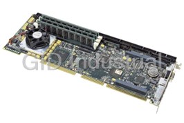


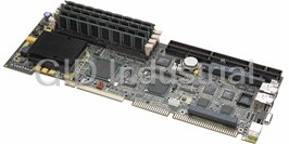
Request a Quote

The quote request has been received
Close

Facing challenges or have inquiries? Feel free to contact us!
Call Us +1-469-283-2440
What they say about us
FANTASTIC RESOURCE
One of our top priorities is maintaining our business with precision, and we are constantly looking for affiliates that can help us achieve our goal. With the aid of GID Industrial, our obsolete product management has never been more efficient. They have been a great resource to our company, and have quickly become a go-to supplier on our list!
Bucher Emhart Glass
EXCELLENT SERVICE
With our strict fundamentals and high expectations, we were surprised when we came across GID Industrial and their competitive pricing. When we approached them with our issue, they were incredibly confident in being able to provide us with a seamless solution at the best price for us. GID Industrial quickly understood our needs and provided us with excellent service, as well as fully tested product to ensure what we received would be the right fit for our company.
Fuji
HARD TO FIND A BETTER PROVIDER
Our company provides services to aid in the manufacture of technological products, such as semiconductors and flat panel displays, and often searching for distributors of obsolete product we require can waste time and money. Finding GID Industrial proved to be a great asset to our company, with cost effective solutions and superior knowledge on all of their materials, it’d be hard to find a better provider of obsolete or hard to find products.
Applied Materials
CONSISTENTLY DELIVERS QUALITY SOLUTIONS
Over the years, the equipment used in our company becomes discontinued, but they’re still of great use to us and our customers. Once these products are no longer available through the manufacturer, finding a reliable, quick supplier is a necessity, and luckily for us, GID Industrial has provided the most trustworthy, quality solutions to our obsolete component needs.
Nidec Vamco
TERRIFIC RESOURCE
This company has been a terrific help to us (I work for Trican Well Service) in sourcing the Micron Ram Memory we needed for our Siemens computers. Great service! And great pricing! I know when the product is shipping and when it will arrive, all the way through the ordering process.
Trican Well Service
GO TO SOURCE
When I can't find an obsolete part, I first call GID and they'll come up with my parts every time. Great customer service and follow up as well. Scott emails me from time to time to touch base and see if we're having trouble finding something.....which is often with our 25 yr old equipment.
ConAgra Foods