

 Manufacturers
GESPAC GESSBS-6A
Description
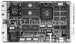
GESPAC GESSBS-6A CPU Board. 68000 Single Board System.
Part Number
GESSBS-6A
Price
Request Quote
Manufacturer
GESPAC
Lead Time
Request Quote
Category
PRODUCTS - G
Features
- 1 Mbytes of EPROM optional
- 16/32 bit architecture with 8/16 MHz 68000/68010 microprocessor
- 256 Kbytes of CMOS static RAM are protected against the power fail
- 512 Kbytes of SRAM and 256 Kbytes of EPROM or 256 Kbytes of SRAM and 512 Kbytes of EPROM
- 8 Mbytes of external memory addressing capability
- Fully compatible G-64 and G-96 Bus
- One channel supports asynchronous and synchronous protocols and provides all signals necessary for a modem
- Programmable baud rates from 0 to 38400 Bauds (async) and from 0 to 800 Kbits/s (sync)
- Real-Time-Clock Calendar with on-board battery backup
- Standard power supply : + 5 V (± 12 V optional)
- Three independent 16-bit counter/timers
- Two 8-bit double buffered bidirectional I/O ports with four handshake lines. These ports can be linked to form a single 16-bit I/O port
- Two independent RS 232-C full-duplex serial channels
- Two timers can be linked to form a 32-bit timer/counter
- Watch Dog circuit for program security
Datasheet

Extracted Text
GESSBS-6A PROCESSORS Third edition 68000 SINGLE BOARD SYSTEM The GESSBS-6A 68000 Single Board System offers unique features available for the first time on single Euroboard format. Built around the 68000 16/32 bit CPU running at 8 MHz or 16 MHz, the module has 256 Kbytes of zero wait-state CMOS static RAM. A power fail logic with the addition of an external battery, protect the integrity of the data stored in CMOS static Ram. Four 32-pin JEDEC sockets allow up to 512 Kbytes of EPROM or 256 Kbytes of EPROM plus 256 Kbytes of static RAM. 8 Mbytes of external memory can be addressed by the GESSBS-6A allowing system RAM extension. Two RS 232-C serial ports are available with an 8530 Serial Communications Controller chip. One channel supports asyn- chronous and synchronous protocols like monosync, IBM bisync, SDLC and HDLC. The second channel supports only asyn- chronous protocols. The GESSBS-6A includes two independent 8-bit bidirectional I/O ports and three independent 16-bit counter/timers (8536 CIO chip). A Real-Time-Clock Calendar (NS58274) with an on-board battery backup and Watch Dog circuit are implemented on the module. The GESSBS-6A is fully compatible with the standard G-64 and G-96 Bus. Technical features l16/32 bit architecture with 8/16 MHzlProgrammable baud rates from 0 to 38400 Bauds (async) 68000/68010 microprocessor and from 0 to 800 Kbits/s (sync) l512 Kbytes of SRAM and 256 Kbytes of EPROM orlTwo 8-bit double buffered bidirectional I/O ports 256 Kbytes of SRAM and 512 Kbytes of EPROM with four handshake lines. l1 Mbytes of EPROM optional These ports can be linked to form a single 16-bit I/O port l8 Mbytes of external memory addressing capabilitylThree independent 16-bit counter/timers l256 Kbytes of CMOS static RAM are protected againstlTwo timers can be linked to form a 32-bit the power fail timer/counter lReal-Time-Clock Calendar with on-board battery backuplWatch Dog circuit for program security lTwo independent RS 232-C full-duplex serial channelslFully compatible G-64 and G-96 Bus lOne channel supports asynchronous and synchronouslStandard power supply : + 5 V (± 12 V optional) protocols and provides all signals necessary for a modem Reference GESSBS-6A: 68000 Single Board System © GESPAC SA, 1994 XDD-GESSBS-6A GESSBS-6A . + 5 V BAT GND A1-A23 CHAIN OUT TXD RS-232-C DCE/DTE TXC Channel 1 Interface Selection PAGE 1 RXD Asynchronous PAGE 0 8530 SDCC RXC & RTS Serial A0-A23 Synchronous CTS Communication Communication DCD Controller VMA DSR RS-232-C DCE/DTE VPA DTR Interface Selection DS0 DS1 R/W GND +5V Bat. DTACK TXD BERR RXD Channel 2 RTS Asynchronous D0-D15 G-64/G96 CTS Communication Watch 16-Bit CPU 256 K Bytes of Power DCD Interface SYSCLK 68000/68010 CMOS Dog Fail DSR Logic ENABLE 8 Mhz/16 Mhz Static RAM DTR Logic Logic HALT RESET BRQ BGRT/BGRT RTC BGACK Control IACK/IACK Power Fail Logic D0-D15 & Battery A1-A23 NMI PWF IRQ1 IRQ2 PA0-PA7 IRQ3 8536 CIO 512 K Bytes of EPROM 58274 RTC IRQ4 PB0-PB7 3x16 bit timers Control or IRQ5 Real Time Clock & 256 K Bytes of EPROM Logic Calendar PC0-PC3 2x8 bit I/O Ports 256 K Bytes of SRAM Figure 1.1 Block Diagram GESSBS-6A . 1. GENERAL INFORMATION The GESSBS-6A is fully compatible with the standard G-64 and G-96 Bus. The block diagram of figure 1.1 illustrates the different parts of the module and their interconnections. 1.1 DESCRIPTION Using Surface Mounting Device and very high PCB techno- 1.2 SPECIFICATIONS logy, it has been possible to offer a complete 68000 system on a single Euroboard format. Microprocessors : 68000 The GESSBS-6A is built around the 68000 16/32 bit CPU CPU clock : 8 MHz or 16 MHz running at 8 MHz or 16 MHz and has 256 Kbytes of zero wait-state CMOS static RAM. A power fail logic with the Data transfer : 8/16-bit, syn/asynchronous addition of an on-board battery, protect the integrity of data Synchronous transfer : 1 MHz or 2 MHz Enable stored in the CMOS static RAM. Four 32-pin JEDEC sockets frequency clock allow up to 512 Kbytes of EPROM or 256 Kbytes of EPROM Timeout delay : 8 µs or 16 µs plus 256 Kbytes of static RAM. The EPROM can operate at Wait-states : SRAM : 0 or 1 zero wait-sate (120 ns EPROM time access). 8 Mbytes of external asynchronous memory can be addressed by the EPROM : 0, 1, 2 or 4 GESSBS-6A allowing important system RAM extension. Addressing capability : Two RS 232-C serial channels are available with an 8530 Internal memory : - 256 Kbytes of CMOS low SCC chip. One channel supports asynchronous and synchro- power SRAM nous protocols like monosync, IBM bisync, SDLC and - 512 Kbytes of EPROM HDLC. This channel provides all the signals necessary for or 256 Kbytes of EPROM plus modem connection. The second channel supports only 256 Kbytes of SRAM asynchronous protocols and allows terminal connection. The or 1 Mbyte of EPROM speed of transmission is independently programmable for each channels from 0 to 38400 Bauds for asynchronous External memory : 8 Mbytes protocols. External peripheral : 2 Kbytes ( 1 K x 16) The module includes two independant 8-bit, double-buffered bidirectional I/O ports plus a 4-bit special-purpose I/O port 8530 clock input : 3.6864 MHz (8536 CIO). The 8536 CIO features flexible pattern-recogni- Serial channel 1 : 8530 SCC channel A tion logic, four handshake modes (including 3-Wire like the Available protocols : Asynchronous, monosync, IEEE-488). The two 8-bit I/O ports can be linked to form a IBM bisync, SDLC and HDLC single 16-bit I/O port. Interface : RS 232-C compatible The 8536 CIO provides three independant 16-bit Signals for modem : Yes counter/timers with up to four external command/control lines per counter/timer (count input, output, gate and trigger) Progr. data rates : 0-38400 Bauds (async) and three output duty cycles (pulsed, one-shot and square 0-800 Kbits/s (sync) wave), programmable as retriggerable or nonretriggerable. Channel configuration : DCE or DTE Two 16-bit counter/timers can be linked to form a 32-bit counter/timer. Serial channel 2 : 8530 SCC channel B A Real-Time-Clock Calendar (NS58274), with an on-board Available protocols : Asynchronous battery backup indicates time and date and can generate a Interface : RS 232-C compatible programmable interrupt. Signals for modem : No The module implements a "Watch Dog" function which can Progr. data rates : 0-38400 Bauds (async) generate a reset or a level 7 interrupt. Channel configuration : DCE or DTE Five interrupt bus lines (level 1 - level 5) are selectable to be vectored or autovectored. All the internal interrupts are on Parallel communication : Two 8-bit bouble-buffered the level 6. Four interrupt sources can activate the level 7 : bidirectional ports plus a 4-bit NMI bus line, PWF bus line, ABORT external switch and special purpose I/O port Watch Dog Fail signal. A status register contains the source of level 7 interrupt. Progr. timer features : 3 independent 16-bit A control register permits selection of one of four possible timer/counters cascadable to memory maps. form a 32-bit timer/counter Interrupt capability for each Control lines for direct memory access operations (DMA) are timer accessible on the bus. Note that DMA operations can not be realized on the on-board local RAM. A timeout logic controls Timer clock origin : External or internal 2 MHz asynchronous operations when the transfer execution is not possible. GESSBS-6A . CPU BUS Physical RTC interrupt 0.1, 0.5, 1, 5, 10, 30 Byte address Word address Field size address time intervals : and 60 sec (hexadecimal) (hexadecimal) space RTC functions : Hours, minutes, seconds, day, 5 month, year FFFFFF Do not care 256 Kbytes Internals EPROM / Battery life time approx. : 15000 hours SRAM FC0000 U13, U14 Bus interface : - Address bus : 3 states TTL 5 compatible FBFFFF Do not care 256 Kbytes Internals EPROM - Data bus : 3 states TTL F80000 U15, U16 compatible - Other signals : TTL compatible F7FFFF Do not care 256 Kbytes Internal Low F40000 Power SRAM Bus drivers : 48 mA device type Power requirements : + 5 Vdc : 1.75 A typ* Not used Operating temperature : + 5° to + 55 C° 1 8207FF 4103FF 2 Kbytes Asynchronous PCB dimensions : 100 x 160 mm 2 820000 410000 External I/O * Without U13 / U14 / U15 / U16 devices Reserved Table 1.1 Specifications 3 81007F Do not care 64 Kbytes Internal I/O 810000 Reserved 1.3 MEMORY MAP 1 8007FF 4003FF 2 Kbytes Synchronous The GESSBS-6A module has been designed to work either 2 800000 400000 External I/O on the G-64 or on the G-96 Bus. With the G-64 Bus, the external memory which can be added to the module is 7FFFFF 3FFFFF 7680 External limited at 128 K x 16 (256 Kbytes). Nevertheless with the Kbytes Memory G-96 Bus, this limitation is fixed at 8 Mbytes allowing 080000 040000 G-96 only important system memory extension. 07FFFF 03FFFF 256 Kbytes External Addresses on the bus are considered as word addresses. Memory The upper and lower bytes are selected by DS0 and DS1 040000 020000 G-64 & G-96 bus lines. Therefore the address line A1 of the 68000 drives the A0 line on the bus. 4 03FFFF 01FFFF 256 Kbytes Mapping 3 : MAP1 = 1, The four possible memory maps generated by the MAP0 = 1 GESSBS-6A module are shown in table 1.2. External Memory 000000 000000 G-64 & G-96 4 03FFFF Do not care 256 Kbytes Mapping 2 : MAP1 = 1, MAP0 = 0 U13, U14 EPROM/ 000000 SRAM 4 03FFFF Do not care 256 Kbytes Mapping 1 : MAP1 = 0, 1 Notes: External field is characterized on the bus by the MAP0 = 1 Internal Low VPA signal and A0-A9 address line. 000000 Power SRAM 2 External I/O module allow access by word. If the I/O module is an 8-bit module, the high byte on D8- 4 03FFFF Do not care 256 Kbytes Mapping 0 : D15 bus lines is unused. MAP1 = 0, MAP0 = 0 3 Internal I/O are redundant, refer to § 1.3.1 Internal 4 After power on or restart operation, this area is EPROM/ relocated in the internal EPROM field (mapping 0). 000000 U15, U16 Refer to § 1.4. 5 1 Mbyte EPROM version refer to § 2.18. Table 1.2 Memory map GESSBS-6A . 1.3.1 INTERNAL I/O MAP 1.4 MAPPING CONTROL REGISTER The asynchronous address field allows the access of the After power on or restart operations, the area $000000 - internal peripheral devices: 8530 SCC, 8536 CIO, 58274 $03FFFF is redundant with the internal EPROM field loca- RTC and the control/status register. ted at the addresses $F80000 - $FBFFFF. The internal I/O field is redundant. Therefore, it is recom- The attribution of the address field $000000 - $03FFFF mended to use the addresses that are shown in table 1.3 for (256 Kbytes) is controlled by two bits (MAP1, MAP0) of the software compatibility and running. control register located at the address $810061 as shown in the figure 1.2. The table 1.4 shows how to select one of the four possible module mapping. CPU Physical address Access type DEVICES Reserved Address : $810061 (write only) $810071 Byte Level 7 interrupt D7 D6 D5 D4 D3 D2 D1 D0 control status register $810069 Byte Watchdog trigger * * * * * * MAP1 MAP0 register Reserved *Unused bits $810061 Byte Mapping control Figure 1.2 Mapping control register Register Reserved MAP1 MAP0 CPU Byte Redundant CPU Physical address $81005F Byte 58274 RTC address byte address space $810041 0 0 $03FFFF $FBFFFF Internal EPROM Reserved $000000 $F80000 U15, U16 $810027 Byte 8530 SCC 0 1 $03FFFF $F7FFFF Internal Low $810021 $000000 $F40000 Power SRAM Reserved 1 0 $03FFFF $FFFFFF Internal EPROM/ $000000 $FC0000 SRAM U13, U14 $810007 Byte 8536 CIO $810001 1 1 $03FFFF - - - External memory $000000 Table 1.3 Internal I/O map Notes: After power on or restart operations, MAP1 and MAP0 control bits are cleared Table 1.4 Mapping selection GESSBS-6A . 1.5 LEVEL 7 INTERRUPT CONTROL/STATUS 1.6 RESTART OPERATION REGISTER The RESET is an output signal generated by the GESSBS- 6A module during power on, the software instruction Four interrupt sources are wired on the interrupt level 7 of «RESET» or by depressing the external Reset-switch. the CPU : NMI bus line, PWF bus line, ABORT external switch signal and Watch Dog Fail signal. A Control/Status The reset circuitry is made with the TI 7702 device which register located at address $810071 allows to know the generates automatically a RESET signal during either the source of this interrupt and after to clear it as described in power-on sequence or when the power supply drops figure 1.3. under the nominal voltage of 4.75 V typ. Thus, it is very important to ensure a correct + 5 V power supply. Address : $810071 (read/write) D7 D6 D5 D4 D3 D2 D1 D0 1.7 8536 COUNTER/TIMER AND PARALLEL I/O UNIT PWF * * * * WDF NMI ABORT 1.7.1 GENERAL DESCRIPTION *Unused bits The 8536 CIO is a general-purpose peripheral circuit, satis- ABORT When set, this bit indicates that the external fying most counter/timer and parallel I/O needs encounte- ABORT switch has been depressed. While this red in system designs. This versatile device contains three bit is a one, a non-maskable interrupt (level 7) I/O ports and three counter/timers. is generated to the CPU The features of the 8536 CIO are listed below : SET ABORT external switch – Two independent 8-bit, double-buffered, bidirectional I/O depressed ports plus a 4-bit special-purpose I/O port. I/O ports CLEARED CPU writes a one feature programmable polarity, programmable direction NMI When set, this bit indicates that a Non- (Bit mode), «pulse catchers» and programmable open- Maskable Interrupt (NMI) request has occured drain output. on the G-64/G-96 Bus. While this bit is a one, a – Four handshake modes, including 3-Wire (like the IEEE- non-maskable interrupt (level 7) is generated to 488). the CPU. – Flexible pattern-recognition logic, programmable as a 16- vector interrupt controller. SET NMI bus line asserted low – Three independent 16-bit counter/timers with up to four CLEARED CPU writes a one external access lines per counter/timer. WDF When set, this bit indicates that the Watch Dog logic has generated an interrupt. While this bit is a one, a non-maskable interrupt (level 1.7.2 8536 REGISTERS 7) is generated to the CPU. The 8536 CIO contains 45 registers which are not directly SET Watch Dog Fail signal asserted accessible by the CPU. Only four registers are directly low accessible as shown in table 1.5. CLEARED CPU writes a one PWF Power Failure Detected. This bit reflects the Physical Address Access Register name condition of the PWF bus line. This state is the logical complement of this line. While this bit is $810001 R/W Port C's Data Register a one, a non-maskable interrupt (level 7) is $810003 R/W Port B's Data Register generated to the CPU. $810005 R/W Port A's Data Register SET The power supply is defective $810007 R/W Control Register CLEARED CPU writes a one and the power supply is correct Table 1.5 8536 CIO directly accessible register map Important notes : The internal registers are accessed by the folowing two- - All these interrupts sources are latched on their falling step sequence : edge. First, write the address of the target register into the - After power on or restart operation, before unmasking Control Register ; then read from or write to the target the interrupts, the interrupt control/status register must register by accessing the Control Register for the second be initialized with the pattern 1XXXX111 by the CPU. time. Note that the data registers can be accessed by the same way but it is most useful to make a direct access of Figure 1.3 Interrupt Control/Status register these registers. Table 1.6 gives the target addresses of the 8536 CIO's registers. GESSBS-6A . The figure 1.4 describes the contents of the 8536 CIO Target register Target register name registers. For more information regarding 8536 register address promming, please refer to the “Z8036/Z8536 CIO Counter/Timer and Parallel I/O Unit tecchnical manual” $00 Master Interrupt Control from Zilog. $01 Master Configuration Control $02 Port A's Interrupt Vector Master Interrupt Control Register Address : 000000 $03 Port B's Interrupt Vector (Read/Write) $04 Counter/Timer's Interrupt Vector $05 Port C's Data Path Polarity D D D D D D D D 7 6 5 4 3 2 1 0 $06 Port C's Data Direction MASTER INTERRUPT RESET ENABLE (MIE) $07 Port C's Special I/O Control RIGHT JUSTIFIED ADDRESSES DISABLE LOWER CHAIN (DLC) 0 = SHIFT LEFT (A from AD ) 0 1 $08 Port A's Command and Status 1 = RIGHT JUSTIFY (A0 from AD0) NO VECTOR (NV) $09 Port B's Command and Status COUNTER/TIMERS VECTOR PORT A VECTOR INCLUDES INCLUDES STATUS (CT VIS) $0A Counter/Timer 1's Command and Status STATUS (PA VIS) PORT B VECTOR INCLUDES $0B Counter/Timer 2's Command and Status STATUS (PB VIS) $0C Counter/Timer 3's Command and Status $0D Port A's Data* Master Configuration Control Register Address : 000001 $0E Port B's Data* (Read/Write) $0F Port C's Data* $10 Counter/Timer 1's Current Count-MSB D D D D D D D D 7 6 5 4 3 2 1 0 $11 Counter/Timer 1's Current Count-LSB PORT B COUNTER/TIMER LINK ENABLE (PBE) CONTROLS (LC) $12 Counter/Timer 2's Current Count-MSB COUNTER/TIMER 1 LC1 LC2 $13 Counter/Timer 2's Current Count-LSB ENABLE (CT1E) 0 0 COUNTER/TIMERS INDEPENDENT 0 1 C/T 1's OUTPUT GATES C/T 2 $14 Counter/Timer 3's Current Count-MSB COUNTER/TIMER 2 1 0 C/T 1's OUTPUT TRIGGERS C/T 2 ENABLE (CT2E) 1 1 C/T 1's OUTPUT IS C/T 2's $15 Counter/Timer 3's Current Count-LSB COUNT INPUT PORT C AND COUNTER/ $16 Counter/Timer 1's Time Constant MSB TIMER 3 ENABLE PORT A ENABLE (PAE) (PCE AND CT3E) PORT LINK CONTROL (PLC) $17 Counter/Timer 1's Time Constant LSB 0 = PORTS A AND B OPERATE INDEPENDENTLY 1 = PORTS A AND B ARE LINKED $18 Counter/Timer 2's Time Constant MSB $19 Counter/Timer 2's Time Constant LSB Port Mode Specification Registers $1A Counter/Timer 3's Time Constant MSB Address : 100000 Port A $1B Counter/Timer 3's Time Constant LSB 101000 Port B $1C Counter/Timer 1's Mode Specification (Read/Write) $1D Counter/Timer 2's Mode Specification D D D D D D D D 7 6 5 4 3 2 1 0 $1E Counter/Timer 3's Mode Specification PORT TYPE LATCH ON PATTERN MATCH (LPM) $1F Current Vector SELECTS (PTS) (BIT MODE) DESKEW TIMER ENABLE (DTE) PTS1 PTS0 $20 Port A's Mode Specification (HANDSHAKE MODES) 0 0 BIT PORT 0 1 INPUT PORT $21 Port A's Handshake Specification PATTERN MODE SPECIFICATION 1 0 OUTPUT PORT BITS (PMS) 1 1 BIDIRECTIONAL $22 Port A's Data Path Polarity PMS1 PMS0 PORT 0 0 DISABLE PATTERN MATCH $23 Port A's Data Direction INTERRUPT ON TWO 0 1 “AND” MODE BYTES (ITB) 1 0 “OR” MODE $24 Port A's Special I/O Control 1 1 “OR PRIORITY ENCODED SINGLE BUFFERED VECTOR” MODE $25 Port A's Pattern Polarity MODE (SB) INTERRUPT ON MATCH ONLY $26 Port A's Pattern Transition $27 Port A's Pattern Mask Port Handshake Specification Registers $28 Port B's Mode Specification Address : 100001 Port A $29 Port B's Handshake Specification 101001 Port B (Read/Write) $2A Port B's Data Path Polarity $2B Port B's Data Direction D D D D D D D D 7 6 5 4 3 2 1 0 $2C Port B's Special I/O Control HANDSHAKE SPECIFICATION DESKEW TIME SPECIFICATION BITS BITS (HTS) SPECIFIES THE MSB's OF DESKEW $2D Port B's Pattern Polarity HTS1 HTS0 TIMER TIME CONSTANT 0 0 INTERLOCKED HANDSHAKE LSB IS FORCET 1 $2E Port B's Pattern Transition 0 1 STROBED HANDSHAKE 1 0 PULSED HANDSHAKE $2F Port B's Pattern Mask 1 1 THREE-WIRE HANDSHAKE REQUEST/WAIT SPECIFICATION BIT (RWS) *Can be accessed directly RWS2 RWS1 RWS0 0 0 0 REQUEST/WAIT DISABLED 0 0 1 OUTPUT WAIT Table 1.6 8536 CIO indirectly accessible register map 0 1 1 INPUT WAIT 1 0 0 SPECIAL REQUEST 1 0 1 OUTPUT REQUEST 1 1 1 INPUT REQUEST GESSBS-6A . Port Command and Status Registers Port C Data Register Address : 001000 Port A Address : 001111 (this register can be accessed directly) 001001 Port B (Read/Write) (Read/Partial Write) D D D D D D D D 7 6 5 4 3 2 1 0 D D D D D D D D 7 6 5 4 3 2 1 0 INTERRUPT UNDER INTERRUPT ON ERROR (IOE) SERVICE (IUS) PATTERN MATCH FLAG (PMF) INTERRUPT ENABLE (IE) (READ ONLY) Pattern Polarity Registers (PP) INTERRUPT PENDING (IP) INPUT REGISTER FULL (IRF) Address : 100101 Port A (READ ONLY) IUS, IE, IP ARE WRITTEN USING D D D D D D D D 7 6 5 4 3 2 1 0 101101 Port B THE FOLLOWING CODE : OUTPUT REGISTER EMPTY (ORE) (READ ONLY) (Read/Write) 0 0 0 NULL CODE 0 0 1 CLEAR IP & IUS 0 1 0 SET IUS Pattern Transition Registers (PT) PM PT PP PATTERN SPECIFICATION 0 1 1 CLEAR IUS Address : 100110 Port A 0 0 X BIT MASKED OFF SET IP 1 0 0 D D D D D D D D 0 1 X ANY TRANSITION 7 6 5 4 3 2 1 0 101110 Port B CLEAR IP 1 0 1 1 0 0 ZERO SET IE 1 1 0 1 0 1 ONE (Read/Write) 1 1 0 ONE TO ZERO CLEAR IE 1 1 1 TRANSITION 1 1 1 ZERO TO ONE INTERRUPT ERROR (ERR) TRANSITION Pattern Mask Registers (PM) (READ ONLY) Address : 100111 Port A D D D D D D D D 7 6 5 4 3 2 1 0 101111 Port B Data Path Polarity Registers (Read/Write) Address : 100010 Port A 101010 Port B Counter/Timer Command and Status Registers 000101 Port C (4 LSBs only) Address : 001010 Counter/Timer 1 (Read/Write) 001011 Counter/Timer 2 D D D D D D D D 7 6 5 4 3 2 1 0 001100 Counter/Timer 3 (Read/Partial Write) DATA PATH POLARITY (DPP) 0 = NON-INVERTING D D D D D D D D 1 = INVERTING 7 6 5 4 3 2 1 0 INTERRUPT UNDER COUNT IN PROGRESS (CIP) SERVICE (IUS) (READ ONLY) Data Direction Registers INTERRUPT ENABLE (IE) TRIGGER COMMAND BIT (TCB) Address : 100011 Port A (WRITE ONLY - READ RETURNS 0) 101011 Port B INTERRUPT PENDING (IP) GATE COMMAND BIT (GCB) 000110 Port C (4 LSBs only) IUS, IE, IP ARE WRITTEN USING THE FOLLOWING CODE : READ COUNTER CONTROL (RCC) (Read/Write) (READ/SET ONLY – 0 0 0 CLEARED BY READING CCR LSB) NULL CODE D D D D D D D D 7 6 5 4 3 2 1 0 0 0 1 CLEAR IP & IUS 0 1 0 SET IUS DATA DIRECTION (DD) 0 1 1 CLEAR IUS 0 = OUTPUT BIT 1 0 0 1 = INPUT BIT SET IP CLEAR IP 1 0 1 1 1 0 SET IE Special I/O Control Registers 1 1 1 CLEAR IE Address : 100100 Port A INTERRUPT ERROR (ERR) (READ ONLY) 101100 Port B 000111 Port C (4 LSBs only) (Read/Write) Counter/Timer Mode Specification Registers Address : 011100 Counter/Timer 1 D D D D D D D D 7 6 5 4 3 2 1 0 011101 Counter/Timer 2 SPECIAL INPOUT/OUTPUT (SIO) 011110 Counter/Timer 3 0 = NORMAL INPUT OR OUTPUT 1 = OUTPUT WITH OPEN DRAIN OR (Read/Write) INPUT WITH 1's CATCHER D D D D D D D D 7 6 5 4 3 2 1 0 Port Data Registers CONTINUOUS SINGLE OUTPUT DUTY CYCLE CYCLE (C/CS) SELECTS (DCS) Address : 001101 Port A (this register can be accessed directly) EXTERNAL OUTPUT DCS1 DCS2 001110 Port B (this register can be accessed directly) ENABLE (EOE) 0 0 PULSE OUTPUT (Read/Write) 0 1 ONE-SHOT OUTPUT EXTERNAL COUNT 1 0 SUQARE-WAVE OUTPUT ENABLE (ECE) 1 1 DO NOT SPECIFY D D D D D D D D 7 6 5 4 3 2 1 0 EXTERNAL TIGGER RETRIGGER ENABLE BIT (REB) ENABLE (ETE) EXTERNAL GATE ENABLE (EGE) GESSBS-6A . Counter/Timer Current Count Registers 1.7.3 8536 INTERRUPTS Address : 010000 Counter/Timer 1's MSB 010001 Counter/Timer 1's LSB The 8536 CIO can generate a vectored interrupt when one 010010 Counter/Timer 2's MSB of the following conditions has occured : 010011 Counter/Timer 2's LSB a) A pattern match occuring in a bit port 010100 Counter/Timer 3's MSB 010101 Counter/Timer 3's LSB b) Another byte becoming available in an input port with (Read Only) handshake D D D D D D D D D D D D D D D D 7 6 5 4 3 2 1 0 7 6 5 4 3 2 1 0 c) A counter/timer reaching its terminal count MOST LEAST SIGNIFICANT SIGNIFICANT Five potential sources of interrupts are available. The priori- BYTE BYTE ties of these sources are fixed in the following order (highest to lowest) : Counter/Timer Constant Registers Address : 010110 Counter/Timer 1's MSB 1) Counter/Timer 3 HIGHEST 010111 Counter/Timer 1's LSB 2) Port A 011000 Counter/Timer 2's MSB 011001 Counter/Timer 2's LSB 3) Counter/Timer 2 011010 Counter/Timer 3's MSB 4) Port B 011011 Counter/Timer 3's LSB (Read/Write) 5) Counter/Timer 1 LOWEST D D D D D D D D D D D D D D D D 7 6 5 4 3 2 1 0 7 6 5 4 3 2 1 0 All internal interrupts of the GESSBS-6A are on the level 6. MOST LEAST The CIO interrupt priority, relative to other components SIGNIFICANT SIGNIFICANT BYTE BYTE (8530 SCC and 58274 RTC), is fixed as described below : 1) 8536 CIO HIGHEST Interrupt Vector Registers Address : 000010 Port A 2) 8530 SCC 000011 Port B 3) 58274 RTC LOWEST 000100 Counter/Timers (Read/Write) WARNING : The 8536 needs a recovery time of 650 ns D D D D D D D D 7 6 5 4 3 2 1 0 min. between each access. With a 16 MHz CPU, this value is not respected when using instructions like BTST and INTERRUPT VECTOR PORT VECTOR STATUS BCLR. PRIORITY ENCODED VECTOR MODE : D D D 3 2 1 x x x NUMBER OF HOGHEST PRIORITY BIT WITH A MATCH 1.8 8530 SERIAL COMMUNICATIONS ALL OTHER MODES : D3 D2 D1 ORE IRF PMF NORMAL CONTROLLER 0 0 0 ERROR COUNTER/TIMER STATUS : D D 2 1 1.8.1 GENERAL DESCRIPTION 0 0 C/T 3 0 1 C/T 2 1 0 C/T 1 1 1 ERROR The 8530 SCC Serial Communication Controller is designed for multifunction support for handling the large variety of Current Vector Register serial communication protocols available. The 8530 can be Address : 011111 programmed to satisfy special serial communications requi- (Read only) rements as well as to follow standard formats such as byte- oriented synchronous and asynchronous. D D D D D D D D 7 6 5 4 3 2 1 0 INTERRUPT VECTOR BASED The features of the 8530 SCC are listed below : ON HIGHEST PRIORITY UNMASKED IP. IF NO INTERRUPT PENDINGlTwo independent full-duplex channels, ALL 1's OUTPUT. Receiver data registers quadruply buffered, Transmitter data registers double buffered, Notes :Write a "1" will select the register bit's function. Baud rate generator in each channel, Write a "0" will deselect the register bit's function. Digital Phase-Locked Loop for clock recovery, Figure 1.4 8536 CIO registers NRZ, NRZI, and FM encoding/decoding. GESSBS-6A . lAsynchronous capabilities : The table 1.8 gives the target addresses of the 8530 SCC's 5, 6, 7 or 8 bits per character, registers. 1 1, 1 / or 2 stop bits, 2 Odd or even parity, Times 1, 16, 32 or 64 clock modes, Target Name Access Target register functions Break generation and detection, register Parity, overrun and framing error detection. Address lByte-oriented synchronous capabilities : $0 WR0 Write CRC initialize, registers pointers* Internal character synchronization, $0 RR0 Read Transmit/receive buffer and 1 or 2 sync characters in separate registers, external status* Automatic sync character insertion and deletion, Cyclic redundancy check (CRC) generation/detection, $1 WR1 Write Transmit/receive interrupt mode 6 or 8-bit sync character. $1 RR1 Read Special receive condition status lSDLC / HDLC capabilities : $2 WR2 Write Interrupt vector Abort sequence generation and checking, $2 RR2 Read Interrupt vector Automatic zero insertion and deletion, $3 WR3 Write Receive parameters and controls Automatic flag insertion between messages, Address field recognition, $3 RR3 Read Interrupt pending bits I-field residue handling, $4 WR4 Write Transmit/receive miscellaneous CRC generation/deletion, parameters/modes SDLC loop mode with EOP recognition, $5 WR5 Write Transmit parameters and loop entry and exit. controls $6 WR6 Write Sync character or SSDLC address field 1.8.2 8530 REGISTERS $7 WR7 Write Sync character or SDLC flag The 8530 SCC contains 13 registers in each channel that $8 WR8 Write Transmit buffer* allow the configuration of the functional characteristic of $8 RR8 Read Receive buffer* the channels. Only six registers are directly accessible by $9 WR9 Write Master interrupt control the CPU, as shown in table 1.7, allowing access to the and reset other 8530 registers. $A WR10 Write Miscellaneous transmitter/ reveiver control bits Physical Address Access Register name $A RR10 Read Miscellaneous status $B WR11 Write Clock mode control $810021 W Channel B Control Register $C WR12 Write Lower byte of baud rate $810021 R Channel B Status Register generator time constant $810023 R/W Channel B Data Register $C RR12 Read Lower byte of baud rate $810025 W Channel A Control Register generator time constant $810025 R Channel A Status Register $D WR13 Write Upper byte of baud rate $810027 R/W Channel A Data Register generator time constant $D RR13 Read Upper byte of baud rate Table 1.7 8530 SCC directly accessible register map generator time constant $E WR14 Write Miscellaneous control bits Notes : $F WR15 Write External/status interrupt control The Control Register is the WRO 8530 register The Status Register is the RRO 8530 register $F RR15 Read External/status interrupt The Data Register, in write access, is the WR8 8530 register information The Data Register, in read access, is the RR8 8530 register The 8530 SCC uses the same two-step sequence as the 8536 * Can be accessed directly CIO, to access the internal registers. First, write the address of Table 1.8 8530 SCC indirectly accessible register map. the target register into the Control Register of the concerned channel; then read or write to the target register by accessing The figure 1.5 describes the contents of the 8530 SCC regis- the Control Register for the second time. Note that the Data ters. For more information regarding 8530 registers program- registers can be accessed in the same way but it is most ming, please refer to “Z8030/Z8530 SCC Serial useful to make a direct access of these registers. Communication Controller technical manual” from Zilog. GESSBS-6A . Read Register 0 Read Register 12 D D D D D D D D D D D D D D D D 7 6 5 4 3 2 1 0 7 6 5 4 3 2 1 0 Rx CHARACTER AVAILABLE TC 0 ZERO COUNT TC 1 Tx BUFFER EMPTY TC 2 DCD TC 3 LOWER BYTE OF TIME CONSTANT SIYNC/HUNT TC 4 CTS TC 5 Tx UNDERRUN/EOM TC 6 BREAK/ABORT TC 7 Read Register 1 Read Register 13 D D D D D D D D D D D D D D D D 7 6 5 4 3 2 1 0 7 6 5 4 3 2 1 0 ALL SENT TC 8 RESIDUE CODE 2 TC 9 RESIDUE CODE 1 TC 10 RESIDUE CODE 0 TC 11 UPPER BYTE OF TIME CONSTANT PARITY ERROR TC 12 Rx OVERRUN ERROR TC 13 CRC/FRAMING ERROR TC 14 END OF FRAME (SDLC) TC 15 Read Register 2 Read Register 15 D D D D D D D D D D D D D D D D 7 6 5 4 3 2 1 0 7 6 5 4 3 2 1 0 V 0 0 V ZERO COUNT IE 1 V 0 2 V DCD IE 3 INTERRUPT VECTOR* V SYNC/HUNT IE 4 V CTS IE 5 V Tx UNDERRUN/EOM IE 6 V BREAK/ABORT IE 7 * MODIFIED IN B CHANNEL Write Register 0 Read Register 3 D D D D D D D D 7 6 5 4 3 2 1 0 D D D D D D D D 7 6 5 4 3 2 1 0 0 0 0 REGISTER 0 CHANNEL B EXT/STAT IP* REGISTER 1 0 0 1 0 1 0 REGISTER 2 CHANNEL B Tx IP* 0 1 1 REGISTER 3 CHANNEL B Rx IP* 1 0 0 REGISTER 4 CHANNEL A EXT/STAT IP* 1 0 1 REGISTER 5 1 1 0 REGISTER 6 CHANNEL A Tx IP* 1 1 1 REGISTER 7 CHANNEL A Rx IP* 0 0 0 REGISTER 8 0 0 1 REGISTER 9 0 0 1 0 REGISTER 10 0 0 1 1 REGISTER 11 * 1 0 0 REGISTER 12 * ALWAYS 0 IN B CHANNEL 1 0 1 REGISTER 13 1 1 0 REGISTER 14 Read Register 10 1 1 1 REGISTER 15 0 0 0 NULL CODE D D D D D D D D 7 6 5 4 3 2 1 0 0 0 1 POINT HIGH 0 1 0 RESET EXT/STAT INTERRUPTS 0 0 1 1 SEND ABORT (SDLC) ON LOOP 1 0 0 ENABLE INT ON NEXT Rx CHARACTER 0 1 0 1 RESET TxINT PENDING ERROR RESET 1 1 0 0 1 1 1 RESET HIGHEST IUS LOOP SENDING 0 0 NULL CODE 0 0 1 RESET Rx CRC CHECKER RESET Tx CRC GENERATOR 1 0 TWO CLOCK MISSING 1 1 RESET Tx UNDERRUN/EOM LATCH ONE CLOCK MISSING * WITH POINT HIGH COMMAND GESSBS-6A . Write Register 1 Write Register 6 D D D D D D D D D D D D D D D D 7 6 5 4 3 2 1 0 7 6 5 4 3 2 1 0 EXT INT ENABLE Tx INT ENABLE PARITY IS SPECIAL CONDITION Rx INT DESABLE 0 0 SYNC SYNC SYNC SYNC SYNC SYNC SYNC SYNC MONOSYNC, 8 BITS 7 6 5 4 3 2 1 0 0 1 Rx INT ON FIRST CHARACTER OR SPECIAL CONDITIONS SYNC SYNC SYNC SYNC SYNC SYNC SYNC SYNC MONOSYNC, 6 BITS 1 0 5 4 3 2 1 0 1 0 INT ON ALL Rx CHARACTERS OR SPECIAL CONDITION SYNC SYNC SYNC SYNC SYNC SYNC SYNC SYNC BISYNC, 16 BITS 7 6 5 4 3 2 1 0 SYNC SYNC SYNC SYNC 1 1 1 1 BISYNC, 12 BITS Rx INT ON SPECIAL CONDITION ONLY 3 2 1 0 1 1 ADR ADR ADR ADR ADR ADR ADR ADR SDLC 7 6 5 4 3 2 1 0 ADR ADR ADR ADR x x x x SDLC 7 6 5 4 WAIT/DMA REQUEST ON RECEIVE/TRANSMIT (ADDRESS RANGE) WAIT/DMA REQUEST FUNCTION Write Register 7 WAIT/DMA REQUEST ENABLE D D D D D D D D 7 6 5 4 3 2 1 0 Write Register 2 D D D D D D D D 7 6 5 4 3 2 1 0 V 0 V 1 SYNC SYNC SYNC SYNC SYNC SYNC SYNC SYNC MONOSYNC, 8 BITS 7 6 5 4 3 2 1 0 SYNC SYNC SYNC SYNC SYNC SYNC x x MONOSYNC, 6 BITS V 5 4 3 2 1 0 2 SYNC SYNC SYNC SYNC SYNC SYNC SYNC SYNC BISYNC, 16 BITS 15 14 13 12 11 10 9 8 SYNC SYNC SYNC SYNC SYNC SYNC SYNC SYNC BISYNC, 12 BITS V 11 10 9 8 7 6 5 4 3 INTERRUPT 0 1 1 1 1 1 1 0 SDLC VECTOR V 4 V 5 Write Register 9 V 6 D D D D D D D D 7 6 5 4 3 2 1 0 V 7 VIS NV Write Register 3 DLC D D D D D D D D 7 6 5 4 3 2 1 0 MIE Rx ENABLE STATUS HIGH/STATUS LOW SYNC CHARACTER LOAD INHIBIT 0 ADDRESS SEARCH MODE (SDLC) 0 0 NO RESET Rx CRC ENABLE 0 1 CHANNEL RESET B CHANNEL RESET A 1 0 ENTER HUNT MODE 1 1 FORCE HARDWARE RESET AUTO ENABLES 0 0 Rx 5 BITS/CHARACTER Write Register 10 0 1 Rx 7 BITS/CHARACTER D D D D D D D D 1 0 Rx 6 BITS/CHARACTER 7 6 5 4 3 2 1 0 1 1 Rx 8 BITS/CHARACTER 6 BIT/8 BIT SYNC LOOP MODE D D D D D D D D Write Register 4 7 6 5 4 3 2 1 0 ABORT/FLAG ON UNDERRUN PARITY ENABLE MARK/FLAG IDLE PARITY EVEN/ODD GO ACTIVE ON POLL 0 0 SYNC MODE ENABLE 0 0 NRZ 0 1 1 STOP BIT/CHARACTER 0 1 NRZI 1 1 0 1 /2 STOP BIT/CHARACTER 1 0 FM1 (TRANSITION = 12) 1 1 2 STOP BIT/CHARACTER FM0 (TRANSITION = 0) 1 1 0 0 8 BIT SYNC CHARACTER CRC PRESET I/O 16 BIT SYNC CHARACTER 0 1 1 0 SDLC MODE (01111110 FLAG) Write Register 11 1 1 EXTERNAL SYNC MODE D D D D D D D D X1 CLOCK MODE 7 6 5 4 3 2 1 0 0 0 0 1 X16 CLOCK MODE 1 0 X32 CLOCK MODE 0 0 TRxC OUT = XTAL OUTPUT X64 CLOCK MODE 1 1 0 1 TRxC OUT = TRANSMIT CLOCK TRxC OUT = BR GENERATOR OUTPUT 1 0 D D D D D D D D 7 6 5 4 3 2 1 0 1 1 TRxC OUT = DPLL OUTPUT Write Register 5 TRxC I/O Tx CRC ENABLE RTS 0 0 TRANSMIT CLOCK = RTxC PIN 0 1 TRANSMIT CLOCK = TRxC PIN SDLC/CRC-16 TRANSMIT CLOCK = BR GENERATOR OUTPUT 1 0 Tx ENABLE 1 1 TRANSMIT CLOCK = DPLL OUTPUT SEND BREAK 0 0 RECEIVE CLOCK = RTxC PIN 0 0 Tx 5 BITS/CHARACTER RECEIVE CLOCK = TRxC PIN 0 1 Tx 7 BITS/CHARACTER 0 1 1 0 RECEIVE CLOCK = BR GENERATOR OUTPUT 1 0 Tx 6 BITS/CHARACTER 1 1 RECEIVE CLOCK = DPLL OUTPUT 1 1 Tx 8 BITS/CHARACTER RTxC XTAL/NO XTAL DTR GESSBS-6A . Write Register 12 c) Channel A external/status conditions D D D D D D D D 7 6 5 4 3 2 1 0 d) Channel B transmitter empty e) Channel B receiver full TC 0 TC f) Channel B external/status conditions 1 TC 2 Channel A interrupts are higher-priority than Channel B in- TC 3 LOWER BYTE OF terrupts, with the receiver, transmitter and external/status TIME CONSTANT TC 4 interrupts prioritized in that order within each channel. TC 5 All internal interrupts of the GESSBS-6A are on the level 6. TC 6 The SCC interrupt priority, relative to other components TC 7 (8536 CIO and 58274 RTC), is fixed as described below : Write Register 13 1) 8536 CIO HIGHEST 2) 8530 SCC D D D D D D D D 7 6 5 4 3 2 1 0 3) 58274 RTC LOWEST TC 8 TC 9 WARNING : TC 10 TC 1) In the 8530's interrupt routine, after the interrupt source 11 UPPER BYTE OF TIME CONSTANT has been cleared, a delay of 3 µs must be inserted prior TC 12 to exit from this routine. TC 13 2) The 8530 needs a recovery time of 1,8 µs min. between TC 14 each access. With a 16 MHz CPU, this value is not TC 15 respected when the 8530 is consecutively accessed. It is recommended to insert NOP instructions to reach this Write Register 14 specified delay. D D D D D D D D 7 6 5 4 3 2 1 0 BR GENERATOR ENABLE BR GENERATOR SOURCE 1.9 58274 REAL TIME CLOCK CALENDAR DTR/REQUEST FUNCTION AUTO ECHO 1.9.1 58274 REGISTERS LOCAL LOOPBACK 0 0 0 NULL COMMAND The 58274 chip adds to the GESSBS-6A board a real-time 0 0 1 ENTER SEARCH MODE clock and calendar function. A battery will maintain timekee- 0 1 0 RESET MISSING CLOCK 0 1 1 DISABLE DPLL ping, when the power supply is turned off. The register map 1 0 0 SET SOURCE = BR GENERATOR is shown in table 1.9. 1 0 1 SET SOURCE = RTxC 1 1 0 SET FM MODE 1 1 1 SET NRZI MODE Physical Address Access Register name $810041 R Status register Write Register 15 $810041 W Control register D D D D D D D D 7 6 5 4 3 2 1 0 $810043 R Tenths of seconds 0 $810045 R/W Unit seconds ZERO COUNT IE $810047 R/W Tens seconds 0 DCD IE $810049 R/W Units minutes SYNC/HUNT IE $81004B R/W Tens minutes CTS IE $81004D R/W Unit hours Tx UNDERRUN/EOM IE $81004F R/W Tens hours BREAK/ABORT IE $810051 R/W Unit days Notes :Write a "1" will select the register bit's function. $810053 R/W Tens days Write a "0" will deselect the register bit's function. $810055 R/W Unit months Figure 1.5 8530 CIO registers $810057 R/W Tens months $810059 R/W Unit years $81005B R/W Tens years 1.8.3 8530 INTERRUPTS $81005D R/W Day of week The 8530 SCC can generate a vectored interrupt when one $81005F R/W Clock setting/Interrupt registers of the following condition has occured : a) Channel A transmitter empty Table 1.9 RTC 58274 register map b) Channel A receiver full GESSBS-6A . The organisation of the registers is shown in the figures RS Register Select. The register select bit deter- 1.7 through 1.8. mines which of the two registers mapped onto For more information on the device, refer to the manufac- address 81005F will be accessed when this turer's data sheet. address is selected. a) Status Register (read only) RS Register selected Address : 810041 (Hexadecimal) 0 Clock setting register 1 Interrupt register 7 6 5 4 3 2 1 0 * * * * DCF 0 0 IF ISS Interrupt Start/Stop. The interrupt start/stop bit controls the running of the interrupt timer. It is programmed in the same way as the clock *Unused bits start/stop bit, a one to halt the interrupt and reset the timer, a zero to start interrupt timing. DCF Data-Changed Flag. This flag is set by the clock SET MPU writes a one setting pulse which also clocks the time regis- CLEARED MPU writes a zero ters. Testing this bit can tell the processor whether or not the time has change during a Figure 1.7 Status/Control Register read operation SET The time data has changed while a) Clock Setting Register (RS bit = 0)) being read out of the clock by the processor CLEARED Status register read Address : 81005F (Hexadecimal) IF Interrupt Flag. When this bit is one, it indicates 7 6 5 4 3 2 1 0 that an interrupt is pending. SET The interrupt timer times out * * * * LY1 LY0 AM/PM 12/24 CLEARED Status register read b) Control Register (write only) *Unused bits LY1-LY0 The leap year counter is a 2-stage binary coun- Address : 810041 (Hexadecimal) ter which should be loaded with the number of years since the last leap year. 7 6 5 4 3 2 1 0 AM/PM AM/PM indicator. The AM/PM indicator returns * * * * TST CSS RS ISS a zero for AM and a one for PM in the 12-hour mode. This bit is forced to zero in 24-hour mode. *Unused bits AM/PM indicator TST Test. A one written into the test bit puts the device into test mode. This allows setting of 0 AM the oscillator frequency. For normal operation the test bit is loaded with zero 1 PM CSS Clock Sart/Stop. A one stops the timekeeping of the clock and resets to zero the tenths of 12/24 12/24-hour mode. The 12/24-hour mode bit seconds counter. Timing is restarted when the determines whether the hours counter counts start/stop bit is written with a zero. from 1 to 12 or from 0 to 23. 12/24-hour bit 0 12-hour mode 1 24-hour mode SET MPU writes a one CLEARED MPU writes a zero GESSBS-6A . b) Interrupt Control Register (RS bit = 1) 1.9.2 58274 INTERRUPTS The interrupt generated by the 58274 RTC are wired on the Address : 81005F (Hexadecimal) level 6 of the CPU. These interrupts are autovectored. 7 6 5 4 3 2 1 0 The RTC interrupt priority, relative to other components (8536 CIO and 8530 SCC), is fixed as described below : * * * * S/R LP2 LP1 LP0 1) 8536 CIO HIGHEST 2) 8530 SCC 3) 58274 RTC LOWEST *Unused bits SR This bit determines the interrupt mode. 1.10 COMPLEMENTARY INFORMATION SR Mode For complementary information about the programming 0 Single interrupt procedure of the devices used on the GESSBS-6A, please refer to the manufacturer's data sheet. 1 Repeated interrupt - 8536 CIO “Z8536 Counter/Timer and Parallel I/O Unit technical manual” from ZILOG. LP2-LP0 These bits determine the time delay period that will occur between interrupts. - 8530 SCC “Z8530 Serial Communications Controller technical manual” from ZILOG. LP2 LP1 LP0 Time Delay - 58274 RTC “MM58274 Microprocessor Compatible Real Time Clock” from NATIONAL 0 0 0 No interrupt 0 0 1 0.1 second 0 1 0 0.5 second 0 1 1 1 second 1 0 0 5 seconds 1 0 1 10 seconds 1 1 0 30 seconds 1 1 1 60 seconds Figure 1.8 Clock Setting/Interrupt Control Register GESSBS-6A . 2. PREPARATION FOR USE, Designation Function INTERCONNECTIONS P1 G-64/G-96 Bus interface connector P2 External Reset and Abort switch connector 2.1 CONNECTOR AND JUMPERS P3 Parallel I/O and Timers connector IDENTIFICATION P4 Serial channel B connector P5 Serial channel A connector Table 2.1 identifies the jumpers and connectors of the GESSBS-6A module. Figure 2.1 shows their locations on J1 Watch Dog Fail Off/Reset/Interrupt selector the printed circuit. J2 Serial Channel B DCE/DTE configuration selector J3 Serial channel A Transmit/Receive clock selector J4 Serial channel A DCE/DTE configuration selector J5 – EPROM wait-states selector – U13/U14 EPROM/RAM selector J6 SRAM wait-states selector J7 U13/U14 devices selector J8 U13/U14 devices selector J9 U15/U16 EPROM type selector J10 – 8/16 MHz running frequency selector J11 – 8/16 µs bus timeout selector – Autovectored/vectored interrupt mode selector – 1/2 MHz Enable clock selector – 8/16 MHz running frequency selector – IACK/IACK signal selector – BGRT/BGRT signal selector J12 8/16 MHz CPU clock selector J13 U13/U14/U15/U16 devices selector J14 PWF Power Fail signal selector J15 SRAM battery backup selector J16 Enable-bus signal 3-state control J17 Bus system clock selector J18 U13/U14 devices selector J19 PG1 page extension selector J20 RTC battery backup on/off J23 2M x 1 bit EPROM selection LED – Red : SUPERVISOR mode – Green : Halt or Reset state Figure 2.1 Implementation – Yellow : External access Table 2.1 Connector, switch and jumper identification GESSBS-6A . 2.2 RESTART OPERATION Pin No Signal name Signal description Power-on reset is automatically generated on the module. External switches for reset and abort can be connected to 1 Protective Normally connected to P2 connector as illustrated on figure 2.2. Ground chassis The external reset switch reinitializes the GESSBS-6A 2 Transmit Data Direction : TO modem (DCE). module and activates the RESET signal on the G-64/G-96 (TxD) This line transfers data from a Bus. terminal to a modem. 3 Receive Data Direction : FROM modem. (RxD) This line transfers data from a 1 Reset Abort modem to a terminal. 2 Ground o o o 4 Request to Direction : TO modem Reset 3 Abort - NC Send (RTS) When active (high level), this o o o signal requires a data transfer 4 Abort - NO on TxD from the terminal to P2 o o o o o 5 + 5 Vdc the modem. 1 2 3 4 5 5 Clear to Send Direction : FROM modem. (CTS) When active (high level), this P2 pin assignment P2 external connection signal indicates that the Figure 2.2 External Reset/Abort switch connection modem is ready to receive a data transfer on TxD. CTS is the modem answer to RTS. 2.3 SERIAL COMMUNICATION INTERFACE 6 Data Set Ready Direction : FROM modem. (DSR) When active (high level), this signal indicates that the modem is connected and ready 2.3.1 GENERAL INFORMATION to receive terminal commands. The GESSBS-6A provides two RS 232-C serial interfaces 7 Signal Ground Signal is used as the reference driven by the 8530 SCC device (GND) potential. The first serial interface corresponding to channel A of the 8 Data Carrier Direction : FROM modem. 8530, allows asynchronous and synchronous communica- Detect (DCD) When active (high level), this tions and provides signals for modem connection. signal indicates that the modem is receiving a The second serial interface corresponding to channel B of telephone modulation within the 8530, allows only asynchronous communications. This the appropriate modem limits. interface is partial, but it is sufficient for terminal, mouse, etc. 9-14 Not used Interconnections on J4, J2 permit the configuring of the 15 TxC Direction : TO modem. interface of channels A and B respectively for DCE (Data Terminal clock output Communication Equipment) or DTE (Data Terminal 16 Not used Equipment) mode. 17 RxC Direction : FROM modem. The GESSBS-6A uses the GESPAC standard 3M 10-pin RS Terminal clock input 232-C connector (P4, P5) for each channel. Standard signals for the RS 232-C are defined in the table 2.2 and 18-19 Not used the pin assignment of P4/P5 connectors is shown in tables 20 Data terminal Direction : TO modem. 2.3 and 2.4. Ready (DTR) When active (high level), this Note : signal indicates to the The theorical speed limitation of the RS 232-C interface is modem that the terminal is 19200 Bauds with a cable of 15 meters. connected and operational. 21-25 Not used Notes :In RS 232-C (V24) sinal names are always specified in conjunction with the DTE DCE = Data Communication Equipment DTE = Data Terminal Equipment Table 2.2 RS 232-C 25-pin delta connector Light indicator GESSBS-6A . CTSB RTSB RxDB TxDB To channel B 3M 10-pin 3M 20-pin 25-pin delta P5 pin # RS 232-C pin # RS 232-C pin # RS 232-C o o o o o o (flat cable) (flat cable) (flat cable) signal 12 11 10 9 8 7 J2 1 2 3 4 5 6 1 1 1 GND o o o o o o 3 3 2 TxD 5 5 3 RxD 7 7 4 RTS DTR DSR + 12 V DCD CTS RTS RxD TxD To P4 9 9 5 CTS Figure 2.4 J2 pin assignment 2 11 6 DSR* 4 4 15 TxC J4 J2 6 14 20 DTR* 8 15 8 DCD* 14 13 12 11 10 9 8 12 11 10 9 8 7 10 8 17 RxC* o o o o o o o o o o o o o Table 2.3 Channel A (P5) connector pin assignment o o o o o o o o o o o o o 1 2 3 4 5 6 7 1 2 3 4 5 6 3M 10-pin 3M 20-pin 25-pin delta P4 pin # RS 232-C pin # RS 232-C pin # RS 232-C Figure 2.5 DCE configuration (flat cable) (flat cable) (flat cable) signal J4 J2 1 1 1 GND 3 3 2 TxD 14 13 12 11 10 9 8 12 11 10 9 8 7 5 5 3 RxD o o o o o o o o o o o o o 7 7 4 RTS 9 9 5 CTS o o o o o o o o o o o o o 2 11 6 DSR* 1 2 3 4 5 6 7 1 2 3 4 5 6 4 4 15 – 6 14 20 DTR* Figure 2.6 DTE configuration 8 15 8 DCD* 10 8 17 – 2.3.3 Tx and Rx CLOCK SELECTION * Important note : these RS 232-C signals can not be directly connected to a 3M 20-pin RS 232 connector or to a The transmit and receive clock for channel A can be selec- 25-pin delta RS 232 connector. If these signals are used, a ted to be either internal or external (synchronous opera- Null-Modem box must be inserted between the GES- tions) of the GESSBS-6A. When internal, the clock are SBS-6A and the transmitter/receiver module connected provide by the one-chip baud rate generator (inside the Table 2.4 Channel B (P4) connector pin assignment 8530 device). The clock selection for the channel A is shown in figure 2.7. To/from channel A RxCA TxCA 2.3.2 DCE/DTE CONFIGURATION 8 7 6 5 Signals defined in table 2.2 are connected to P4/P5 connectors respectively through the interconnection of o o o o J4/J2 as illustrated in fugures 2.3 and 2.4. J3 o o o o The figures 2.5 and 2.6 show the configuration of J4/J2 for two standard applications. For special configurations, refer to table 2.2 for signal definition and figure 2.3 and 2.4 for 1 2 3 4 their interconnections. To channel A DTRA DCDA CTSA RTSA RxDA TxDA To/from P5 RxC TxC o o o o o o o Figure 2.7 Tx and Rx clock selection for the Channel A 14 13 12 11 10 9 8 J4 1 2 3 4 5 6 7 o o o o o o o To P5 DTR + 12 V DSR DCD CTS RTS RxD TxD Figure 2.3 J4 pin assignment GESSBS-6A . 2.4 PARALLEL I/O AND TIMERS CONNEC- 2.5.2 INTERRUPT STRUCTURE TOR The 68000 has 7 interrupt levels which are used by internal devices and by the interrupt-bus lines. The interrupts issued The 8530 CIO's parallel I/O lines are available to the user from the on-board peripheral devices are handled by internal through connector P3 as shown in table 2.5. Some I/O lines interrupt controller which generates an interrupt request on the are double function to control the timers/counters as descri- level 6. bed in table 2.6. The power-fail bus line (PWF), the non-maskable interrupt-bus line (NMI), the ABORT switch and the Watch-dog fail signal P3 pin # Signal name P3 pin # Signal name (WDF) are connected through the control register on the level 7. The interrupt level 1 to 5 are respectively assigned to the inter- 7 PA0 8 PB0 rupt-bus lines IRQ1 to IRQ5. Table 2.7 summarizes this inter- 9 PA1 10 PB1 rupt structure. 4 PA2 12 PB2 3 PA3 14 PB3 Interrupt Priority Mode Issued from 2 PA4 16 PB4 1 PA5 18 PB5 7 Highest a NMI, PWF, ABORT and WDF 5 PA6 17 PB6 6 v 8536 CIO 6 PA7 15 PB7 6 v 8530 SCC 20 PC0 23 + 12 V 6 a 58274 RTC 19 PC1 25 - 12 V 5 a/v IRQ5-bus line 13 PC2 21 + 5 V 4 a/v IRQ4-bus line 11 PC3 22, 24, 26 GND 3 a/v IRQ3-bus line 2 a/v IRQ2-bus line Table 2.5 P3 Signal identification 1 Lowest a/v IRQ1-bus line Function Timer 1 Timer 2 Timer 3 v = vectored interrupt mode a = autovectored interrupt mode Timer Output PB4 PB0 PC0 Timer Input PB5 PB1 PC1 Table 2.7 Interrupt structure Trigger Input PB6 PB2 PC2 Gate Input PB7 PB3 PC3 2.5.3 AUTOVECTORED/VECTORED INTER- Table 2.6 Counter/Timer external control lines identification RUPT MODE SELECTION During an interrupt aknowledge cycle, the processor 2.5 INTERRUPTS fetches an 8-bit vector number on the data bus lines. The processor logic translates this vector number to obtain the address of an interrupt handling routine. This process is know as vectoring. If the internal logic requests an automa- 2.5.1 AC POWER FAIL tic vectoring, the processor internally generates a vector number which is determined by the interrupt level being The power-fail signal (PWF) is a high priority non-maskable serviced. This process is known as autovectoring. The interrupt input. This interrupt input is connected through the interrupt bus line IRQ1 to IRQ5 work either in the vectored control register (see section 1.5) to the interrupt level 7 of or in the autovectored mode; the jumper J11 make this the 68000 device. selection as shown in table 2.8. An external logic asserts the PWF line to indicate the occu- rence of an AC power failure. PWF selection is shown in Interrupt mode figure 2.8. Interrupt line Autovectored Vectored J14 J14 J11 J11 1 o o 2 1 o o 2 IRQ1 8 o o 17 8 o o 17 Without PWF option With PWF option IRQ2 9 o o 16 9 o o 16 Note : Make sure that in G-64 environment the - 5 V power IRQ3 10 o o 15 10 o o 15 supply is not used and not connected on the backplane IRQ4 11 o o 14 11 o o 14 before placing a jumper on J14 otherwise serious IRQ5 12 o o 13 12 o o 13 damage may occur on the GESSBS-6A module Figure 2.8 Power fail selection Table 2.8 Interrupt mode selection GESSBS-6A . 2.6 BUS TIMEOUT LOGIC J11 Signal sense In bus architecture that requires a handshake from an exter- 5 o o 20 BGRT selection for the G-64 bus nal device, the possibility exists that the handshake might 6 o o 19 IACK selection for the G-64 bus not occur. An internal circuitry is used to abort a data transfer cycle by generating a bus error to the CPU, if the DTACK 7 o o 18 bus signal is not returned before 8 or 16 µs. The figure 2.9 shows how to select this timeout. 5 o o 20 BGRT selection for the G-96 bus 6 o o 19 IACK selection for the G-96 bus J11 J11 7 o o 18 1 o o 24 1 o o 24 2 o o 23 2 o o 23 Table 2.10 IACK and BGRT sense selection 8 µs timeout selection 16 µs timeout selection Figure 2.9 8/16 µs timeout selection 2.10 MEMORY TYPE SELECTION 2.10.1 U15 AND U16 MEMORY TYPE SELEC- 2.7 CPU SPEED SELECTION TION The GESSBS-6A has been designed to work either with an 8 MHz or 16 MHz 68000 CPU. The figure 2.10 describes the U15 and U16 sockets can be equipped with either 28 or selection that must be made by the user to adapt the 32-pin JEDEC compatible devices. These two sockets can GESSBS6-A timings for an 8 MHz or 16 MHz CPU. receive only EPROM devices from 8 Kbytes up to 128 Kbytes (2764, 27128, 27256, 27512, 271001). 8 MHz CPU 16 MHz CPU The GESSBS-6A module can also be equiped with 4 x J12 J11 J10 J12 J11 J10 272001 EPROM devices as explained in the section 2.18. A 28-pin device must be connected at the bottom of the 32- 1 o 3 o o 22 1 o o 2 1 o 3 o o 22 1 o o 2 pin socket provided on the GESSBS-6A module. The U15 2 o 2 o socket is connected to the lower data D7-D0 and U16 3 o 3 o socket to the upper data D15-D8. Figure 2.10 8/16 MHz CPU selection Device type selection is made with J9 and J13 jumpers as illustrated in table 2.11. 2.8 ENABLE SPEED SELECTION EPROM J9 J13 The GESSBS-6A module provides the Enable signal which is required by all synchronous I/O modules. Furthermore the 10 9 8 7 6 GESSBS-6A can provide an optional Enable signal for the 2764 1 2 3 o o o o o 2 MHz version of synchronous I/O modules. The Enable o o o o o o o o speed selection is illustrated in the table 2.9. 8 Kbytes 1 2 3 4 5 10 9 8 7 6 Enable clock period Sync. I/O J11 jumper 27128 1 2 3 o o o o o module type o o o o o o o o 16 Kbytes 1 2 3 4 5 1 µs Standard 1 MHz 4 o o 21 10 9 8 7 6 500 ns Optional 2 MHz 4 o o 21 27256 1 2 3 o o o o o o o o o o o o o Table 2.9 Enable speed selection 32 Kbytes 1 2 3 4 5 10 9 8 7 6 27512 1 2 3 o o o o o 2.9 IACK AND BGRT SENSE SELECTION o o o o o o o o 64 Kbytes 1 2 3 4 5 To ensure the compatibility between the G-64 bus and the G-96 bus, the sense of IACK and BGRT signals are defined 10 9 8 7 6 by J11 as shown in table 2.10. 271001 1 2 3 o o o o o o o o o o o o o 128 Kbytes 1 2 3 4 5 Table 2.11 U15 and U16 EPROM selection GESSBS-6A . 2.10.2 U13 AND U14 MEMORY TYPE SELEC- TION U13 and U14 sockets can be equiped with either 28 or 32- U14 socket is connected to the lower data D7-D0 and U13 pin JEDEC compatible devices. These two sockets can socket to the upper data D15-D8. receive both RAM and EPROM devices from 8 Kbytes up Device type selection is made with J7, J8, J13 and J18 to 128 Kbytes (2764, 27128, 27256, 27512, 271001, 6564, jumpers as illustrated in table 2.12. 65256, 628128). The GESSBS-6A module can also be equiped with 4 x A 28-pin device must be connected at the bottom of the 272001 EPROM devices as explained in the section 2.18. 32-pin socket provided on the GESSBS-6A module. The EPROM J7 J8 EPROM J13 J18 10 9 8 7 6 1 o 2764 1 2 3 1 2 3 4 5 2764 o o o o o 2 o o o o o o o o o o o o o o 3 o 8 Kbytes 8 Kbytes 1 2 3 4 5 10 9 8 7 6 1 o 27128 1 2 3 1 2 3 4 5 27128 o o o o o 2 o o o o o o o o o o o o o o 3 o 16 Kbytes 16 Kbytes 1 2 3 4 5 10 9 8 7 6 1 o 27256 1 2 3 1 2 3 4 5 27256 o o o o o 2 o o o o o o o o o o o o o o 3 o 32 Kbytes 32 Kbytes 1 2 3 4 5 10 9 8 7 6 1 o 27512 1 2 3 1 2 3 4 5 27512 o o o o o 2 o o o o o o o o o o o o o o 3 o 64 Kbytes 64 Kbytes 1 2 3 4 5 10 9 8 7 6 1 o 271001 1 2 3 1 2 3 4 5 271001 o o o o o 2 o o o o o o o o o o o o o o 3 o 128 Kbytes 128 Kbytes 1 2 3 4 5 RAM J7 J8 RAM J13 J18 10 9 8 7 6 1 o 6564 1 2 3 1 2 3 4 5 6564 o o o o o 2 o o o o o o o o o o o o o o 3 o 8 Kbytes 8 Kbytes 1 2 3 4 5 10 9 8 7 6 1 o 65256 1 2 3 1 2 3 4 5 65256 o o o o o 2 o o o o o o o o o o o o o o 3 o 32 Kbytes 32 Kbytes 1 2 3 4 5 10 9 8 7 6 1 o 628128 1 2 3 1 2 3 4 5 628128 o o o o o 2 o o o o o o o o o o o o o o 3 o 128 Kbytes 128 Kbytes 1 2 3 4 5 Table 2.12 U13 and U14 RAM/EPROM selection GESSBS-6A . 2.11 MEMORY ACCESS TIME 2.11.3 U13 AND U14 TIME ACCESS SELEC- TION 2.11.1 RAM ACCESS TIME SELECTION U13 and U14 sockets can be equipped either with EPROM or The local memory of the GESSBS-6A can operate at zero RAM devices. By setting the position 5-6 of J5, the access wait state depending on the CPU speed and the memory time of U13/U14 devices will follow either the EPROM access access time. Table 2.13 shows the selection for different time selection (see section 2.11.2) or the RAM acces time access times. selection (see section 2.11.1) as described in figure 2.11. J5 J5 8 MHz CPU 16 MHz CPU 1 o o 10 1 o o 10 RAM Wait RAM Wait 2 o o 9 2 o o 9 J6 access time state access time state 3 o o 8 3 o o 8 4 o o 7 4 o o 7 1 o 5 o o 6 5 o o 6 2 o 250 ns 0 120 ns 0 U13/U14 EPROM U13/U14 RAM 3 o access time selection access time selection 1 o Figure 2.11 U13/U14 devices access time selection 2 o 350 ns 1 180 ns 1 3 o 2.12 BUS MEMORY EXTENSION Table 2.13 RAM access time selection IN G-64 MODE The G-64 Bus normally addresses directly 128 K x 16 (256 2.11.2 EPROM ACCESS TIME SELECTION Kbytes) by using A0-A15 and Page0 bus signals. The GESSBS-6A module has been designed with an additio- The memory cycle duration can be selected to use nal address line - Page1 to provide the user with more EPROM devices with different access times. Table 2.14 addressing capability. This line allows direct addressing shows the selection for different devices. extension on the G-64 Bus up to 256 K x 16 (512 Kbytes). In order not to change the G-64 stucture, the CHAIN IN bus 8 MHz CPU 16 MHz CPU line that is not used on a CPU module has been chosen as Page1. This permits placing the memory modules on one EPROM Wait EPROM Wait side of the CPU module (CHAIN IN side), while the chain J5 access time state access time state structure is still available on the other side of the CPU module (CHAIN OUT side). 1 o o 10 The new 16-bit memory module have a connection between 2 o o 9 the CHAIN IN and CHAIN OUT lines. In this way, if the 3 o o 8 250 ns 0 120 ns 0 memory boards are connected into consecutive connectors 4 o o 7 beside the GESSBS-6A module, the Page1 signal will be 5 o o 6 transmitted from the CPU to the last memory board. When one or more connectors are left free between two memory 1 o o 10 modules, the CHAIN IN and CHAIN OUT lines must be short 2 o o 9 circuited. 3 o o 8 350 ns 1 180 ns 1 4 o o 7 To make the selection of the Page1 signal to the bus, place a 5 o o 6 jumper on position 1-2 of J9 as shown in figure 2.13 Figure 2.12 illustrates the arrangement of the module on the bus 1 o o 10 to allow 512 Kbytes adressing and chain structure capability. 2 o o 9 3 o o 8 450 ns 2 240 ns 2 4 o o 7 5 o o 6 1 o o 10 2 o o 9 3 o o 8 650 ns 4 320 ns 4 4 o o 7 5 o o 6 CHAIN OUT CHAIN IN Table 2.14 EPROM access time selection Figure 2.12 Module disposition for addressing extension I/O module I/O module I/O module CPU module GESRAM/GESMEM GESRAM/GESMEM GESRAM/GESMEM GESRAM/GESMEM GESRAM/GESMEM GESSBS-6A . J19 J19 2.15.2 RAM STANDBY BATTERY POWER SWITCH 1 o 1 o 2 o 2 o An external battery connected on the + 5 V bat. bus line can Without memory With memory provide the standby power supply to the Low Power Static addressing extension addressing extension RAM (in SMD package) located at CPU addresses $F40000- $F7FFFF (256 Kbytes), when the main power supply is Figure 2.13 Memory addressing extension selection turned off. The RAM equipped on U13 and U14 sockets are not protected against the power fail. 2.13 ENABLE AND SYCLK CLOCK CONTROL J15 The Enable and SYCLK bus signal can be selected on J16 to be TTL or 3-states. In TTL mode, Enable and SYCLK signals 1 o Ground are active during DMA operations, but at high impedance if 2 o P1-B29 (5 V Battery) the 3-state mode is selected. The 3-state mode is controlled by J16 jumper, as shown in table 2.15. 3 o To SRAM power supply 4 o From local Battery J16 Function Figure 2.15 RAM standby battery power switch 1 2 3 Enable and SYCLK signals are free o o o running on the bus during DMA operations 2.16 WATCHDOG SELECTION The GESSBS-6A module implements a Watchdog function 1 2 3 Enable and SYCLK signals in the high which is, in fact, a retriggerable monostable circuit. This o o o impedance state during DMA operations monostable is triggered each time that positions $810069 are accessed (read and write mode). Table 2.15 Enable and SYCLK 3-state control If the monostable has not been accessed before the end of time T1, it will generate a Watch Dog Fail (WDF) signal which can be wired on the interrupt level 7 through the 2.14 SYCLK SIGNAL SELECTION control register or on the reset line as shown in figure 2.16. The refresh time T1 and the duration time T2 of WDF have The system clock (SYCLK) signal on the bus can be selected been fixed respectively at 1.3 s. and 1.3 ms. But by simple on J17 to run at 16 MHz or to follow the CPU clock (8/16 hardware modifications, it is easy to change these values : MHz). The SYCLK signal selection is shown in table 2.16. Formula T1 = 0.28 x R2 [ohm] x C3 [f] T2 = 0.28 x R4 [ohm] x C2 [f] J17 1 2 3 1 2 3 Standard values of R2/R4 and C3/C2 : 470 K/47 K and o o o o o o 10 µf /0.1 µf. SYCLK 16 MHz CPU clock J1 J1 Table 2.16 SYCLK signal selection 1 2 3 1 2 3 o o o o o o WDF wired on reset WDF wired on interrupt level 7 2.15 BATTERY OPERATION Notes : - The Watchdog function is started at first access 2.15.1 RTC BATTERY POWER SWITCH of positions $810061-$81007F. - If WDF signal is wired on the reset line, it is An on-board battery provides the standby power supply for recommended not to use the external reset switch. the real-time-clock, when the main power supply is turned off. The battery can be disconnected by removing the posi- Figure 2.16 Watch Dog Fail signal selection tion 1-2 of J20, also ensure that a jumper is in place when the GESSBS-6A is operational. J20 J20 1 o 1 o 2 o 2 o RTC battery power OFF RTC battery power ON Figure 2.14 RTC standby battery power switch GESSBS-6A . 2.19 INTERFACE WITH THE G-96 BUS 2.17 LED INDICATORS The GESSBS-6A module interconnects directly on a G-96 The GESSBS-6A module is supplied with three indicators, a bus. Signals used by the module are identified in table 2.18 red LED which is switched on when the processor is in the supervisor mode, a yellow LED which is switched on when For more information on the bus, refer to the G64/G96 Bus the processor accesses external modules and therefore Specification Manual. uses the G-64/G-96 Bus and finally a green LED which is switched on when the processor is halted or during reset operation. ROW C ROW B ROW A Definition GND GND GND 1 Power A16 A8 A0 2 2.18 2 Mbits EPROM SELECTION A17 A9 A1 3 A18 A10 A2 4 Address The four sockets U13, U14, U15 and U16 can be equiped A19 A11 A3 5 Lines with 2 Mbits EPROM devices. A20 A12 A4 6 A0 to A23 WARNING : this configuration requires a specific decoding A21 A13 A5 7 PAL device. Please contact GESPAC for more informations. A22 A14 A6 8 The jumper J23 makes this selection as shown below : A23 A15 A7 9 Reserved BRQ BGRT 10 J23 J23 Reserved DS1 DS0 11 Reserved BGACK/BBUSY HALT 12 1 2 3 1 2 3 GND Enable SYCLK 13 Control and o o o o o o Reserved RES VPA 14 Interrupt 2 Mbits EPROM device All other EPROM devices Reserved NMI RDY/DTACK 15 Lines IRQ3 IRQ1 VMA 16 Note : All the jumpers J7-J8-J9-J13 and J18 must be set for IRQ5 IRQ2 R/W 17 a 128 K x 8 EPROM device type (271001). VED IACK IRQ4 18 * Figure 2.17 2 Mbits EPROM selection GND D12 D8 19 P5 D13 D9 20 * CPU BUS Field size Physical P4 D14 D10 21 Data Lines * Byte address Word address address P3 D15 D11 22 D0 to D15 * (hexadecimal) (hexadecimal) space P2 D4 D0 23 and * P1 D5 D1 24 Arbitration FFFFFF Do not care 512 Kbytes Internals * P0 D6 D2 25 Lines EPROM/ * SRAM Reserved D7 D3 26 F80000 U13, U14 SYSFAIL BERR Page 27 * Misc. EVCLK * Chain in ** Chain out 28 F7FFFF Do not care 512 Kbytes Internals Reserved + 5 V bat. PWF 29 EPROM Reserved – 12 V +12 V 30 F00000 U15, U16 Power + 5 V + 5 V + 5 V 31 GND GND GND 32 EFFFFF Do not care 256 Kbytes Internal Low Power EC0000 SRAM * Not used in the GESSBS-6A module. ** Used as address extension in G-64 mode (see section 2.12) Note : Other field are not changed. Table 2.17 2 Mbits EPROM memory map Table 2.18 P1 connector, G-96 Bus GESSBS-6A . 3. DYNAMIC CHARACTERISTICS FOR Signal Description Value (ns) SYNCHRONOUS OPERATIONS name Min. Typ. Max. 3.1 GENERAL INFORMATION tE Cycle time 500 tEL Pulse width low 250 Dynamic characteristics that will be defined correspond to the G-96 Bus signals. Symbols used are shown in figure tEH Pulse width high 250 3.1. tEAL Address lead time 200 tEPL VPA command lead time 170 Change from low to high logic level tEWPL Write lead time for peripheral 170 tEWDS Data set-up time for write cycle 0 Change from high to low logic level tERDS Data set-up time for read cycle 325 Don't care (any change) tH Hold time 10 High impedance (off) Table 3.2 Timing for synchronous peripherals (2 MHz) Valid (on) tE Figure 3.1 Signal symbols tEL tEH tH Enable 3.2 READ-WRITE OPERATION tEAL All transfers are synchronous with ENABLE signal and Address controlled by R/W and VPA signals, as shown in figure 3.2. Timing values are given in tables 3.1 and 3.2. tEPL VPA Signal Description Value (ns) tEWPL name R/W Min. Typ. Max. tEWDS tE Cycle time 1000 Write tEL Pulse width low 500 Data tEH Pulse width high 500 tERDS tEAL Address lead time 200 Read tEPL VPA command lead time 170 Data tEWPL Write lead time for peripheral 170 tEWDS Data set-up time for write cycle 0 Figure 3.2 Read-Write operation tERDS Data set-up time for read cycle 325 tH Hold time 10 Table 3.1 Timing for synchronous peripherals (1 MHz) GESSBS-6A . 4. DYNAMIC CHARACTERISTICS FOR ASYN- CHRONOUS OPERATIONS 4.1 READ-WRITE OPERATION An asynchronous read sequence is shown in figure 4.1 and a write sequence in figure 4.2. Refer to the diagram of figure 4.3 and table 4.1 for the timing. The figure 4.4 illustrates an interrupt aknowledge sequence. BUS MASTER SLAVE Address Device Input Data 1. Negate WRITE (R/W High) 1. Decode Adress 2. Place Address on A0-A23 2. Place Data on D0-Dn* (based on DS0 and DS1) 3. Assert Valid Memory Addresses (VMA) 3. Assert Data Transfer Acknowledge (DTACK) 4. Assert Data Strobes (DS0, DS1 depending on 8/16-bit word) Acquire Data Terminate Cycle 1. Latch Data 1. Remove Data from D0-Dn* (based on DS0 and DS1) 2. Negate DS0 and DS1 2. Negate DTACK 3. Negate VMA Start Next Cycle *n = 7 or 15 Figure 4.1 Asynchronous Read sequence BUS MASTER SLAVE Address Device Input Data 1. Place Address on A0-A23 1. Decode Adress 2. Valid Memory Addresses (VMA) 2. Store Data on D0-Dn* (based on DS0 and DS1) 3. Assert WRITE (R/W Low) 3. Assert Data Transfer Acknowledge (DTACK) 4. Place Data on D0-Dn* 5. Assert Data Strobes (DS0 and DS1) Terminate Output Transfer Terminate Cycle 1. Negate DS0 and DS1 1. Negate DTACK 2. Negate VMA 3. Remove Data from D0-Dn* Start Next Cycle *n = 7 or 15 Figure 4.2 Asynchronous Write sequence GESSBS-6A . 8 MHz CPU 16 MHz CPU Signal Description Read value Write value Read value Write value Unit name Min. Max. Min. Max. Min. Max. Min. Max. tAH Address hold time 10 10 10 10 ns tAL Address lead time 30 30 30 30 ns tASDS Address Strobe DS delay 0 40 0 0 ns tASH Address Strobe High 150 150 80 80 ns 1 1 1 1 tASL Address Strobe Low 240 365 120 180 ns 1 1 1 1 tCY Cycle periode 500 625 240 300 ns tDSDT DS to DTACK 50 50 20 20 ns 1 1 1 1 tDSL Data Strobe Low 240 240 120 140 ns tDHT DTACK hold time 0 0 0 0 ns tRDS Read data set-up time 70 10 ns tR/WH R/W signal hold time 10 10 10 10 ns tR/WL R/W signal lead time 60 80 50 20 ns tWDH Write data hold time 10 10 ns tWDL Write data lead time 30 20 ns 1 Note : These values can be increased by steps of one CPU clock period, if the tDSDT parameter can not be met. Table 4.1 Asynchronous timing Address tCY tAL tAH tASL Address VMA tASH VPA tAL tAH tASDS tASL tDSL IACK DSx tASDS tR/WL tR/WH tDSL DS0 R/W tR/WL tR/WH tWDL tWDH Write Data R/W tRDS tRDS tRDH tRDH Interrupt Vector Read Data tDSDT tDSDT tDTH tDTH DTACK DTACK Figure 4.3 Read-Write operation Figure 4.4 Interrupt acknowledge operation GESSBS-6A . 4.2 BUS TIMEOUT LOGIC 5. BUS ARBITRATION In bus architecture that requires an handshake from an 5.1 BUS ARBITRATION external device, the possibility exists that the handshake might not occur. An internal circuitry is used to abort a data A device may request the use of the G-96 Bus from the transfer cycle if it exceeds the timeout value. In this case, Bus arbiter via the wired-Or Bus request line BRQ. the processor initiates a bus error exception sequence. A Bus Grant (BGRT) and a Bus Grant Acknowledge This restriction is made to guarantee that the processor (BGACK) lines are provided and the Daisy chain line (Chain does not loop indefinitely on a non-present device. Figure in, Chain out) can be used when priority is required. 4.5 shows a bus error sequence. Timing values are given in table 4.2. VMA/VPA or IACK Bus signals tBGLZ DTACK tBKBR BRQ tBT0 tBRH BERR BBUSY BGRT Initiate Response Bus error exception cycle failure Figure 4.5 Bus error exception sequence Figure 5.1 Bus Arbitration timing diagram Signal Description 8 MHz CPU 16 MHz CPU Name Min. Max. Unit Signal value (ns) value (ns) name Description tBTO Bus timeout delay 8 16 µs Min. Max. Min. Max. tBRH BERR hold time 0 40 ns BGLZ BGRT low to Bus High Impedance 50 50 Table 4.2 Bus error timing tBKBR BGACK low to BRQ high 50 50 Table 5.1 Timing values for Bus Arbitration GESSBS-6A . GESSBS-6A . NOTES GESSBS-6A . NOTES . GESSBS-6A NOTES : SWITZERLAND USA FAR EAST FRANCE Gespac S.A. Gespac Inc. Gespac Co., Ltd. Gespac Automation S.A. 18, chemin des Aulx 50 West Hoover Ave. Minami Aoyama 1-15-18 E.T. de Saint-Aubin CH-1228 Geneva Mesa, AZ 85210 Minato-ku, Tokyo 107 - Japan F-91195 Gif-sur-Yvette Tel. (+ 41 22) 794 34 00 Tel. (+ 1 602) 962-5559 Tel. (+ 81 3) 3470 0640 Tel. (+ 33 1) 69 85 33 73 Fax (+ 41 22) 794 64 77 Fax (+ 1 602) 962-5750 Fax (+ 81 3) 3478 8648 Fax (+ 33 1) 69 85 36 60 9416 Printed in Switzerland
Frequently asked questions
What makes Elite.Parts unique?

What kind of warranty will the GESSBS-6A have?
Which carriers does Elite.Parts work with?
Will Elite.Parts sell to me even though I live outside the USA?
I have a preferred payment method. Will Elite.Parts accept it?


What they say about us
FANTASTIC RESOURCE
One of our top priorities is maintaining our business with precision, and we are constantly looking for affiliates that can help us achieve our goal. With the aid of GID Industrial, our obsolete product management has never been more efficient. They have been a great resource to our company, and have quickly become a go-to supplier on our list!
Bucher Emhart Glass
EXCELLENT SERVICE
With our strict fundamentals and high expectations, we were surprised when we came across GID Industrial and their competitive pricing. When we approached them with our issue, they were incredibly confident in being able to provide us with a seamless solution at the best price for us. GID Industrial quickly understood our needs and provided us with excellent service, as well as fully tested product to ensure what we received would be the right fit for our company.
Fuji
HARD TO FIND A BETTER PROVIDER
Our company provides services to aid in the manufacture of technological products, such as semiconductors and flat panel displays, and often searching for distributors of obsolete product we require can waste time and money. Finding GID Industrial proved to be a great asset to our company, with cost effective solutions and superior knowledge on all of their materials, it’d be hard to find a better provider of obsolete or hard to find products.
Applied Materials
CONSISTENTLY DELIVERS QUALITY SOLUTIONS
Over the years, the equipment used in our company becomes discontinued, but they’re still of great use to us and our customers. Once these products are no longer available through the manufacturer, finding a reliable, quick supplier is a necessity, and luckily for us, GID Industrial has provided the most trustworthy, quality solutions to our obsolete component needs.
Nidec Vamco
TERRIFIC RESOURCE
This company has been a terrific help to us (I work for Trican Well Service) in sourcing the Micron Ram Memory we needed for our Siemens computers. Great service! And great pricing! I know when the product is shipping and when it will arrive, all the way through the ordering process.
Trican Well Service
GO TO SOURCE
When I can't find an obsolete part, I first call GID and they'll come up with my parts every time. Great customer service and follow up as well. Scott emails me from time to time to touch base and see if we're having trouble finding something.....which is often with our 25 yr old equipment.
ConAgra Foods