

 Manufacturers
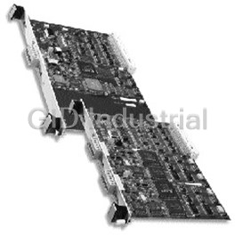
SST 5136-SD-VME
Description
SST 5136-SD-VME 5136-SD-VME Allen-Bradley DH/DH+ VME Card
Part Number
5136-SD-VME
Price
Request Quote
Manufacturer
SST
Lead Time
Request Quote
Category
PRODUCTS - 5
Specifications
Cable
Belden 9463, twinaxial, 20 AWG
Card Connector
Phoenix MSTB1.5/6ST-5.08
Card Type
5136-SD-VME-S
Consumed
from pins 32 of rows A, B, and C of the P1 connector
Current
1 A at 5V
Function
VMEbus scanner card for Allen-Bradley remote I/O network
Operating Humidity
5 to 95 % non-condensing
Operating Temperature
0-50 degrees Celsius
Storage Humidity
0 to 95%
Storage Temperature
0 -70 degrees Celsius
Datasheet

Extracted Text
5136-SD-VME-S User's Guide Version 1.03 50 Northland Road, Waterloo, Ontario N2V 1N3 (519) 725-5136 fax (519) 725-1515 ©1995-1998 S-S Technologies Inc. Printed in Canada 5136-SD-VME-S User's Guide Publication Name : SDVMES.DOC Publication Revision: 1.03 Date Printed: July 23, 1998 ©1995-1998 S-S Technologies Inc. --This Document Applies To -- 5136-SD-VME-S Remote I/O Scanner Interface Card ©1995-1998 S-S Technologies Inc. 5136-SD-VME-S User's Guide 1. INTRODUCTION ................................................... 1 1.1 Purpose of this Document............................................ 1 1.2 Card Overview ............................................................... 1 1.3 Manual Organization..................................................... 2 1.4 Conventions .................................................................. 2 1.5 Reference Documents................................................... 3 2. INSTALLATION .................................................... 5 2.1 Card Installation............................................................ 5 2.2 Setting the Switches and Jumpers .............................. 8 2.2.1 Setting the Short I/O Base Address........................... 8 2.2.2 Address Modifier Codes .......................................... 11 2.2.3 Setting the Interrupt ................................................ 11 2.2.4 Transmit Enable Jumper......................................... 12 2.2.5 SYSFAIL* Jumper................................................... 12 2.3 Short I/O Registers...................................................... 13 2.3.1 Control and Status Register .................................... 13 2.3.2 Interrupt Status/ID Register..................................... 15 2.3.3 Memory Address Register....................................... 16 2.4 Standard Address Space ............................................ 17 2.5 Diagnostic LEDs.......................................................... 17 2.6 Connecting to the Communication Network ............. 18 2.7 Loading a Program on the Card................................. 19 2.8 VME Programming Notes (READ THIS!!!!!) ............... 20 2.9 Software Modules ....................................................... 20 2.10 Card Options ............................................................. 21 2.11 Troubleshooting Installation .................................... 22 2.12 Related Products....................................................... 22 3. THE REMOTE I/O SCANNER MODULE ............ 23 i 5136-SD-VME-S User's Guide 3.1 Overview...................................................................... 23 3.2 Starting Up................................................................... 24 3.3 Configuring the Scanner ............................................ 24 3.3.1 Baud Rate............................................................... 24 3.3.2 Enabling Racks....................................................... 25 3.3.3 Installing Block Transfers ........................................ 26 3.3.4 Scan List................................................................. 29 3.3.5 Reconfiguration Flags ............................................. 29 3.4 Modes of Operation .................................................... 30 3.4.1 Program Mode ........................................................ 30 3.4.2 Run Mode ............................................................... 30 3.4.3 How to Change Mode.............................................. 31 3.5 Accessing I/O Data...................................................... 31 3.5.1 Discrete I/O Data .................................................... 31 3.5.2 Block Transfer Data ................................................ 32 3.6 Monitoring Operation.................................................. 35 3.6.1 COMM Flag ............................................................ 35 3.6.2 Ticker...................................................................... 35 3.6.3 Sync Byte ............................................................... 35 3.6.4 Scan Indicators ....................................................... 35 3.6.5 Rack Status Table................................................... 36 3.6.6 Error Counters ........................................................ 36 3.7 Event Processing ........................................................ 38 3.7.1 Types of Events...................................................... 38 3.7.2 Event Enable Mask................................................. 39 3.7.3 Event Flags and Tables .......................................... 39 3.8 Interrupts ..................................................................... 42 3.8.1 Types of Interrupts .................................................. 42 3.8.2 Interrupt Enable Mask ............................................. 43 3.8.3 Setting up for Interrupts........................................... 43 3.8.4 Interrupt Service Routine ........................................ 43 3.9 Watchdog..................................................................... 45 3.9.1 Enabling/Disabling the Watchdog............................ 45 3.9.2 Kicking the Watchdog ............................................. 45 3.9.3 Watchdog Timeout.................................................. 45 3.10 Summary of Memory Locations ............................... 46 3.11 Standard Header File................................................. 48 ii 5136-SD-VME-S User's Guide 3.12 Sample Programs on the Distribution Disk ............. 48 TECHNICAL DATA ................................................. 49 ACKNOWLEDGMENTS.......................................... 51 WARRANTY............................................................ 55 iii 5136-SD-VME-S User's Guide 1. Introduction 1.1 Purpose of this Document This document is a user's guide for the SST 5136-SD-VME-S remote I/O scanner for Allen-Bradley 1771 remote I/O. This card makes it possible for an application running on a VME host computer to communicate with and control Allen-Bradley 1771 remote I/O. 1.2 Card Overview The 5136-SD-VME-S interface card provides an intelligent front end between VMEbus master cards and an Allen-Bradley remote I/O network. The scanner is a co-processor card with circuitry to provide a standard bus interface to the VMEbus backplane. The card's form factor is double-height, single-width with electrical connection to the VMEbus backplane via the P1 connector. The card acts as a slave on the VMEbus. The scanner contains a Z180 processor which is loaded with software by the host computer to enable it to perform the communication tasks on the network. The card contains no software in ROM; the appropriate interface software is downloaded to the card from the host computer. Interaction between the task resident on the card and the application software on a VME host is made through shared memory. The lower 32 Kbytes of memory on the card are reserved for the software module which is downloaded when the card is initialized; the upper 32 Kbytes are used for data and tables. The card occupies a 64 Kbyte block of Standard Access space for the shared memory and a 6-byte "control block" in Short I/O space. (By definition, short addressing applies to boards which decode A01-A15. This mode of addressing is normally used for I/O boards. A16-A23 are not decoded; therefore the I/O memory is usually, but not always, mapped into the 64 Kbyte block $FF0000 to $FFFFFF.) The address of the control block is set using DIP switches on the card. 1 5136-SD-VME-S User's Guide There are three registers in the control block which affect the operation of the card: the control/status register, the interrupt status/ID register and the memory address register. All control block registers are 1 byte wide. The control/status register is a read-write register which allows the host to control and monitor the scanner. The interrupt status/ID register is used for interrupt initialization and processing. The memory address register is used to assign the address of the 64 Kbyte block of RAM associated with the scanner in the VMEbus standard access memory map. The card supports the VMEbus Priority Interrupt Bus. The interrupt vector is software selectable using the "Interrupt status/ID" register in the control block. The interface card generates interrupt requests using an I(1) through I(7) (Stationary), ROAK interrupter. D08(O) (Stationary) status/ID transfer capability is used. The card responds to Data D08(O) Transfer Bus (DTB) cycles in the A16 (Short) addressing mode and D16 or D08(EO) DTB cycles in the A24 (Standard) addressing mode. D08(EO) bus cycles are single-byte cycles. When 16-bit values are read from the card (i.e. buffer pointers) the values are organized in low-byte, high-byte order. The address modifier (AM) codes can be one of standard or short supervisory data access ($3D, $2D) or standard or short non-privileged data access ($39, $29). For diagnostic purposes the card is considered to be a "non-intelligent" card; diagnostic routines (i.e. memory test) are performed on the card by a master processor rather than by the card itself. 1.3 Manual Organization This document is divided into several sections: part 2 describes how to install the card, part 3 describes the scanner software and the steps in writing an application. The appendices give some technical information on the card and explain how to obtain technical support. 1.4 Conventions In this manual, a leading $ or 0x indicates a hexadecimal number. VMEbus signals are shown in bold. An asterisk indicates an active- low signal, for example SYSFAIL*. 2 5136-SD-VME-S User's Guide 1.5 Reference Documents Refer to the appropriate Allen-Bradley documents for information on Allen-Bradley hardware and cabling. Refer to “IEEE Standard for a Versatile Backplane Bus: VMEbus”, ANSI/IEEE Std. 1014-1987 for explanations of VMEbus terminology. 3 5136-SD-VME-S User's Guide 2. Installation The 5136-SD-VME-S interface card contains components that are sensitive to electrostatic discharge. Do not remove the card from its protective bag without using the following precautions: • Before handling the card, ground yourself by touching a grounded object, such as the case of your computer. • Never touch the backplane connectors or pins. Handle the card by its mounting bracket. • Always store the card in its protective bag. This chapter describes the procedures for: • setting the switches and jumpers on the interface card • installing the card in your computer • downloading the firmware to the card • getting the card to communicate on a network and verifying that it is working It also contains information about short I/O register usage on the card. 2.1 Card Installation Before you install the card in the VMEbus chassis, you must decide on the answers to the following questions: • which 1 Kbyte block in the Short address space will be used for card control? • will interrupts be used? • should the card respond to supervisory mode commands and data accesses only? In order to answer these questions, you must know the memory usage of the system and the capabilities of the application software. The answers to these questions determine the settings of the switches and jumpers on the card. These must be set before you install the card in a VMEbus computer. 5 5136-SD-VME-S User's Guide The table below shows the use for the various switch positions on the 10 position switch on the card and shows where to look for information on how to set the switch. Positions Used to set Reference section 1-6 Short I/O address 2.2.1 7 Allowed address modifiers 2.2.2 8-10 Interrupt 2.2.3 In addition there is a jumper which controls transmission from the card. Refer to section 2.2.4. The SYSFAIL* Jumper controls how the card handles the SYSFAIL* line. Refer to section 2.2.5. The following diagrams show the position of the switches, jumpers and LEDs on each of the cards. 6 5136-SD-VME-S User's Guide 5136-SD-VME-S 7 5136-SD-VME-S User's Guide 2.2 Setting the Switches and Jumpers 2.2.1 Setting the Short I/O Base Address The 1 Kbyte block of short address space occupied by the card is located on a 1Kbyte boundary at an address selected by positions 1 through 6 of the switch . These switch positions correspond to address bits A15 through A10, respectively, with a switch in the ON position matching the corresponding address signal as a 0. Switch Position Address bit 1 A15 2 A14 3 A13 4 A12 5 A11 6 A10 The following table shows possible addresses and the corresponding switch settings. Address 1 2 3 4 5 6 FC00 OFF OFF OFF OFF OFF OFF F800 OFF OFF OFF OFF OFF ON F400 OFF OFF OFF OFF ON OFF F000 OFF OFF OFF OFF ON ON EC00 OFF OFF OFF ON OFF OFF E800 OFF OFF OFF ON OFF ON E400 OFF OFF OFF ON ON OFF E000 OFF OFF OFF ON ON ON DC00 OFF OFF ON OFF OFF OFF D800 OFF OFF ON OFF OFF ON D400 OFF OFF ON OFF ON OFF D000 OFF OFF ON OFF ON ON CC00 OFF OFF ON ON OFF OFF C800 OFF OFF ON ON OFF ON 8 5136-SD-VME-S User's Guide Address 1 2 3 4 5 6 C400 OFF OFF ON ON ON OFF C000 OFF OFF ON ON ON ON BC00 OFF ON OFF OFF OFF OFF B800 OFF ON OFF OFF OFF ON B400 OFF ON OFF OFF ON OFF B000 OFF ON OFF OFF ON ON AC00 OFF ON OFF ON OFF OFF A800 OFF ON OFF ON OFF ON A400 OFF ON OFF ON ON OFF A000 OFF ON OFF ON ON ON 9C00 OFF ON ON OFF OFF OFF 9800 OFF ON ON OFF OFF ON 9400 OFF ON ON OFF ON OFF 9000 OFF ON ON OFF ON ON 8C00 OFF ON ON ON OFF OFF 8800 OFF ON ON ON OFF ON 8400 OFF ON ON ON ON OFF 8000 OFF ON ON ON ON ON 7C00 ON OFF OFF OFF OFF OFF 7800 ON OFF OFF OFF OFF ON 7400 ON OFF OFF OFF ON OFF 7000 ON OFF OFF OFF ON ON 6C00 ON OFF OFF ON OFF OFF 6800 ON OFF OFF ON OFF ON 6400 ON OFF OFF ON ON OFF 6000 ON OFF OFF ON ON ON 5C00 ON OFF ON OFF OFF OFF 5800 ON OFF ON OFF OFF ON 5400 ON OFF ON OFF ON OFF 5000 ON OFF ON OFF ON ON 4C00 ON OFF ON ON OFF OFF 4800 ON OFF ON ON OFF ON 4400 ON OFF ON ON ON OFF 4000 ON OFF ON ON ON ON 3C00 ON ON OFF OFF OFF OFF 9 5136-SD-VME-S User's Guide Address 1 2 3 4 5 6 3800 ON ON OFF OFF OFF ON 3400 ON ON OFF OFF ON OFF 3000 ON ON OFF OFF ON ON 2C00 ON ON OFF ON OFF OFF 2800 ON ON OFF ON OFF ON 2400 ON ON OFF ON ON OFF 2000 ON ON OFF ON ON ON 1C00 ON ON ON OFF OFF OFF 1800 ON ON ON OFF OFF ON 1400 ON ON ON OFF ON OFF 1000 ON ON ON OFF ON ON 0C00 ON ON ON ON OFF OFF 0800 ON ON ON ON OFF ON 0400 ON ON ON ON ON OFF 0000 ON ON ON ON ON ON 10 5136-SD-VME-S User's Guide 2.2.2 Address Modifier Codes The 5136-SD-VME-S provides 8-bit access to objects in its short address space, and 8- and 16-bit access to objects in its standard address space. Whether a particular bus cycle accesses short, standard, extended, or long (extended and long are not used on the 5136-SD-VME-S) address spaces, and the type of access that is made, are selected by the VME master through the use of the address modifier codes. These codes are decoded by the card and used to determine the object to be accessed. In addition to selecting from among the four spaces available on the VMEbus, address modifier codes also select whether the master is making a supervisory or non-privileged access, and (for all but short address space accesses) whether the access is to program or data space, and whether it is to be a single-object or block access. The 5136-SD-VME-S can respond to address modifier codes $3D, $39, $2D, and $29. This means that supervisory and non-privileged data accesses may be made to standard address space ($3D and $39), and that supervisory and non-privileged accesses may be made to short address space ($2D and $29). An access which can be positively determined to address the card, but with an address modifier code that is not supported, causes a VMEbus error. The selection of whether only supervisory accesses or both supervisory and non-privileged accesses are permitted is made with position 7 of the card’s DIP switch. The use of this switch is detailed in the following table. If a non-privileged access is made to the card when this switch is in the supervisory only position, a VMEbus error occurs. Switch position 7 Permitted accesses ON Both Supervisory and Non-privileged OFF Supervisory only 2.2.3 Setting the Interrupt If so enabled, the software module on the local processor can assert a VME interrupt on the switch-selected level. The level is set using positions 8, 9 and 10 of the corresponding switch block. 11 5136-SD-VME-S User's Guide Switch position Interrupt 8 9 10 ON ON ON none OFF ON ON 1 ON OFF ON 2 OFF OFF ON 3 ON ON OFF 4 OFF ON OFF 5 ON OFF OFF 6 OFF OFF OFF 7 2.2.4 Transmit Enable Jumper The jumper labelled TXENA is used to enable or disable transmission from the card. Transmission is disabled when the jumper is placed over the pins labelled DISA of the block. Transmission is enabled when the jumper is placed over the pins labelled ENA. The scanner must transmit so the jumper should be in the ENA position. 2.2.5 SYSFAIL* Jumper This jumper is labelled P6 on the 5136-SD-VME-S. When it is in the ON (right) position, assertion of the SYSFAIL* control bit in the control register causes the VMEbus SYSFAIL* signal to be asserted, the PASS LED to turn off, and the FAIL LED to turn on. When the jumper is in the OFF position, the LEDs reflect the state of the SYSFAIL* control signal but the card does not drive the VMEbus signal. 12 5136-SD-VME-S User's Guide 2.3 Short I/O Registers The card occupies 1 Kbyte of the short I/O space but only three 1-byte registers are used in that 1Kbyte area. The following table gives the map of the registers contained in the short address space to which the card responds. Since the short address space of the card is essentially a D08(O) Slave, the objects in this space are not at contiguous addresses. Any attempt to access addresses other than those specified in the table (e.g. offsets 0, 2 or 4), or to access objects larger than 8 bits from the card's short address space, results in a VMEbus error. Offset from short I/O base Selected register 1 Control and status register 3 Interrupt vector register 5 Memory address register 2.3.1 Control and Status Register The control and status register permits the host computer to: • enable/disable the local processor (Z180) • assert/deassert an interrupt to the local processor • sense and clear an interrupt from the local processor • control an indicator LED • assert/deassert the VME SYSFAIL signal from the card • enable/disable access to the card's shared RAM • enable/disable write protection to the local processor's code space The control and status register is located at offset 1 from the selected register base address in short address space. Its bits are all high true, and their assignments and reset states are detailed in the following table. 13 5136-SD-VME-S User's Guide Control/Status Register (byte at offset 1) BIT FUNCTION R/W RESET 0 local processor reset control R/W 1 1 interrupt to local processor R/W 0 2 clear interrupt from local W0 processor (reads as 0) 3 LED control R/W 0 4 SYSFAIL control R/W 0 5 shared RAM enable R/W 0 6 low 32KB write inhibit R/W 0 7 interrupt from local processor R 0 Setting the local processor reset control bit to '1' holds the processor on the card in reset and prevents it from running. Since this is the case following a system reset, the processor does not run until the host computer releases it, after the code has been loaded. When this bit is a '1' and the host writes a '0' to it, a reset pulse is issued to the Z180 on the card, causing it to begin execution at its own offset 0000. The interrupt to local processor bit is used by application software to get the attention of the module running on the Z180. This bit cannot be cleared by the local processor, so the host must clear it when it detects that the local processor has handled the interrupt. This interrupt is edge-sensitive. No current modules for the card use interrupts to the local processor. A status ID is placed on the bus during the interrupt acknowledge cycle, as specified in the Interrupt ID register. The local processor generates an interrupt by setting the interrupt from local processor bit, which causes the selected VME interrupt signal to be asserted. This signal is released when the interrupt acknowledge cycle takes place, but the interrupt from local processor bit that caused that interrupt remains set until cleared explicitly by an interrupt service routine. The routine must do this by writing a '1' to the clear interrupt from local processor bit, which clears and re-enables the hardware for further interrupts. The LED control bit turns on (1) and off (0) the RUN LED for the card. (The STATUS LED is controlled by the local processor directly and is used by the software as an indicator of its current state.) 14 5136-SD-VME-S User's Guide Setting the SYSFAIL control bit to '1' asserts the SYSFAIL* signal on the VMEbus if the SYSFAIL jumper is in the "ON" position. This bit also controls the state of the PASS and FAIL LEDs on the card. Following reset, the shared RAM enable bit assures that the card will not drive the VMEbus for any standard address cycles. This bit must not be set to '1', enabling access to the shared RAM, until the Memory address register has been set to the required base in standard address space. Since all of the Z180's memory is shared with the VME host, it may be desirable to prevent the host from writing to the lower 32 Kbytes of Z180 memory. SST software uses the lower 32 Kbytes for Z180 code and unintentional writes to this area by the host could cause the Z180 software module to crash. The low 32KB write inhibit bit, when '1', prevents host-initiated write cycles from altering shared RAM in the range $0000 to $7FFF (offset from the selected standard access base). Such cycles do not cause VMEbus errors and appear to complete normally. Nevertheless, as with all shared RAM cycles, they should be minimized as they rob cycles from the local processor. Whenever the card software generates an interrupt, it sets the interrupt from local processor bit. 2.3.2 Interrupt Status/ID Register When an interrupt request is made from the card on one of the VME interrupt lines, an interrupt handler acquires the bus and executes an interrupt acknowledge cycle. The card recognizes the acknowledgment and places an 8-bit interrupt ID on the odd half of the data bus. The value for this ID is taken from the Interrupt ID register, located at offset 3 from the selected register base address in short address space. This register is zeroed by system reset and may be read or written at any time. If interrupts are used from the card, this register should be initialized before the local processor is allowed to run. 15 5136-SD-VME-S User's Guide 2.3.3 Memory Address Register Following system reset, the shared RAM enable bit in the Control/Status register is reset, preventing the card from driving the bus during any standard address cycles. This is done in order that the location in standard address space occupied by the shared RAM may be selected. Standard address space accesses use 24 bits of address (16MB) while the card uses only 16 bits of address (64 Kbytes) for generating addresses into the shared RAM. For standard address bus cycles, the upper 8 bits from the VMEbus are compared to the bits in the 8-bit Memory address register, located at offset 5 from the selected register base address in short address space. If these match exactly, and the shared RAM enable bit is set, then a shared RAM access is performed. For example, if it is required that the shared RAM occupy the 64 Kbyte block between $0D0000 and $0DFFFF in standard address space, then the Memory address register should be set to $0D. The memory address register is zeroed by system reset, and may be read or written at any time. It should be initialized with the upper 8 bits of the 24-bit address at which the shared RAM area is to begin. 16 5136-SD-VME-S User's Guide 2.4 Standard Address Space The card contains 64 Kbytes of static RAM that is used as the code and data memory for the local processor (Z180) and the tables and registers for all network activity in which the card is involved. This RAM is accessible at any time to a master on the VMEbus, regardless of whether or not the local processor is running. As necessary, the local processor pauses while the VMEbus master accesses the memory. This memory is located at offsets $0000 through $FFFF from the 24-bit base address, whose upper 8 bits are determined from the Memory Address register contents. A VME master may access the memory either 8 or 16 bits at a time. If a 16-bit object is accessed, it must be aligned on a 16-bit boundary. That is, an access to a 16-bit object, 8 bits of which are in the odd byte of one address, and whose other 8 bits are in the even byte of the next address, is not possible. If this is attempted by host software, the hardware on the master will probably take care of the details, performing two single-byte accesses invisibly to the software. Byte addresses on the VMEbus access locations that correspond exactly to addresses on the local processor. Also, 16-bit accesses on the VMEbus access the expected bytes from the local processor's space. For example, if $1234 is written by a VMEbus master to offset 0 in the shared RAM, the local processor sees $12 at address 0, and $34 at address 1. Since the processor on the card puts low bytes at low addresses and VMEbus masters put low bytes at high addresses, care must be taken when accessing 16-bit objects in the shared RAM to ensure that the byte ordering is what the software (and local processor) expect. 2.5 Diagnostic LEDs The PASS and FAIL LEDs provide information on the overall operation of the card. They follow the state of the SYSFAIL line when the SYSFAIL jumper is in the ON position. See section 2.2.5. In addition, there are two diagnostic LEDs on the card. The red RUN LED is controlled by application software using the card's control register. This allows a host processor to perform diagnostics on the card and manipulate the state of the LED to give an indication of the results. 17 5136-SD-VME-S User's Guide The green STATUS LED is under control of the microprocessor on the card. It is on whenever racks have been enabled in the scanner. 2.6 Connecting to the Communication Network The scanner has been designed to provide direct connection to Allen-Bradley programmable controller communication networks. Allen-Bradley specifies Belden 9463 twinaxial cable ("Blue Hose") for their network installations. The Blue Hose is wired into the scanner using the Phoenix Combicon connector supplied with the scanner. See page 49 for the part number of the connector. For wiring purposes pin 1 of the Phoenix connector is identified on the faceplate of the scanner and is the bottom pin. Pins 1, 2 and 3 are connected internally to pins 4, 5 and 6, respectively. Connect Pin 1 to the Line 1 of the remote I/O network. This is usually, but not always, the blue wire. Connect Pin 2 to the shield. Connect Pin 3 to Line 2. This is usually, but not always, the clear wire. Termination The nodes at the two physical ends of the network should have terminating resistors. All other nodes should not. Every network should have exactly two terminators. The card does not have an onboard terminator. If you require a terminator, it consists of a resistor between the blue and clear wires. Allen-Bradley recommends an 82 ohm resistor unless you have older devices on the network that require 150 ohm resistors. Refer to Allen-Bradley documentation for further details. 18 5136-SD-VME-S User's Guide 2.7 Loading a Program on the Card An application must take the following steps to initialize the interface card. 1. Make sure the processor is reset by writing to the control/status register. Select the card address by writing to the address register. 2. Enable card memory by setting the enable bit in the control register. 3. If interrupts are to be used, initialize the interrupt status/ID register. 4. Perform memory test etc. as required by the application. 5. Set or clear the RUN LED according to the result of the memory test. 6. Load the software module SDRMAS.BIN onto the card at the standard memory address. That is, read the file SDRMAS.BIN and write it the memory on the scanner, starting at the base address. Verify that the module has been correctly loaded. 7. Write $A5 into offset $8000 from the start of memory. 8. Set the run bit in the control register. 9. Look at the byte at offset $8000. Wait up to 7 seconds for it to change. If it doesn't change, the module did not run on the card. If it becomes 00, everything has run correctly. If it becomes 01, there is a null-terminated string starting at offset $8001 which describes the error. If it has any other value, the result is invalid and the processor did not run correctly. 10. Run your application. The distribution disk contains a sample loader for a Xycom XVME computer. 19 5136-SD-VME-S User's Guide 2.8 VME Programming Notes (READ THIS!!!!!) The following information should always be kept in mind when reading the module descriptions. The tables on the card are all memory mapped. Within the 64K of card memory, the lower 32 Kbytes are reserved for the card software; the upper 32 Kbytes are used by the tables by which the host application communicates with the card. The card processor organizes data in low-byte/high-byte format. Your application must take this into consideration. For example, messages are placed into buffers at locations given by the card software. When your application reads the card to determine the location of the next free buffer and the bytes read are sequentially $00 and $0A, the next free buffer is at offset $0A00 from the start of the data area (rather than $000A as you might expect in a VMEbus environment.) The tables on the card contain some elements that are one byte wide. Some compilers by default align structure elements on word boundaries; you must tell your compiler to use byte alignment for structure elements that refer to data on the card. 2.9 Software Modules The following modules are shipped with the 5136-SD-VME-S. Module Purpose sddopt.bin module to display card options sdrmas.bin module to scan remote I/O. 20 5136-SD-VME-S User's Guide 2.10 Card Options The 5136-SD-VME-S contains an EEPROM that is programmed before the card is shipped to select which software modules the card can run. Possible options include: DH Data Highway DHP Data Highway Plus MON Data Highway Plus monitoring (for DH+ Network Analyzer) NET network monitor (for DH+ Network Analyzer) KTEMU KT emulation EXEC the exec module RIO for emulating remote I/O. For use on the 5136-SD-VME-R card. Requires a licence from Allen-Bradley. Contact SST for details. RMAS for scanning remote I/O. For use on the 5136-SD-VME-S card The 5136-SD-VME-S is shipped with just the RMAS option enabled. To determine what options are enabled on your card, load the card module SDDOPT.BIN. The module simply reads the options enabled and displays them at offset $8001, then sets $8000 to 01 (same as an error). If you try to load a module for which the option is not enabled, the module puts the message "*** Fatal Error ; Option Not Enabled on this Card ***" at location $8001, $8000 gets set to 01 (same as an error) and the module does not run. 21 5136-SD-VME-S User's Guide 2.11 Troubleshooting Installation This section describes what to do if the card cannot communicate on a network. It also provides more detailed information on some common sources of problems. • Check cabling for correct wiring to the card. • Check for shorted wires, leads on terminating resistors shorted to cables, strands from the shield shorting to the other wires. • Check baud rate • Check network termination. Only the two nodes at the physical ends of the network should have terminating resistors. 2.12 Related Products SST produces the following related products: 5136-SD ISA bus card for DH/DH+ 5136-SD-VME-R VMEbus card which emulates and monitors remote I/O 5136-SD-VME-S VMEbus remote I/O scanner 5136-SD-MUL Multibus I card for DH/DH+ 22 5136-SD-VME-S User's Guide 3. The Remote I/O Scanner Module 3.1 Overview The Remote Master (SDRMAS) software module permits an application running on a host VME computer to drive Allen-Bradley 1771 remote I/O. The software module uses tables in memory which represent the status of digital inputs and outputs. These tables are organized to correspond to the rack, I/O group, slot and bit address of digital I/O points. The SDRMAS module continuously updates the tables by reading the status of inputs from the remote I/O network and writing output values to the remote I/O network. When an application requires input information, it reads from the memory locations assigned in the tables. An application wishing to manipulate outputs writes the output bits to the appropriate area in the output tables. SDRMAS can also perform block transfer reads and writes with modules in remote racks. SDRMAS can be configured to drive up to 32 physical racks over the remote I/O network. The software supports half or quarter racks with the restriction that each rack must start on a full rack boundary; in other words, the starting I/O group must be zero and each rack must have a unique rack number. The program uses the PLC-3/5 message format (important for setting adapter and rack switches) and can operate at baud rates of 57.6, 115.2 or 230.4 Kbaud. Rack 0 can be a remote rack. Operation of the scanner on the network is transparent to the application program. The application reads and writes memory locations to set the baud rate, to enable racks for communication, to obtain the current status of those racks, to update the values of inputs and outputs, and to perform block transfers. 23 5136-SD-VME-S User's Guide Applications interact with SDRMAS through data tables and flags in the shared memory. The addresses of these locations are given as offsets into the upper 32 Kbyte area of the memory occupied by the scanner card. For example, if the scanned is configured to occupy the 64 Kbytes of memory stating at 0xD0000, the lower 32 Kbytes (0xD0000-0xD7FFF) is used for the SDRMAS software itself and the tables area occupies 0xD8000-0xDFFFF. An offset of 0x801 in this manual is an offset into the upper 32 Kbytes and refers to address 0xD8801. All offsets are in the range 0 to 0x7FFF. 3.2 Starting Up Refer to section 2.7 for the procedure to follow to install a software module on the scanner. The three CHK bytes at offsets 0x80B-0x80D are used to indicate when you can begin to access the scanner. These three bytes contain 0xC3, 0x04 and 0xAA respectively. They are written by SDRMAS to these locations when it is ready to begin operation. Your application should check these three bytes for the correct values before it attempts any other operations on the scanner. See section 3.10 for a complete summary of memory locations. 3.3 Configuring the Scanner Before you can scan remote I/O, you must set various parameters to tell SDRMAS about the network. These include the network baud rate, the racks being scanned and, optionally, if you want to use a scan list. Block transfers can be installed at any time but you may prefer to install them during initial configuration of the system. 3.3.1 Baud Rate Communication between the scanner and remote racks takes place at one of three possible baud rates. The baud rate at the scanner must match that set by the switches on the various remote I/O adapters on the network. 24 5136-SD-VME-S User's Guide The BAUD_RATE byte, at offset 0x801, and the BAUD_230 byte, at offset 0x802, are used to indicate to SDRMAS the baud rate which is being used for communication between the scanner and remote racks. SDRMAS defaults to 115.2 kbaud. Baud BAUD_230K BAUD_RATE 57.6K 0 0 115.2K 0 0xFF 230.4K 0xFF 0xFF If you change the baud rate, you must reconfigure SDRMAS (see section 3.3.5) before the changes take effect. 3.3.2 Enabling Racks The active rack table (RACK_ENABLE), at offsets 0x2C00-0x2C1F, is used to tell SDRMAS which racks are to be scanned. Note that the rack must start on a full rack boundary; that is, at starting I/O group 0. Each byte in this table corresponds to one rack. Writing 0xFF to a location tells SDRMAS to scan that rack. As an example, to activate rack 2, write 0xFF to location 0x2C02. SDRMAS then scans the rack and enters the rack size in the rack length table (RACK_END), at offsets 0xC00 - 0xC1F. There is one byte per rack in this table. The entries in the rack length table can be: Value Rack size 00 1/4 rack 01 1/2 rack 10 3/4 rack 11 full rack SDRMAS also enters the rack status in the rack status table (see section 3.6.5) at this time. The length is valid only if the rack status is active; that is, if the rack status is PROGRAM or RUN. For example, if the baud rate is incorrect, SDRMAS cannot communicate with the rack to determine its size. 25 5136-SD-VME-S User's Guide 3.3.3 Installing Block Transfers SDRMAS can initiate block transfers with remote racks. Before a block transfer can be performed, there are several tables into which you must enter data about the block transfer. There are two sets of tables, one for block transfer reads and one for block transfer writes. The tables are organized on the basis of rack, I/O group and slot. SDRMAS has a large pool of free memory from which you allocate space for the data for each block transfer. This memory occupies offsets 0x3000 to 0x7EFF. Your application must allocate some of this memory for each block transfer you use and tell SDRMAS where it is. The number of block transfers is limited only by the size of this pool. The block transfer location table tells SDRMAS where to find the data for a given block transfer (rack, I/O group and slot). The block transfer length table tells SDRMAS how many words long the block transfer is. SDRMAS does not check the values you write into the location and length tables; you must ensure that the memory allocated for a specific block transfer does not overlap the data for any other block transfer. Block transfers can be initiated on a one-time basis or on a timed, continuous basis. The block transfer update time table tells SDRMAS how often the block transfer should be executed. There are no limits on the number of block transfers that can be enabled at any time. The update time is the number of I/O scans between the completion of the block transfer and the start of the next block transfer. If multiple block transfers are enabled on a rack, the number is treated as the minimum number of scans; the actual number of scans may be longer and depends on the other block transfers that are enabled on that rack. If the order of execution of the block transfers is important, you should not used timed block transfers; you should execute them manually from your application. Refer to section 3.5.2. Table BTR BTW Location 0x1000-0x13FF 0x2000-0x23FF Length 0x1800-0x19FF 0x2800-0x29FF Update time 0x1A00-0x1BFF 0x2A00-0x2BFF 26 5136-SD-VME-S User's Guide To enable a block transfer, first write to the location table, then to the length table and finally to the update time table. Block Transfer Reads Block Transfer Reads use the BTR_LOC, BTR_LEN and BTR_TIME tables. The BTR_LOC table is located at offsets 0x1000 to 0x13FF and is organized by rack, I/O group and slot, with two bytes for each possible module location. It contains the offset to the start of the block transfer data in the block transfer data area. The data must be written in Least Significant Byte-Most Significant Byte (LSB-MSB) format. For a particular module with block transfer capability, the location in the BTR_LOC table is given by: BTR_LOC = 0x1000 + (RACK * 32) + (IOGROUP * 4) + (SLOT * 2) The BTR_LEN table is located at offsets 0x1800 to 0x19FF and is organized by rack, I/O group and slot, with one byte for each possible module location. It contains the length of the data (number of words) in the lower six bits and two control/status bits (bits 6 and 7). For a specific module, the location in the length table is given by: BTR_LEN = 0x1800 + (RACK * 16) + (IOGROUP * 2) + SLOT In addition, continuous block transfer reads use the BTR_TIME table at offsets 0x1A00 - 0x1BFF. This table is organized just like the length table. The location in the update time table is given by: BTR_TIME = 0x1A00 + (RACK * 16) + (IOGROUP * 2) + SLOT A block transfer read is non-continuous if the BTR_TIME is 0. Example: An analog input module is located in rack 3, I/O group 2, slot 1. The pointer to the block transfer read data is stored at: BTR_LOC = 0x1000 + (RACK * 32) + (IOGROUP * 4) + (SLOT * 2) BTR_LOC = 0x1000 + (3 * 32) + (2 * 4) + (1 * 2) BTR_LOC = 0x1000 + 96 + 8 + 2 BTR_LOC = 0x1000 + 106 27 5136-SD-VME-S User's Guide BTR_LOC = 0x1000 + 0x6A BTR_LOC = 0x106A The length of the block transfer read is stored at: BTR_LEN = 0x1800 + (RACK * 16) + (IOGROUP * 2) + SLOT BTR_LEN = 0x1800 + (3 * 16) + (2 * 2) + 1 BTR_LEN = 0x1800 + 48 + 4 + 1 BTR_LEN = 0x1800 + 53 BTR_LEN = 0x1800 + 0x35 BTR_LEN = 0x1835 If you want the block transfer to be 6 words long and the data to start at offset 0x3080, write 0x80 and 0x30 to offsets 0x106A and 0x106B respectively and write 0x06 to offset 0x1835. When you execute the block transfer read (by writing 0x46 to 0x1835), the data will be written to the 6 words (12 bytes) beginning at offset 0x3080. If the block transfer is to be continuous, put the update time at offset 0x1A35. Once the block transfer is enabled (see section 3.5.2), SDRMAS reschedules it periodically. Block Transfer Writes Block Transfer Writes use the BTW_LOC and BTW_LEN tables. These tables are similar in organization to the tables for block transfer reads. The BTW_LOC table contains pointers into the block transfer data area. This table is located at offsets 0x2000 to 0x23FF. For a particular module with block transfer capability, the location in the BTW_LOC table is given by: BTW_LOC = 0x2000 + (RACK * 32) + (IOGROUP * 4) + (SLOT * 2) The data must be written in Least Significant Byte-Most Significant Byte (LSB-MSB) format. The BTW_LEN table, at offsets 0x2800 to 0x29FF, contains the length of the data (number of words) of the block transfer write. The location in the length table is given by: BTW_LEN = 0x2800 + (RACK * 16) + (IOGROUP * 2) + SLOT 28 5136-SD-VME-S User's Guide In addition, continuous block transfer writes use the BTW_TIME update time table at offsets 0x2A00-0x2BFF. The location in the time table is given by: BTW_TIME = 0x2A00 + (RACK * 16) + (IOGROUP * 2) + SLOT A block transfer write is non-continuous if the BTW_TIME is 0. 3.3.4 Scan List By default, SDRMAS scans racks in rack number order, using the active rack table. However, provision has been made to let you use a scan list if your application requires it. The scan list can contain up to 31 racks. Racks can be duplicated in the scan list if some racks require more frequent servicing. The SCAN_LIST table is located at offsets 0x2C20-0x2C3F. If you are using the scan list, the first byte in this table must be 0xFF. Otherwise, it must be 0. Each element in the table is the rack number of a rack to be scanned. The end of the list should be marked with another 0xFF if there are fewer than 31 racks in the list. You do not need the final 0xFF if the list contains 31 racks. The scan list pointer (SCAN_LIST_PTR), at offset 0x805, shows which element in the list is currently being scanned at any given time. It ranges from 1 (first element in the list) to whatever the final element is. The current rack byte (CURR_RACK), at offset 0x804, shows the rack number of the rack being scanned, whether or not you are using a scan list. 3.3.5 Reconfiguration Flags SDRMAS uses two flags to perform the handshaking when you do a reconfiguration. The Configuration byte (CONFIG), at offset 0x803, is used to reconfigure the SDRMAS Software. Data tables are cleared and the hardware is reinitialized. The Configuration done byte, (CONFIG_DONE), at offset 0x822, is used to tell SDRMAS you've finished entering configuration data. The baud rate is set and racks begin to be scanned. The procedure is: 29 5136-SD-VME-S User's Guide • clear CONFIG_DONE to zero • set the CONFIG byte to 0xFF and wait for SDRMAS to clear it to zero. • enter the configuration data such as baud rate, racks to be enabled, block transfers, and so on. • set CONFIG_DONE to 0xFF to tell SDRMAS you've finished. After a reconfiguration, SDRMAS is in program mode. The sample program RMASCNF.C shows how to configure I/O and start the card. 3.4 Modes of Operation SDRMAS has two modes of operation - program mode and run mode. The remote rack responds just as it would if it were being driven by a programmable controller and the mode was program or run. 3.4.1 Program Mode In program mode: • output information is sent to the remote racks • all module outputs are off • discrete inputs are updated • block transfers are not performed 3.4.2 Run Mode In run mode: • output information is sent to the remote racks • discrete inputs are updated • block transfers are performed • outputs are allowed to energize 30 5136-SD-VME-S User's Guide 3.4.3 How to Change Mode The mode of operation is controlled by the MODE byte (offset 0x800). This location is used to indicate to SDRMAS whether to update the racks in program mode or run mode. A value of 0 indicates program mode; 0xFF indicates run mode. The mode can be changed at any time but block transfers stop when SDRMAS is in program mode. 3.5 Accessing I/O Data 3.5.1 Discrete I/O Data Digital Outputs: Offsets 0x000 - 0x1FF (OUTPUT) Each bit in this table corresponds to an output bit in a rack. Each word (two bytes) corresponds to the outputs for one I/O group in a rack, e.g. the sixteen bytes from 0x000 to 0x00F give the state of the outputs for rack 0. The bytes are organized in low-byte, high-byte format so address 0x000 contains the low bits and 0x001 contains the high bits for the first rack, I/O group zero. After an application writes the desired outputs to this table they are transmitted to the remote racks when SDRMAS scans the rack.The following formula is used to determine the address of a particular output word: OUTPUT_ADDR = (RACK * 16) + (IOGROUP * 2) where the rack, iogroup and constants (16 and 2) are expressed in decimal. Example: Rack 2 outputs are found in locations 0x20 to 0x2F. The outputs for I/O group 2 would be placed at: OUTPUT_ADDR = (2 * 16) + (2 * 2) = 32 + 4 = 0x24 that is, at 0x24 (low byte) and 0x25 (high byte). 31 5136-SD-VME-S User's Guide Digital Inputs: Offsets 0x400 - 0x5FF (INPUT) Each bit in this table corresponds to an input bit in a rack. Each word (two bytes) corresponds to the inputs for one I/O group in a rack, e.g. the sixteen bytes from 0x400 to 0x40F give the state of the inputs for rack 0. The bytes are organized in low-byte, high-byte format so address 0x400 contains the low bits and 0x401 contains the high bits for the first rack, I/O group zero. This table is built by the SDRMAS software using messages it receives from the racks. The following formula is used to determine the address of an particular input word: INPUT_ADDR = 0x400 + (RACK * 16) + (IOGROUP * 2) where the constants (16 and 2) are expressed in decimal. Example: Rack 2 inputs are found in locations 0x420 to 0x42F. The inputs for I/O group 2 are found at: INPUT_ADDR = 0x400 + (2 * 16) + (2 * 2) = 0x400 + 32 + 4 = 0x424 that is, at 0x424 (low bits) and 0x425 (high bits). To find the state of a specific input bit, determine the address and read the memory at that location, then mask off the required bit. 3.5.2 Block Transfer Data Enabling Block Transfers To enable a block transfer, the following steps must be taken: 1. Enter an address for the data to come from if it's a block transfer write or to go to if it's a block transfer read. Block transfer memory is from 0x3000 up to 0x7EFF. Your application must write the address into the BTR_LOC or BTW_LOC table. 2. If a block transfer write is to be initiated, the data to be written should be put into the block transfer data buffer. 3. The length byte (BTR_LEN & BTW_LEN) is used as follows: 32 5136-SD-VME-S User's Guide 76543210 CMD/STS BT Length Bits 0 to 5 are used to define the length of the block transfer. (For a length of 64, enter 0). Bits 6 and 7 are used as status bits. Status Set By Meaning 0 Block transfer not enabled. 1 HOST Initiate block transfer. Set by host along with length to start the block transfer. 2 SDRMAS BT done. Set by SDRMAS to indicate that the block transfer write data has been written or that the block transfer read data has been read and is available 3 SDRMAS BT error. The remote rack did not respond to the block transfer request. 4. If the transfer is a block transfer read, when the BT status indicates the block transfer has completed successfully, the data can be read from the block transfer read buffer. Example: A 10-word block transfer read is to be executed from rack 4 I/O group 3 slot 1. The data is to be stored at 0x3000. BTR_LOC = 0x1000 + (rack * 0x20) + (mod_grp * 4) + (slot * 2) = 0x1000 + (4 * 0x20) + (3 * 4) + (1 * 2) = 0x1000 + 0x80 + 0x0C + 2 = 0x108E So at 0x108E we would put the word value 0x3000, in low-byte high- byte format i.e. 0x00 at 0x108E and 0x30 at 0x108F. BTR_LEN = 0x1800 + (rack * 0x10) + (mod_grp * 2) + (slot) = 0x1800 + (4 * 0x10) + (3 * 1) + (1) = 0x1800 + 0x40 + 6 + 1 = 0x1847 33 5136-SD-VME-S User's Guide In the BTR_LEN table entries, the lower 6 bits are 0x0A for the length of 10. To initiate the block transfer read, the command 01 is put in bits 6 and 7. Therefore writing 0x4A to the location 0x1847 in the BTR_LEN table initiates the block transfer read. The host then waits for the status bits to change from 1 to 2 or 3. If the status is 2 (0x08A in BTR_LEN) then the BTR is complete and the data is in the block transfer buffer starting at the address in the location table (0x3000). If the status is 3 (0x0CA), the block transfer was in error. Block transfer writes are handled the same way, except the data must be put into the buffer at the location pointed to in the BTW_LOC table before the block transfer is initiated. If the block transfer is a timed block transfer, SDRMAS uses the value in the update time table to periodically reschedule the block transfer. Once you enable the block transfer, it continues until an error occurs or until you enter zero in the update time table for that block transfer. Possible causes of block transfer errors • The address in the BT_LOC table is not correct, or not at the right place in the table. • The rack is not responding (check the rack status table at 0x1C00). • The location (rack, I/O group, slot) does not contain a module which responds to block transfer requests. • The module is not responding to the block transfer request. • You are writing to the output table at the location occupied by the block transfer module. NOTE: if an attempt is made to initiate a block transfer to a rack which is not enabled, the status of the block transfer remains 01 since SDRMAS never checks disabled racks for block transfers. 34 5136-SD-VME-S User's Guide 3.6 Monitoring Operation SDRMAS contains several flags and tables which your application can monitor to determine the state of communication with remote racks. 3.6.1 COMM Flag The COMM byte, at offset 0x824, is set by SDRMAS to indicate that racks are responding and is used for testing communication on the network. A value of 0 indicates that at least one rack is in error; a value of 0xFF indicates all racks are responding. The status of an individual rack is available in the Rack Status Table. (See section 3.6.5) 3.6.2 Ticker The TICKER byte, at offset 0x806, can be used as an indication that the scanner software is running. The value should be constantly incrementing. If your application reads the same value from this location on successive reads, it indicates problems with the scanner. Note that the operation of the ticker has nothing to do with the mode of operation of SDRMAS; it increments in either program or run mode. It is intended to be used as an indication of the health of the SDRMAS software itself. 3.6.3 Sync Byte The SYNC byte, at offset 0x807, is cleared by SDRMAS when it reaches the end of the enabled racks and starts a new scan. This is true whether you've enabled the racks by using the active rack table or if you're using a scan list. The SYNC byte can be used by your application to synchronize with the SDRMAS I/O scan. Set this byte to a non-zero value; when SDRMAS clears it, you know the scan has been completed. 3.6.4 Scan Indicators The current rack byte (CURR_RACK), at offset 0x804, shows the rack number of the rack being scanned, whether or not you are using a scan list. If you are using a scan list, the scan list pointer (SCAN_LIST_PTR), at offset 0x805, shows which element in the scan list is currently being scanned at any given time. It ranges from 1 (first element in the list) to whatever the final element is. 35 5136-SD-VME-S User's Guide 3.6.5 Rack Status Table In the RACK_STATUS Table, at offsets 0x1C00 - 0x1C1F, each byte corresponds to one rack. The table is built by the SDRMAS software from messages on the remote I/O line. The contents reflect the status of each rack. Possible entries are: 0 Rack is not enabled. 1 The rack is presently being updated in RUN mode. 2 The rack is presently being updated in PROGRAM mode. 3 rack error. This rack is not responding. 3.6.6 Error Counters SDRMAS has several error counters to monitor operation on the network. The counters are organized on a rack-by-rack basis, one byte per rack. These counters increment up to 0xFF and then remain at 0xFF. Your application is free to clear these counters at any time. Rack Timeouts, offsets 0x1C20 - 0x1C3F (RACK_TOUTS) If a rack does not reply to a message from SDRMAS within a certain time, SDRMAS increments the corresponding rack time-out counter and retries the message once. If the rack still does not reply, SDRMAS increments the rack time-out counter again, then increments the rack failure counter for that rack, changes the status of that rack in the rack status table to rack error and, on the next scan, sends an initialization message to the rack. CRC Errors, offsets 0x1C40-0x1C5F (RACK_CRC_ERRS) If a message with a bad CRC is received from a rack, SDRMAS increments the corresponding counter in this table and retries the message once. If the rack still does not reply correctly, SDRMAS increments the CRC error counter again, then increments the rack failure counter for that rack, changes the status of the rack in the rack status table to rack error and, on the next scan, sends an initialization message to the rack. 36 5136-SD-VME-S User's Guide Rack Failures, offsets 0x1C60-0x1C7F (RACK_FAILURES) If SDRMAS puts a rack into error, for whatever reason, it increments the corresponding counter for that rack in this table. Protocol Errors, offsets 0x1C80-0x1C9F (RACK_PRTCL_ERRS) If SDRMAS receives an invalid response from a rack, it increments the corresponding counter in this table and retries the message once. If the rack still does not reply correctly, SDRMAS increments the protocol error counter again, the increments the rack failure counter for that rack, changes the status for the rack in the rack status to rack error and, on the next scan, sends an initialization message to the rack. Block Transfer Errors, offsets 0x1CA0-0x1CBF (RACK_BT_ERRS) If SDRMAS enables a block transfer and the rack does not respond to the block transfer request within 100 scans of that rack, SDRMAS increments the corresponding counter for that rack in this table and sets the status of that block transfer to error. Block Transfer Protocol Errors, offsets 0x1CC0-0x1CDF (RCK_BT_PRT_ERRS) If SDRMAS receives an invalid message from a rack during execution of a block transfer, it increments the corresponding counter for that rack in this table. The block transfer protocol error counters also increment if SDRMAS receives unsolicited block transfers. These are usually caused when your application inadvertently writes outputs to a location occupied by a block transfer module. 37 5136-SD-VME-S User's Guide 3.7 Event Processing SDRMAS contains a system whereby you can monitor for various occurrences such as rack errors, data changes and so on. It is implemented as a chain of flags which makes it possible to determine quickly the type and location of the event. A single flag indicates when any event occurs. Various event flags show which type of event has occurred. Event tables show which rack the event occurred on. By using this chain of flags, your application can quickly pinpoint the event and process the event data. Events are maskable. You can include or exclude particular types of events by writing to the Event Enable mask byte. 3.7.1 Types of Events Rack Errors A rack error event occurs when a rack goes into error. Input Data Change An input data change event occurs when any discrete input data for any rack changes. Block Transfer Read Event For continuous block transfers, a block transfer read event occurs when there's either a data change in the data being read or when there's a block transfer read error. For non-continuous block transfers, a block transfer read event occurs when the block transfer data has been received or when an error occurs. Block Transfer Write Event For continuous block transfers, a block transfer write event occurs when there's a block transfer write error. For non-continuous block transfers, a block transfer write event occurs when the reception of the block transfer data has been acknowledged by the remote rack or when there's a block transfer write error. Watchdog Time-out A watchdog time-out event occurs when the watchdog timer has been enabled and times out. 38 5136-SD-VME-S User's Guide 3.7.2 Event Enable Mask The Event Enable mask byte (EVENT_ENABLE), at offset 0x819, is used to enable or disable routing of the various types of events to the master EVENT_FLAG. Each bit in this byte corresponds to a different type of event. Bit Event type 0 Rack errors 1 Discrete input change 2 Block transfer read 3 Block transfer write 4 Scan done Watchdog time-out events are not maskable. When the bit is set, the event type is routed to the EVENT_FLAG. The default is for all event types except the watchdog time-out to be disabled. 3.7.3 Event Flags and Tables There are several event flags which are used to indicate which type of event has occurred. The EVENT_FLAG, at offset 0x818, is set whenever any non-masked event occurs. When your application sees this flag set, it should first clear the flag so that new events can be detected, then begin the search for the type and location of the event. Your application should first search through the various event type flags to determine the event type. When it finds one of them set, it should clear the flag so that a new event can be detected, then search the corresponding event table to determine where the event occurred. The rack error flag (RACK_ERROR_FLG), at offset 0x810, is set when a rack goes into error. First clear the rack error flag, then search the rack status table to determine which rack is in error. 39 5136-SD-VME-S User's Guide The Input change flag (INPUT_CHG_FLG), at offset 0x811, is set when discrete input data has changed. To determine where the data change occurred, scan the RCK_IN_CHNGE table at offsets 0x1D00 to 0x1D1F. The rack where the data changed is the one with the corresponding byte set to 0xFF. Clear the flag, then read the input data for that rack. Note that multiple data change events may occur so the RCK_IN_CHNGE table should be searched even if one event has already been found. The BTR Event flag (BTR_EVENT_FLG), at offset 0x812, is set when a block transfer read event has occurred. To determine where the block transfer read event occurred, first clear the flag so that other block transfer read events can be detected, then scan the rack block transfer read event table (RCK_BTR_EVENT), at offsets 0x1D20- 0x1D3F, to determine which rack generated the event. Locate the byte which is set and clear it so that new block transfer read events can be detected, then scan the block transfer read event table (BTR_EVENT), located at offsets 0x1400-0x15FF, for that rack to determine which module location was involved. This table is organized by rack, I/O group and slot, just like the block transfer length tables. Finally, determine the type of event, either a block transfer error or data update. Note that multiple block transfer read events may occur at the same time so check all the tables. The BTW Event flag (BTW_EVENT_FLG), at offset 0x813, is set when a block transfer write event has occurred. To determine where the block transfer write event occurred, first clear the flag so that other block transfer write events can be detected, then scan the rack block transfer write event table (RCK_BTW_EVENT), at offsets 0x1D40- 0x1D5F, to determine which rack generated the event. Locate the byte which is set and clear it so that new block transfer write events can be detected, then scan the block transfer write event table (BTW_EVENT), located at offsets 0x2400-0x25FF, for that rack, to determine which I/O group was involved. Finally, determine the type of event, either block transfer error or data update. 40 5136-SD-VME-S User's Guide The Scan done flag (SCAN_DONE_FLG), at offset 0x814, is set at the end of the I/O scan. If you are using a scan list, it is set when SDRMAS reaches the end of the scan list. Otherwise, it is set when SDRMAS reaches the end of the enabled racks and begins to scan at the start of the racks. The Watchdog Time-out flag (WDOG_TOUT_FLG), at offset 0x815, is set when the watchdog timer has been enabled and times out. Refer to section 3.9 for more information on the watchdog. The sample program RMASEVNT.C shows how to process events. 41 5136-SD-VME-S User's Guide 3.8 Interrupts Interrupts can be generated by the same conditions that generate events (see section 3.7). SDRMAS contains a system whereby you can determine the cause of an interrupt. It is implemented as a chain of flags which makes it possible to determine quickly the type of event and the location. A single flag indicates when any event occurs. Various event flags show which type of event has occurred. Event tables show which rack the event occurred on. By using this chain of flags, your application can quickly identify what type of event has occurred and where. Interrupts are maskable. You can include or exclude particular types of events by writing to the Interrupt Enable mask byte. 3.8.1 Types of Interrupts Interrupts can be generated under a number of different conditions. These include: Rack Errors A rack error event occurs when a rack goes into error. Input Data Change An input data change event occurs when any discrete input data for any rack changes. Block Transfer Read Event For continuous block transfers, a block transfer read event occurs when there's either a data change in the data being read or when there's a block transfer error. For non-continuous block transfers, a block transfer read event occurs when the block transfer data has been received or when an error occurs. Block Transfer Write Event For continuous block transfers, a block transfer write event occurs when there's a block transfer error. For non-continuous block transfers, a block transfer write event occurs when the reception of the block transfer data has been acknowledged by the remote rack or when there's a block transfer error. 42 5136-SD-VME-S User's Guide Watchdog Time-out A watchdog time-out event occurs when the watchdog timer has been enabled and times out. 3.8.2 Interrupt Enable Mask The interrupt enable mask (INT_ENABLE), at offset 0x81D, is used to enable or disable routing of the various types of events to the INT_FLAG. Each bit in this byte corresponds to a different type of event. Bit Event type 0 Rack errors 1 Discrete input change 2 Block transfer read 3 Block transfer write 4 Scan done Watchdog time-out events are not maskable. When the bit is set, the event type is enabled. The default is for all event types except the watchdog time-out to be disabled. 3.8.3 Setting up for Interrupts The following operations must be performed if you are planning to use interrupts: • prior to installing the scanner card in the computer, set switches 8, 9 and 10 on the switch block to select the desired interrupt level • write to the interrupt vector register before the card is allowed to run • after the SDRMAS module has been loaded on the scanner, set the bits in the interrupt mask byte (offset 0x81D) to select the conditions you want to generate interrupts 3.8.4 Interrupt Service Routine The interrupt service routine must perform the following operations: • set the "clear interrupt from local processor" bit, bit 2 in the control/status register 43 5136-SD-VME-S User's Guide • check and clear the interrupt flag byte (INT_FLAG), at offset 0x81C • locate and process the source of the interrupt, following the procedure described in section , and process the data 44 5136-SD-VME-S User's Guide 3.9 Watchdog SDRMAS includes a software watchdog to ensure that SDRMAS does not continue scanning I/O if, for any reason, your application has ceased to operate. 3.9.1 Enabling/Disabling the Watchdog The watchdog is enabled during initial configuration by writing a non- zero value to the byte at offset 0x808 (WDOG_TIME). This sets the watchdog timeout period. The value you write must be in the range 0 - 0xFF. Each count corresponds to 10 milliseconds. The watchdog time is given by: time = count * 10 ms. The maximum watchdog time is 2.55 seconds. Setting a value of 0 disables the watchdog. IMPORTANT! Changes to the watchdog state or watchdog timeout do not take effect until you do a reconfiguration. 3.9.2 Kicking the Watchdog When the watchdog has been enabled, the host must tell the watchdog that it's still running within the time period set in the watchdog timer. It does this by reading the byte at offset 0x809 (WDOG_READ) and writing the value back to the byte at offset 0x80A (WDOG_WRT). SDRMAS then starts timing and changes the value at 0x809. The watchdog operation is independent of the mode of operation of SDRMAS. Whether the mode is run or program, the host application must continue to kick the watchdog. 3.9.3 Watchdog Timeout If the host fails to write the correct value to WDOG_WRT during the period specified in WDOG_TIME, the watchdog times out and SDRMAS completely stops scanning. All rack outputs go off or stay in the last state, depending on the setting of the switch in each rack. If a watchdog timeout occurs, you must reload SDRMAS on to the scanner since there's no way to be sure that the SDRMAS program is correct. 45 5136-SD-VME-S User's Guide 3.10 Summary of Memory Locations The following memory locations are important for interfacing with SDRMAS and interpreting the contents of memory. All addresses are in hexadecimal. Name Address Description OUTPUT 0000-01FF Output image table INPUT 0400-05FF Input image table MODE 800 Program/run selection BAUD_RATE 801 baud rate selection BAUD_230K 802 selects 230 kbaud (used with BAUD) CONFIG 803 set to reconfigure SDRMAS CURR_RACK 804 rack currently being scanned SCAN_LIST_PTR 805 element in scan list being scanned TICKER 806 free running counter SYNC 807 end of scan flag WDOG_TIME 808 watchdog time count (1=10ms.) WDOG_READ 809 watchdog read byte WDOG_WRT 080A watchdog write byte CHK 080B-080D check bytes (C3 04 AA) RACK_ERROR_FLG 810 rack error event flag INPUT_CHG_FLG 811 input change event flag BTR_EVENT_FLG 812 block transfer read event flag BTW_EVENT_FLG 813 block transfer write event flag SCAN_DONE_FLG 814 scan complete event flag WDOG_TOUT_FLG 815 watchdog timeout event flag EVENT_FLAG 818 main event flag EVENT_ENABLE 819 event enable mask INT_FLAG 081C interrupt indicator INT_ENABLE 081D interrupt enable mask CONFIG_DONE 822 configuration done COMM 824 good communication flag RACK_END 0C00-0C1F rack size table BTR_LOC 1000-13FF block transfer read data offsets BTR_EVENT 1400-15FF block transfer read event table BTR_LEN 1800-19FF block transfer read length table BTR_TIME 1A00-1BFF block transfer read update time table RACK_STATUS 1C00-1C1F rack status table 46 5136-SD-VME-S User's Guide Name Address Description RACK_TOUTS 1C20-1C3F rack timeouts RACK_CRC_ERRS 1C40-1C5F rack CRC errors RACK_FAILURES 1C60-1C7F rack failures RACK_PRTCL_ERRS 1C80-1C9F rack protocol errors RACK_BT_ERRS 1CA0-1CBF rack block transfer errors RCK_BT_PRT_ERRS 1CC0-1CDF rack block transfer protocol errors RCK_IN_CHNGE 1D00-1D1F rack input data change table RCK_BTR_EVENT 1D20-1D3F rack block transfer read event table RCK_BTW_EVENT 1D40-1D5F rack block transfer write event table BTW_LOC 2000-23FF block transfer write data offsets BTW_EVENT 2400-25FF block transfer write event table BTW_LEN 2800-29FF block transfer write length table BTW_TIME 2A00-2BFF block transfer write update time table RACK_ENABLE 2C00-2C1F rack enable table SCAN_LIST 2C20-2C3F scan list table 47 5136-SD-VME-S User's Guide 3.11 Standard Header File The file rmas.h on the distribution diskette contains structure definitions and defines which can be included in your application program. 3.12 Sample Programs on the Distribution Disk The distribution diskette contains several demo programs which demonstrate various aspects of using the SDRMAS module. The programs were written for the DOS environment. RMAS.C This program shows the various operations possible with SDRMAS. It allows you to: - change the baud rate - change mode - enable and disable racks and display rack size and status - display discrete inputs - display and modify discrete outputs - display block transfers - display the error counters - check communication status RMASCNF.C This program lets you create an I/O configuration in a text file and install it on the card. RMASEVNT.C This program demonstrates the event processing features of the SDRMAS software. RMASINT.C This program demonstrates interrupt processing for SDRMAS. 48 5136-SD-VME-S User's Guide Technical Data Card Type 5136-SD-VME-S Function VMEbus scanner card for Allen-Bradley remote I/O network Description IEEE 1014, 6U height, P1 compatible Memory SD16, SD08(EO), SADO24 Registers SD08(O),SADO16 Standard Addressing: 64 Kbytes on any 64 Kbyte boundary Short addressing: 6 bytes on any 1 Kbyte boundary Interrupt capability: switch selected level 1-7, software set 8-bit vector, release on acknowledge (ROAK) Current 1 A at 5V Consumed from pins 32 of rows A, B, and C of the P1 connector Environmental operating temperature 0-50 degrees Celsius storage temperature 0 -70 degrees Celsius Operating Humidity 5 to 95 % non-condensing storage humidity 0 to 95% Card Phoenix MSTB1.5/6ST-5.08 connector Cable Belden 9463, twinaxial, 20 AWG 49 5136-SD-VME-S User's Guide Acknowledgments PLC is a registered trademark of Allen-Bradley. All other trade names referenced are trademarks or registered trademarks of their respective companies. 51 5136-SD-VME-S User's Guide Technical Support Before you call for help ... Please ensure that you have the following information readily available before calling for technical support. • Card type and serial number • Computer make and model and hardware configuration (other cards installed) • Operating system type and version • Details of the problem you are experiencing; application module type and version, target network, circumstances that caused the problem. Getting Help Technical support is available during regular business hours (eastern standard time) or by fax or mail. Technical Support SST 50 Northland Road Waterloo, Ontario N2V 1N3 Voice: (519) 725-5136 Fax: (519) 725-1515 email: techsupport@sstech.on.ca website: sstech.on.ca Software Updates The current distribution software for the 5136-SD-VME-S is available from our website at www.sstech.on.ca 53 5136-SD-VME-S User's Guide Warranty SST warrants all new products to be free of defects in material and workmanship when applied in the manner for which they were intended and according to SST’s published information on proper installation. The Warranty period is one year from the date of shipment for all cards except the following which carry a 10 year warranty from date of purchase: 5136-SD, 5136-SD-104, 5136-SD-VME, 5136-SD-VME/2, 5136-DN, 5136-DN-PCM, 5136-DN-VME, 5136-DNP, 5136-PFB, 5136-PFB-104, 5136-PFB-PCI, 5136-PFB-VME and 5136-CN. SST will repair or replace, at its option, all products returned to factory freight prepaid, which prove upon examination to be within the Warranty definitions and time period. The Warranty does not cover costs of installation, removal or damage to user’s property or any contingent expenses or consequential damages. Maximum liability of SST is the cost of the product(s). Product Returns If it should be necessary to return or exchange items, please contact SST for a Return Authorization number. SST 50 Northland Road Waterloo, Ontario N2V 1N3 Voice: (519) 725-5136 Fax: (519) 725-1515 55 5136-SD-VME-S User's Guide —L— —A— LEDs, 17 Loading a Program, 19 Address modifier setting, 11 Address Modifiers, 11 —M— Memory Address Register, 16 —B— Baud Rate, 24 —O— Block Transfer Data, 32 Block Transfers Options card, 21 installing, 26 Outputs, 31 —C— —P— Card Options, 21 Program Mode, 30 Card Overview, 1 COMM Flag, 35 Configuring, 24 —R— Connecting to the Network, 18 Control and Status Register, 13 Rack Status Table, 36 Racks enabling, 25 —D— Reconfiguration Flags, 29 DIP Switches, 8 Run Mode, 30 —S— —E— Error Counters, 36 Sample Programs, 48 Event Processing, 38 Scan Indicators, 35 Scan List, 29 Scanner Overview, 23 —I— Short I/O Address setting, 8 I/O Data, 31 Short I/O Registers, 13 Inputs, 32 Software Modules, 20 Installation, 5 Specifications, 49 hardware, 5 Standard Address Space, 17 Interrupt Summary of Memory Locations, setting, 11 46 Interrupt Vector Register, 15 Sync Byte, 35 Interrupts, 42 SYSFAIL* Jumper, 12 —J— Jumpers, 8 57 5136-SD-VME-S User's Guide —T— —W— Termination, 18 Warranty, 55 Ticker, 35 Watchdog, 45 Transmit Enable Jumpers, 12 Troubleshooting Installation, 22 58
Frequently asked questions
What makes Elite.Parts unique?

What kind of warranty will the 5136-SD-VME have?
Which carriers does Elite.Parts work with?
Will Elite.Parts sell to me even though I live outside the USA?
I have a preferred payment method. Will Elite.Parts accept it?
Why buy from GID?

Quality
We are industry veterans who take pride in our work

Protection
Avoid the dangers of risky trading in the gray market

Access
Our network of suppliers is ready and at your disposal

Savings
Maintain legacy systems to prevent costly downtime

Speed
Time is of the essence, and we are respectful of yours
Related Products

SST 5136-CN-104 ControlNet PC/104 Bus Communication Module, PC Interface Card

SST 5136-CN-ISA ControlNet ISA Bus Communication Module, PC Interface Card

SST 5136-CN-PCI ControlNet PCI Bus Communication Module, PC Interface Card

SST 5136-CN-VME ControlNet VME Bus Communication Module, PC Interface Card


SST 5136-DNP-104 is a PC/104 interface card for communication with DeviceNet and other CAN-based net...
Request a Quote

The quote request has been received
Close

Facing challenges or have inquiries? Feel free to contact us!
Call Us +1-469-283-2440
What they say about us
FANTASTIC RESOURCE
One of our top priorities is maintaining our business with precision, and we are constantly looking for affiliates that can help us achieve our goal. With the aid of GID Industrial, our obsolete product management has never been more efficient. They have been a great resource to our company, and have quickly become a go-to supplier on our list!
Bucher Emhart Glass
EXCELLENT SERVICE
With our strict fundamentals and high expectations, we were surprised when we came across GID Industrial and their competitive pricing. When we approached them with our issue, they were incredibly confident in being able to provide us with a seamless solution at the best price for us. GID Industrial quickly understood our needs and provided us with excellent service, as well as fully tested product to ensure what we received would be the right fit for our company.
Fuji
HARD TO FIND A BETTER PROVIDER
Our company provides services to aid in the manufacture of technological products, such as semiconductors and flat panel displays, and often searching for distributors of obsolete product we require can waste time and money. Finding GID Industrial proved to be a great asset to our company, with cost effective solutions and superior knowledge on all of their materials, it’d be hard to find a better provider of obsolete or hard to find products.
Applied Materials
CONSISTENTLY DELIVERS QUALITY SOLUTIONS
Over the years, the equipment used in our company becomes discontinued, but they’re still of great use to us and our customers. Once these products are no longer available through the manufacturer, finding a reliable, quick supplier is a necessity, and luckily for us, GID Industrial has provided the most trustworthy, quality solutions to our obsolete component needs.
Nidec Vamco
TERRIFIC RESOURCE
This company has been a terrific help to us (I work for Trican Well Service) in sourcing the Micron Ram Memory we needed for our Siemens computers. Great service! And great pricing! I know when the product is shipping and when it will arrive, all the way through the ordering process.
Trican Well Service
GO TO SOURCE
When I can't find an obsolete part, I first call GID and they'll come up with my parts every time. Great customer service and follow up as well. Scott emails me from time to time to touch base and see if we're having trouble finding something.....which is often with our 25 yr old equipment.
ConAgra Foods