

 Manufacturers
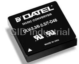
MURATA DLV
Description
Murata DLV Series DC/DC Converter. 30W | Dual Output | Mixed-Voltage
Part Number
DLV
Price
Request Quote
Manufacturer
MURATA
Lead Time
Request Quote
Category
NYC
Features
- 2" x 2" package; Industry standard pinout
- 30 Watts total output power
- Available input voltage ranges: 10-18V, 18-36V or 36-75V
- CE mark available (75VIN models)
- Fully Isolated (1500Vdc)
- IEC950/UL60950/EN60950 certi? ed
- Independent output voltage adjustment
- Input under and overvoltage shutdown
- Output overvoltage protection
- Remote On/Off Control
- Synchronous recti?er; No load operation
- Thermal shutdown
- Two independently regulated outputs: 3.3V @ 6A; 2.5V, 1.8V, 1.5V or 1.2V @ 7A
Datasheet

Extracted Text
® ® INNOVATION and EXC ELLE N C E Dual Output Mixed Voltage, DLV Models VOUT Combinations of 3.3/2.5/1.8/1.5/1.2 Volts 30 Watt, DC/DC Converters PRELIMINARY The DLV (Dual Low Voltage) Series from DATEL provides both digital I/O and Features core logic supply voltages from a single 2" x 2" industry-standard pinout, plastic Two independently regulated outputs: package. The DLV series allows for any dual-output combination of 3.3, 2.5, 1.8, 1.5 3.3V @ 6A; 2.5V, 1.8V, 1.5V or 1.2V @ 7A or 1.2 Volts with associated output currents of 6 Amps for 3.3V outputs and 7 Amps 30 Watts total output power for 1.2-2.5V outputs. Any combination of these output currents is permissable to a Available input voltage ranges: total of 30 Watts of output power. All models are available with input ranges of 10 to 10-18V, 18-36V or 36-75V 18V (-D12), 18 to 36V (-D24) or 36 to 75V (-D48). Plug-in compatibility with a number of converters from other leading manufactur- Independent output voltage adjustment ers is possible because DATEL offers these 30 Watt converters with the ţ exibility to Remote On/Off Control add/remove the higher-voltage trim (pin 5). Each output is independently regulated Synchronous rectiŢ er; No load operation with its own control loop to provide ±1.0% line and load regulation. Fully synchro- 2" x 2" package; Industry standard pinout nous output topology allows no load operation and high efŢ ciencies. Models are available with either positive or negative on/off control. Both outputs are internally IEC950/UL60950/EN60950 certiŢ ed synchronized to eliminate asynchronous beat frequencies. CE mark available (75VIN models) All models include input Pi Ţ ltering, input overvoltage and undervoltage shut- Input under and overvoltage shutdown down circuitry, output overvoltage protection, output short-circuit and current limiting Output overvoltage protection protection and thermal shutdown. These devices meet IEC950, UL60950 and EN60950 safety standards. CB reports are available on request. "-D48" models are Thermal shutdown CE marked (meet LVD requirements). Fully Isolated (1500Vdc) V1 OUTPUT +INPUT SWITCH –INPUT CONTROL OUTPUT RETURN PWM OPTO REFERENCE & INPUT UNDERVOLTAGE CONTROLLER ISOLATION AND OVERVOLTAGE ERROR AMP V1 TRIM COMPARATORS (OPTION) ON/OFF CONTROL V2 TRIM PWM OPTO REFERENCE & SYNC CONTROLLER ISOLATION (OPTION) ERROR AMP V2 OUTPUT SWITCH CONTROL Figure 1. SimpliŢ ed Schematic DATEL, Inc., MansŢ eld, MA 02048 (USA) · Tel: (508)339-3000, (800)233-2765 Fax: (508)339-6356 · Email: sales@datel.com · Internet: www.datel.com 30W, DUAL OUTPUT, MIXED-VOLTAGE DC/DC CONVERT ERS DLV Series ➀ Performance SpeciŢ cations and Ordering Guide Output Input Package R/N (mVp-p) ➂ Regulation (Max.) EfŢ ciency VOUT IOUT ➁ VIN Nom. Range IIN ➄ (Case, Model (Volts) (Amps) Typ. Max. Line Load ➃ (Volts) (Volts) (mA) Min. Typ. Pinout) 2.5 7 75 TBD ±1% ±1% DLV-2.5/7-1.8/7-D12 12 10-18 TBD TBD 83% C26, P48 1.8 7 75 TBD ±1% ±1% 2.5 7 75 TBD ±1% ±1% DLV-2.5/7-1.8/7-D24 24 18-36 TBD TBD 83% C26, P48 1.8 7 75 TBD ±1% ±1% 2.5 7 75 TBD ±1% ±1% DLV-2.5/7-1.8/7-D48 48 36-75 TBD TBD 83% C26, P48 1.8 7 75 TBD ±1% ±1% 3.3 6 75 TBD ±1% ±1% DLV-3.3/6-1.2/7-D12 12 10-18 TBD TBD 83% C26, P54 1.2 7 75 TBD ±1% ±1% 3.3 6 75 TBD ±1% ±1% DLV-3.3/6-1.2/7-D24 24 18-36 TBD TBD 83% C26, P54 1.2 7 75 TBD ±1% ±1% 3.3 6 75 TBD ±1% ±1% DLV-3.3/6-1.2/7-D48 48 36-75 TBD TBD 83% C26, P54 1.2 7 75 TBD ±1% ±1% 3.3 6 75 TBD ±1% ±1% DLV-3.3/6-1.5/7-D12 12 10-18 TBD TBD 85% C26, P54 1.5 7 75 TBD ±1% ±1% 3.3 6 75 TBD ±1% ±1% DLV-3.3/6-1.5/7-D24 24 18-36 TBD TBD 85% C26, P54 1.5 7 75 TBD ±1% ±1% 3.3 6 75 TBD ±1% ±1% DLV-3.3/6-1.5/7-D48 48 36-75 TBD TBD 85% C26, P54 1.5 7 75 TBD ±1% ±1% 3.3 6 75 TBD ±1% ±1% DLV-3.3/6-1.8/7-D12 12 10-18 TBD TBD 83% C26, P47 1.8 7 75 TBD ±1% ±1% 3.3 6 75 TBD ±1% ±1% DLV-3.3/6-1.8/7-D24 24 18-36 TBD TBD 83% C26, P47 1.8 7 75 TBD ±1% ±1% 3.3 6 75 TBD ±1% ±1% DLV-3.3/6-1.8/7-D48 48 36-75 TBD TBD 83% C26, P47 1.8 7 75 TBD ±1% ±1% 3.3 6 75 TBD ±1% ±1% DLV-3.3/6-2.5/7-D12 12 10-18 TBD TBD 85% C26, P40 2.5 7 75 TBD ±1% ±1% 3.3 6 75 TBD ±1% ±1% DLV-3.3/6-2.5/7-D24 24 18-36 TBD TBD 85% C26, P40 2.5 7 75 TBD ±1% ±1% 3.3 6 75 TBD ±1% ±1% DLV-3.3/6-2.5/7-D48 48 36-75 TBD TBD 85% C26, P40 2.5 7 75 TBD ±1% ±1% ➀ Typical at TA = +25°C under nominal line voltage and "balanced," full-power conditions: ➂ Ripple/Noise (R/N) measured over a 20MHz bandwidth. All models are specicfi ed with TBD ceramic capacitors. 3.3V @ 4.5A/2.5V @ 6A; 3.3V @ 5.2A/1.8V @ 7A; 3.3V @ 5.2A/1.8V @ 7A; 2.5V @ 7A/1.8V @ 7A. ➃ Tested from no load to 100% load (other output at no load).➁ Any combination of rated IOUT current, not to exceed 30 Watts of output power. (See derating graphs.)➄ Nominal line voltage, no load/balanced full-power condition. MECHANICAL SPECIFICATIONS See page 5 for Part Number Structure and ordering details. 2.00 DLV-/ 3.3 6 - 2.5/- 7 D48 T N (50.08) Dual Low Voltage/ Add T and N suffi xes as desired PLASTIC CASE Mixed-Voltage Series 0.48 Input Voltage Range: Case C26 (12.19) V1 Nominal Output Voltage D12 = 10-18 Volts (12V nominal) D24 = 18-36 Volts (24V nominal) I1 Maximum Output Current D48 = 36-75 Volts (48V nominal) STANDOFF V2 Nominal Output Voltage 0.040 ±0.001 DIA. I2 Maximum Output Current 0.020 (0.51) (1.016 ±0.025) 0.20 MIN 1.800 0.10 (5.08) (45.72) (2.54) I/O Connections Pin Function P40 Function P47 Function P48 Function P54 5 1 +Input +Input +Input +Input 6 0.200 2 –Input –Input –Input –Input (5.08) 3 No Pin No Pin No Pin No Pin 1.400 7 1.200 4 On/Off Control On/Off Control On/Off Control On/Off Control (35.56) 1 (30.48) 2.00 5 +3.3V Trim* +3.3V Trim* +2.5V Trim* +3.3V Trim* 3 EQ. SP. @ 2 (50.08) 0.10 0.400 (10.16) 8 6 +3.3V Output +3.3V Output +2.5V Output +3.3V Output 0.400 (2.54) (10.16) 7 Output Return Output Return Output Return Output Return 4 9 8 +2.5V Output +1.8V Output +1.8V Output +1.5V Output 9 +2.5V Trim +1.8V Trim +1.8V Trim +1.5V Trim 0.40 (10.16) * Optional pins BOTTOM VIEW DIMENSIONS ARE IN INCHES (MM) 2 PRELIMINARY 30W, DUAL OUTPUT, MIXED-VO LTAGE DC/DC CONVERT ERS DLV Models Performance/Functional SpeciŢ cations Output (continued) Typical @ TA = +25°C under nominal line voltage, balanced "full-load" conditions, unless noted. ➀ Current Limit Inception: 3.3/1.8V Models Input 3.3V @ 98.5%VOUT, 1.8V @ TBDA TBD Amps Input Voltage Range: 1.8V @ 98%VOUT, 3.3V @ TBDA TBD Amps 98.5%VOUT D12 Models 10-18 Volts (12V nominal) 3.3V/2.5V Models D24 Models 18-36 Volts (24V nominal) 3.3V @ 98.5%VOUT, , 2.5V @ TBDA TBD Amps D48 Models 36-75 Volts (48V nominal) 2.5V @ 98%VOUT, 3.3V @ TBDA TBD Amps Overvoltage Shutdown: Short Circuit Current: D12 Models 19-23 Volts (21V nominal) 3.3V Outputs TBD Amps average, continuous D24 Models 37-42 Volts (40V nominal) 2.5V Outputs TBD Amps average, continuous D48 Models 77-81 Volts (79V nominal) 1.8V Outputs TBD Amps average, continuous Start-Up Threshold: 1.5V Outputs TBD Amps average, continuous D12 Models 9-10 Volts (9.3V nominal) Overvoltage Protection: Comparator, magnetic feedback D24 Models 16.5-18 Volts (17V nominal) 2.5/1.8V Models TBD/TBD D48 Models 34.5-36 Volts (35V nominal) 3.3/1.5V Models TBD/TBD Undervoltage Shutdown: 3.3/1.8V Models TBD/TBD D12 Models 8.5-9.6 Volts (9.3V nominal) 3.3/2.5V Models TBD/TBD D24 Models 16-17 Volts (16.5V nominal) Maximum Capacitive Loading D48 Models 33-35 Volts (34V nominal) 2.5/1.8V Models TBD/TBDµF Input Current: 3.3/1.5V Models TBD/TBDµF Normal Operating Conditions See Ordering Guide 3.3/1.8V Models TBD/TBDµF Standby Mode: 3.3/2.5V Models TBD/TBDµF Off, OV, UV, Thermal Shutdown 10mA typical Temperature CoefŢ cient ±0.02% per °C Input Reţ ected Ripple Current: Dynamic Characteristics Source Impedance Dynamic Load Response: D12 Models TBD 2.5/1.8V Models D24 Models TBD 2.5V (50-100% step to 1.5%VOUT) TBD µsec maximum D48 Models TBD 1.8V (50-100% step to 2%VOUT) TBD µsec maximum Internal Input Filter Type Pi (0.039µF - 2.2µH - TBD) 3.3/1.5V Models Reverse-Polarity Protection: 3.3V (50-100% step to 1%VOUT) TBD µsec maximum D12 Models TBD minute duration, 6A maximum 1.8V (50-100% step to 2%VOUT) TBD µsec maximum D24 Models TBD minute duration, 4A maximum 3.3/1.8V Models D48 Models TBD minute duration, 2A maximum 3.3V (50-100% step to 1%VOUT) TBD µsec maximum 1.8V (50-100% step to 2%VOUT) TBD µsec maximum On/Off Control (Pin 4): ➂ ➃ ➅ 3.3V/2.5V Models D12, D24, D48 Models On = open or TBD to +VIN, 3.3V (50-100% step to 1%VOUT) TBD µsec maximum IIN = TBDµA @ TBDV 2.5V (50-100% step to 1.5%VOUT) TBD µsec maximum Off = 0-0.8V, IIN = TBD @ 0V D12N, D24N, D48N Models On = 0-0.8V, IIN = TBD @ 0V Start-Up Time: Off = open or TBD to +5.5V VIN to VOUT TBD IIN = TBDµA @ TBDV On/Off to VOUT TBD Output Switching Frequency 225kHz (±TBD kHz) VOUT Accuracy Environmental 2.5V/1.8V Models 1.5% / 2% maximum MTBF 3.3V/1.5V and 3.3V/1.8VModels 1% / 2% maximum D12 Models TBD hours 3.3V/2.5V Models 1% / 1.5% maximum D24 Models TBD hours Minimum Loading Per SpeciŢ cation No load D48 Models TBD hours Ripple/Noise (20MHz BW) See Ordering Guide Operating Temperature (Ambient): Without Derating: Line/Load Regulation See Ordering Guide 2.5/1.8V Models TBD EfŢ ciency See Ordering Guide/Effi ciency Curves 3.3/1.8V Models TBD Trim Range ➇ ±5% each output 3.3V/2.5V Models TBD Isolation Voltage: With Derating To +100°C (See Derating Curves) Input-to-Output 1500Vdc Case Temperature: Maximum Operational +100°C Isolation Capacitance 470pF For Thermal Shutdown TBD minimum, TBD maximum Isolation Resistance 100MΩ Storage Temperature –40 to +120°C Current Limit Inception: 2.5/1.8V Models 2.5V @ 98%VOUT, 1.8V @ TBDA TBD Amps 1.8V @ 98%VOUT, 2.5V @ TBDA TBD Amps 3.3/1.5V Models 3.3V @ 98.5%VOUT, 1.5V @ TBDA TBD Amps 1.5V @ 98%VOUT, 3.3V @ TBDA TBD Amps 3 30W, DUAL OUTPUT, MIXED-VOLTAGE DC/DC CONVERT ERS DLV Series Trimming Output Voltages Physical Dimensions 2" x 2" x 0.5" (50.8 x 50.8 x 12.7mm) These DLV converters have a trim capability (pins 9 & 5) that allow users Case Material Diallyl phthalate, UL94V-0 rated to independently adjust the output voltages ±5%. (Note: pin 5 is an option, Pin Material Brass, solder coated see ordering information.) Adjustments to the output voltages can be accom- plished via a trim pot, Figure 2, or a single fi xed resistor as shown in Figures Weight: TBD 3 and 4. A single fi xed resistor can increase or decrease the output voltage Primary to Secondary Insulation Level Operational depending on its connection. Fixed resistors should have absolute TCR's less ➀ All models are specifi ed with external TBD ceramic output capacitors. than 100ppm/°C to minimize sensitivity to changes in temperature. ➁ See Technical Notes/Graphs for details. ➂ Devices may be order with opposite polarity. See Part Number Suffi xes and Technical Notes A single resistor connected from the Trim pin 9 to +Output (pin 8), see Figure for details. 3, will decrease the lower output voltage. A resistor connected from Trim pin 9 ➃ Applying a voltage to On/Off Control (pin 4) when no input power is applied to the converter to Output Return (pin 7) will increase the lower output voltage. See Figure 4. may cause permanent damage. ➄ Output noise may be further reduced with the installation of additional external output Similarly, the higher output voltage can be adjusted using a single resistor capacitors. See Technical Notes. ➅ On/Off control is designed to be driven with open collector or by appropriate voltage connected from the Trim (pin 5) to +Output (pin 6) or to Output Return (pin levels. Voltages must be referenced to the –Input (pin 2). 7). See Figures 3 and 4. ➆ Demonstrated MTBF available on request. ➇ Trim function for the higher of two voltages available with "T" suffi x. See Part Number Suffi xes and Technical Notes for details. 5 +3.3V TRIM * 1 Absolute Maximum Ratings +INPUT 6 +3.3V OUTPUT Input Voltage: 20kΩ +3.3V 5-22 2 Continuous: D12 Models 23 Volts –INPUT LOAD TURNS D2A Models 42 Volts 7 OUTPUT RETURN D48 Models 81 Volts 3 20kΩ +2.5V Transient (100msec): D12 Models 25 Volts SYNC * 5-22 LOAD TURNS D24 Models 50 Volts 8 D48 Models 100 Volts +2.5V OUTPUT 4 ON/OFF CONTROL 9 Input Reverse-Polarity Protection ➁ Input Current must be limited. TBD +2.5V TRIM minute duration. Fusing recommended. * OPTIONAL PIN D12A Models 6 Amps D24A Models 4 Amps Figure 2. Trim Connections Using A Trim Pot D48A Models 2 Amps Output Current ➁ Current limited. Devices can withstand an indefi nite output short circuit. RTRIM DOWN 5 +3.3V TRIM * On/Off Control (Pin 4) Max. Voltages 1 +INPUT 6 Referenced to –Input (pin 2) +3.3V OUTPUT No Suffi x +VIN +3.3V 2 "N" Suffi x +8 Volts –INPUT LOAD OUTPUT 7 Sync Control (Pin 3) Max. Voltages RETURN "S" Suffi x +5.7 Volts 3 +2.5V SYNC * LOAD Storage Temperature –40 to +120°C 8 +2.5V OUTPUT 4 Lead Temperature (Soldering, 10 sec.) +300°C ON/OFF CONTROL 9 These are stress ratings. Exposure of devices to any of these conditions may adversely +2.5V TRIM RTRIM DOWN affect long-term reliability. Proper operation under conditions other than those listed in the * OPTIONAL PIN Performance/Functional Specifi cations Table is not implied, nor recommended. Figure 3. Trim Connections To Decrease Output Voltages Using Fixed Resistors TECHNICAL NOTES 3.3 Volt Trim Down L 3.48(VO – 1.577) On/Off Control RT (kΩ) = –28.7 DOWN 3.3 – VO N The primary-side, remote On/Off Control function (pin 4) can be specifi ed to operate with either positive or negative polarity. Positive polarity devices (no 2.5 Volt Trim Down suffi x) are enabled when pin 4 is left open or pulled high (+TBDV to +TBDV L 2.41(VO – 1.18) RT (kΩ) = –19.7 DOWN with respect to –Input). Positive polarity devices are disabled when pin 4 is 2.5 – VO N pulled low (0-0.8V with respect to –Input). Negative polarity devices are off when pin 4 is high/open and on when pin 2 is pulled low. 1.8 Volt Trim Down L 1.73(VO – 0.86) For applications where power sequencing is critical, the DLV series can be RT (kΩ) = –14.17 DOWN 1.8 – VO confi gured such that the On/Off Control pin will enable/disable only the higher N of the two output voltages. Contact DATEL for more information. 4 L N L N L N 30W, DUAL OUTPUT, MIXED-VO LTAGE DC/DC CONVERT ERS DLV Models RTRIM UP 3.3 Volt Trim Up 5 +3.3V TRIM * L 2.84 1 +INPUT 6 RT (kΩ) = –19.7 UP +3.3V OUTPUT VO – 2.5 N +3.3V 2 Note: Resistor values are in kΩ. Accuracy –INPUT LOAD 2.5 Volt Trim Up OUTPUT 7 of adjustment is subject to L RETURN 5.88 3 RT (kΩ) = –28.7 tolerances of resistors and fac- UP +2.5V SYNC * VO – 3.3 N LOAD tory-adjusted output accuracy. 8 +2.5V OUTPUT VO = desired output voltage. 4 ON/OFF 1.8 Volt Trim Up CONTROL 9 +2.5V TRIM L 1.49 RTRIM UP RT (kΩ) = –14.17 * OPTIONAL PIN UP VO – 1.8 N Figure 4. Trim Connections To Increase Output Voltages Using Fixed Resistors PA RT NUMBER STRUCTURE Part Number SufŢ xes Standard DLV DC/DC’s provide a Trim function (Pin 9) for the lower DLV-/ 3.3 6 - 2.5/- 7 D48 T N of the two output voltages. A Trim pin (Pin 5) for the higher voltage can be added by indicating a "T" suffi x. An "N" suffi x indicates that the On/Off Dual Low Voltage/ Add T and N suffi xes Control function incorporates negative polarity logic. Mixed-Voltage Series as desired No SufŢ x Pins 5 not installed, positive polarity On/Off Control Input Voltage Range: V1 Nominal Output Voltage T SufŢ x Pin 5 added for higher voltage Trim option D12 = 10-18 Volts (12V nominal) N SufŢ x Negative polarity On/Off Control I1 Maximum Output Current D24 = 18-36 Volts (24V nominal) D48 = 36-75 Volts (48V nominal) V2 Nominal Output Voltage I2 Maximum Output Current ® ® INNOVATION and EXC ELLE N C E ISO 9001 REGISTERED DS-0490 6/01 DATEL (UK) LTD. Tadley, England Tel: (01256)-880444 DATEL, Inc. 11 Cabot Boulevard, Mansfi eld, MA 02048-1151 DATEL S.A.R.L. Montigny Le Bretonneux, France Tel: 01-34-60-01-01 Tel: (508) 339-3000 (800) 233-2765 Fax: (508) 339-6356 DATEL GmbH München, Germany Tel: 89-544334-0 Internet: www.datel.com Email: sales@datel.com DATEL KK Tokyo, Japan Tel: 3-3779-1031, Osaka Tel: 6-6354-2025 DATEL makes no representation that the use of its products in the circuits described herein, or the use of other technical information contained herein, will not infringe upon existing or future patent rights. The descriptions contained herein do not imply the granting of licenses to make, use, or sell equipment constructed in accordance therewith. Specifi cations are subject to change without notice. The DATEL logo is a registered DATEL, Inc. trademark. 5 L N L N L N
Frequently asked questions
What makes Elite.Parts unique?

What kind of warranty will the DLV have?
Which carriers does Elite.Parts work with?
Will Elite.Parts sell to me even though I live outside the USA?
I have a preferred payment method. Will Elite.Parts accept it?


What they say about us
FANTASTIC RESOURCE
One of our top priorities is maintaining our business with precision, and we are constantly looking for affiliates that can help us achieve our goal. With the aid of GID Industrial, our obsolete product management has never been more efficient. They have been a great resource to our company, and have quickly become a go-to supplier on our list!
Bucher Emhart Glass
EXCELLENT SERVICE
With our strict fundamentals and high expectations, we were surprised when we came across GID Industrial and their competitive pricing. When we approached them with our issue, they were incredibly confident in being able to provide us with a seamless solution at the best price for us. GID Industrial quickly understood our needs and provided us with excellent service, as well as fully tested product to ensure what we received would be the right fit for our company.
Fuji
HARD TO FIND A BETTER PROVIDER
Our company provides services to aid in the manufacture of technological products, such as semiconductors and flat panel displays, and often searching for distributors of obsolete product we require can waste time and money. Finding GID Industrial proved to be a great asset to our company, with cost effective solutions and superior knowledge on all of their materials, it’d be hard to find a better provider of obsolete or hard to find products.
Applied Materials
CONSISTENTLY DELIVERS QUALITY SOLUTIONS
Over the years, the equipment used in our company becomes discontinued, but they’re still of great use to us and our customers. Once these products are no longer available through the manufacturer, finding a reliable, quick supplier is a necessity, and luckily for us, GID Industrial has provided the most trustworthy, quality solutions to our obsolete component needs.
Nidec Vamco
TERRIFIC RESOURCE
This company has been a terrific help to us (I work for Trican Well Service) in sourcing the Micron Ram Memory we needed for our Siemens computers. Great service! And great pricing! I know when the product is shipping and when it will arrive, all the way through the ordering process.
Trican Well Service
GO TO SOURCE
When I can't find an obsolete part, I first call GID and they'll come up with my parts every time. Great customer service and follow up as well. Scott emails me from time to time to touch base and see if we're having trouble finding something.....which is often with our 25 yr old equipment.
ConAgra Foods