www.DataSheet.co.kr
LM201U04
Liquid Crystal Display
Product Specification
SPECIFICATION
FOR
APPROVAL
( ) Preliminary Specification
( ◆ ) Final Specification
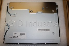
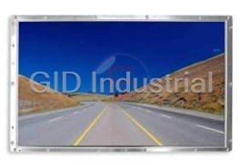
Title 20.1” UXGA TFT LCD
BUYER SUPPLIER LG.Philips LCD CO., Ltd.
MODEL *MODEL LM201U04
SUFFIX SL02
*When you obtain standard approval,
please use the above model name without suffix
SIGNATURE DATE
APPROVED BY DATE
S.G. Hong / G. Manager
/
REVIEWED BY
K. G. Park / Manager
/
PREPARED BY
D.I.Chung / A . Engineer
/
Please return 1 copy for your confirmation with Product Engineering Dept.
your signature and comments. LG. Philips LCD Co., Ltd
1/27
Ver 1.0 May. 27. 2005
Datasheet pdf - http://www.DataSheet4U.net/
www.DataSheet.co.kr
LM201U04
Liquid Crystal Display
Product Specification
CONTENTS
NO. ITEM Page
- COVER 1
- CONTENTS 2
- RECORD OF REVISIONS 3
1 GENERAL DESCRIPTION 4
2 ABSOLUTE MAXIMUM RATINGS 5
3 ELECTRICAL SPECIFICATIONS 6
3-1 ELECTRICAL CHARACTERISTICS 6
3-2 INTERFACE CONNECTIONS 8
3-3 SIGNAL TIMING SPECIFICATIONS 10
3-4 SIGNAL TIMING WAVE FORMS 11
3-5 COLOR INPUT DATA REFERENCE 12
3-6 POWER SEQUENCE 13
4 OPTICAL SPECIFICATIONS 14
5 MECHANICAL CHARACTERISTICS 19
6 RELIABILITY 22
7 INTERNATIONAL STANDARDS 23
7-1 SAFETY 23
7-2 EMC 23
8 PACKING 24
8-1 DESIGNATION OF LOT MARK 24
8-2 PACKING FORM 24
9 PRECAUTIONS 25
10 OTHERS -
APPENDIX 1. REQUIRED SIGNAL ASSIGNMENT FOR FLATLink Transmitter 27
2/27
Ver 1.0 May. 27. 2005
Datasheet pdf - http://www.DataSheet4U.net/
www.DataSheet.co.kr
LM201U04
Liquid Crystal Display
Product Specification
RECORD OF REVISIONS
Revision No Date Page Description
0.0 Jan. 12. 2005 First Draft, Preliminary Specifications
6
0.1 Mar. 22. 2005 Update Power Consumption at Mosaic pattern
10
Change Timing specification on page 10
6
0.2 May. 16. 2005 Change Type Power Consumption at Mosaic Pattern
21
Change Wire Length from 120mm → 89mm at Rear View
14
1.0 May. 27. 2005 Change Luminance uniformity specification :
Max 1.33 → Max 1.39
Final Draft.
3/27
Ver 1.0 May. 27. 2005
Datasheet pdf - http://www.DataSheet4U.net/
Gate Driver Circuit
www.DataSheet.co.kr
LM201U04
Liquid Crystal Display
Product Specification
1. General Description
The LM201U04-SL02is a Color Active Matrix Liquid Crystal Display with an integral Cold Cathode Fluorescent
Lamp(CCFL) backlight system. The matrix employs a-Si Thin Film Transistor as the active element.
It is a transmissive type display operating in the normally black mode. This TFT-LCD has a 20.1 inch diagonally
measured active display area with UXGA resolution(1200 vertical by 1600 horizontal pixel array).
Each pixel is divided into Red, Green and Blue sub-pixels or dots which are arranged in vertical stripes.
Gray scale or the brightness of the sub-pixel color is determined with a 8-bit gray scale signal for each dot,
thus, presenting a palette of more than 16,777,216 colors.
The LM201U04-SL02 has been designed to apply the interface method that enables low power, high speed,low
EMI. FPD Link must be used as a LVDS(Low Voltage Differential Signaling) chip.
The LM201U04-SL02 is intended to support applications where thin thickness, wide viewing angle, low power are
critical factors and graphic displays are important. In combination with the vertical arrangement of the sub-pixels,
the LM201U04-SL02 characteristics provide an excellent flat panel display for office automation products such as
monitors.
G1
LVDS
pair #1
Timing Controller
CN1
(30pin)
&LVDS 1 Chip
TFT - LCD Panel
LVDS
pair #2 (1600 × RGB × 1200 pixels)
G1200
S1 S1600
RGB
+20V
Power Circuit
Vcc
Block Source Driver Circuit
CN1(4pin),CN2(2pin))
Back light Assembly (6CCFL)
CN3(2pin),CN4(4pin)
General Features
Active screen size 20.1 inches (510.54mm) diagonal
Outline Dimension 432.0(H) x 331.5(V) x 25.0(D) mm(Typ.)
Pixel Pitch 0.255 mm x 0.255 mm
Pixel Format 1600 horizontal By 1200 vertical Pixels RGB stripe arrangement
Color depth 8-bits, 16,777,216 colors
2
Luminance, white 300 cd/m (Typ. Center 1 point)
Power Consumption Total 34.98 Watt(Typ.), (5.58 Watt @Vcc, 29.4 Watt @300cd/㎡ [Lamp=7.0mA])
Weight 3200g (Typ.)
Display operating mode Transmissive mode, normally black
Surface treatments Hard coating (3H), Anti-glare treatment of the front polarizer
4/27
Ver 1.0 May. 27. 2005
Datasheet pdf - http://www.DataSheet4U.net/
www.DataSheet.co.kr
LM201U04
Liquid Crystal Display
Product Specification
2. Absolute Maximum Ratings
The following are maximum values which, if exceeded, may cause faulty operation or damage to the unit.
Table 1. ABSOLUTE MAXIMUM RATINGS
Values
Parameter Symbol Units Notes
Min. Max.
Power Input Voltage V -0.3 +23 V at 25℃
CC dc
Operating Temperature T 0 +50 ℃ 1
OP
Storage Temperature T -20 +60 ℃ 1
ST
Operating Ambient Humidity H 10 +90 %RH 1
OP
Storage Humidity H 5 +90 %RH 1
ST
Note : 1. Temperature and relative humidity range are shown in the figure below.
Wet bulb temperature should be 39 °C Max, and no condensation of water.
5/27
Ver 1.0 May. 27. 2005
Datasheet pdf - http://www.DataSheet4U.net/
www.DataSheet.co.kr
LM201U04
Liquid Crystal Display
Product Specification
3. Electrical Specifications
3-1. Electrical Characteristics
The LM201U04-SL02 requires two power inputs. One is employed to power the LCD electronics and to
drive the TFT array and liquid crystal. The second input which powers the CCFL, is typically generated
by an inverter. The inverter is an external unit to the LCD.
Table 2. ELECTRICAL CHARACTERISTICS
Values
Parameter Symbol
Units Notes
Min. Typ. Max.
MODULE:
Vdc
Power Supply Input Voltage V
18V 20V 22V
CC
A 1
Power Supply Input Current I
0.28 0.36
CC
W 1
Power Consumption P
5.58 7.20
c
Ohm 2
Differential Impedance Zm
100
A 3
Rush Current I
3
Rush
LAMP (each CCFL)
V 4
Operating voltage V
680(7.5mA) 700 825(3mA)
RMS
BL
mA
Operating Current I
3.0 7.0 7.5
BL
5
Established Starting Voltage Vs
V
at 25℃
- - 1150
RMS
V
at 0℃
- - 1450
RMS
KHz 6
Operating Frequency F
40 50 80
BL
Watts 7
Power Consumption (6 CCFL’s) P
- 29.4 32.3
BL
Minutes 8
Discharge Stabilization Time Ts
- - 3
Hours 9
Life time
45000 - -
Notes :1. The specified current and power consumption are under the V =20.0V, 25°C, f =60Hz condition,
CC V
Typical supply current is measured at the condition of 8 X 6 chess pattern(white & black)
2. This impedance value is for impedance matching between LVDS T and
X
the mating connector of the LCD.
3. The duration of rush current is about 1ms.
4. Operating voltage is measured at 25°C. The variance of the voltage is ±10%.
5. The output voltage at the transformer in the inverter must be high considering to the loss of the
ballast capacitor in the inverter. The voltage above V should be applied to the lamps for more
S
than 1 second for start-up. Otherwise, the lamps may not be turned on.
6. Lamp frequency may produce interface with horizontal synchronous frequency and as a result this
may cause beat on the display. Therefore lamp frequency shall be as away possible from the
horizontal synchronous frequency and from its harmonics in order to prevent interference.
7. The lamp power consumption shown above does not include loss of external inverter at 25°C.
The used lamp current is the lamp typical current.
8. Let’s define the brightness of the lamp after being lighted for 5 minutes as 100%.
T is the time required for the brightness of the center of the lamp to be not less than 95%.
S
The used lamp current is the lamp typical current.
9. The life time is defined as the time at which brightness of lamp is 50% compare to that of initial
value at the typical lamp current on condition of continuous operating at 25±2°C.
6/27
Ver 1.0 May. 27. 2005
Datasheet pdf - http://www.DataSheet4U.net/
www.DataSheet.co.kr
LM201U04
Liquid Crystal Display
Product Specification
Note. Do not attach a conducting tape to connecting wire.
If the lamp wire attach to a conducting tape, TFT-LCD Module has a low luminance and the
inverter has abnormal action. Because leakage current is occurred between lamp wire and
conducting tape.
The design of the inverter must have specifications for the lamp in LCD Assembly.
The performance of the Lamp in LCM, for example life time or brightness, is extremely influenced by
the characteristics of the DC-AC inverter. So all the parameters of an inverter should be carefully
designed so as not to produce too much leakage current from high-voltage output of the inverter.
When you design or order the inverter, please make sure unwanted lighting caused by the mismatch
of the lamp and the inverter(no lighting, flicker, etc) never occurs. When you confirm it, the LCD –
Assembly should be operated in the same condition as installed in you instrument.
Requirements for a system inverter design, which is intended to have a better display performance, a
better power efficiency and a more reliable lamp.
It shall help increase the lamp lifetime and reduce its leakage current.
a. The asymmetry rate of the inverter current and voltage waveform should be 10% below;
b. The distortion rate of the current and voltage waveform should be within √2 ±10%;
c. The ideal sine current and voltage waveform shall be symmetric in positive and negative polarities.
* Asymmetry rate = | I –I | / I * 100%
p –p rms
I p
* Distortion rate = I (or I ) / I
I -p p –p rms
7/27
Ver 1.0 May. 27. 2005
Datasheet pdf - http://www.DataSheet4U.net/
www.DataSheet.co.kr
LM201U04
Liquid Crystal Display
Product Specification
3-2. Interface Connections
Interface chip must be used LVDS, part No. DS90CF383MTD(Transmitter) made by National Semiconductor.
Or used the compatible interface chips(TI:SN75LVDS83).
This LCD employs seven interface connections, a 30-pin connector is used for the module electronics interface.
Six 2-pin connectors are used for the integral back-light system.
The electronics interface connector is a model FI-XB30SRL-HF11 manufactured by JAE or used the connector
MDF76RAW-30S-1H manufactured by HIROSE
The mating connector part number FI-X30M(JAE) or equivalent.
The pin configuration for the connector is shown in the table 3.
Table 3. MODULE CONNECTOR PIN CONFIGURATION(LVDS)
Pin Symbol Description
Vcc
1 Supply voltage for LCD module
Vcc
2 Supply voltage for LCD module
Vcc
3 Supply voltage for LCD module
Vcc
4 Supply voltage for LCD module
GND
5 Ground
GND
6 Ground
SR3P
7 Plus signal of even channel 3 (LVDS)
SR3M
8 Minus signal of even channel 3 (LVDS)
SCLKINP
9 Plus signal of even clock channel (LVDS)
SCLKINM
10 Minus signal of even clock channel (LVDS)
SR2P
11 Plus signal of even channel 2 (LVDS)
Second data
12 SR2M
Minus signal of even channel 2 (LVDS)
13 SR1P
Plus signal of even channel 1 (LVDS)
14 SR1M
Minus signal of even channel 1 (LVDS)
15 SR0P
Plus signal of even channel 0 (LVDS)
16 SR0M
Minus signal of even channel 0 (LVDS)
17 GND
Ground
18 GND
Ground
19 FR3P
Plus signal of odd channel 3 (LVDS)
20 FR3M
Minus signal of odd channel 3 (LVDS)
21 FCLKINP
Plus signal of odd clock channel (LVDS)
22 FCLKINM
Minus signal of odd clock channel (LVDS)
23 FR2P
Plus signal of odd channel 2 (LVDS)
First data
24 FR2M
Minus signal of odd channel 2 (LVDS)
25 FR1P
Plus signal of odd channel 1 (LVDS)
26 FR1M
Minus signal of odd channel 1 (LVDS)
27 FR0P
Plus signal of odd channel 0 (LVDS)
28 FR0M
Minus signal of odd channel 0 (LVDS)
29 GND
Ground
30 GND
Ground
Connector pin arrangement
30 1
P/N, Maker :
FI-XB30SRL-HF11, JAE
8/27
Ver 1.0 May. 27. 2005
Datasheet pdf - http://www.DataSheet4U.net/
www.DataSheet.co.kr
LM201U04
Liquid Crystal Display
Product Specification
The backlight interface connector is a model BHSR-02VS-1(CN2/CN3) and BHR-05VS-1 (CN1/CN4)
manufactured by JST. The mating connector part number are SM02B-BHSS-1-TB(2pin), SM04(9-E2)B-
BHS-1-TB or equivalent. The pin configuration for the connector is shown in the table below.
Table 4. BACKLIGHT CONNECTOR PIN CONFIGURATION
No Pin Symbol Description Notes
1 HV Power supply for lamp 1(High voltage side) 1
CN1
2 HV Power supply for lamp 2(High voltage side) 1
3 NC NC
4 LV Power supply for lamp 1(Low voltage side)
5 LV Power supply for lamp 2(Low voltage side)
1 HV Power supply for lamp 3(High voltage side) 1
CN2
2 LV Power supply for lamp 3(Low voltage side)
1 HV Power supply for lamp 4(High voltage side) 1
CN3
2 LV Power supply for lamp 4(Low voltage side)
1 HV Power supply for lamp 6(High voltage side) 1
CN4
2 HV Power supply for lamp 5(High voltage side) 1
3 NC NC
4 LV Power supply for lamp 6(Low voltage side)
5 LV Power supply for lamp 5Low voltage side)
Notes: 1. The high voltage power terminal is thick line.
2. The low voltage power terminal is thin line.
Up Side
Lamp1
CN 1
Lamp 2
Lamp 3
CN 2
Down Side
Lamp 4
CN 3
Lamp 5
CN 4
Lamp 6
9/27
Ver 1.0 May. 27. 2005
Datasheet pdf - http://www.DataSheet4U.net/
www.DataSheet.co.kr
LM201U04
Liquid Crystal Display
Product Specification
3-3. Signal Timing Specifications
This is the signal timing required at the input of the LVDS Transmitter. All of the interface signal timing
should be satisfied with the following specifications for it’s proper operation.
Table 5. Timing Table
ITEM SYMBOL Min Typ Max Unit Note
tCLK
Period 14.28 16.00 16.26 ns
DCLK
fCLK
MHz 2pixels/clk
Frequency 61.5 62.5 70.0
tHP
Hsync Period 832 840 906 1
tCLK
tWH
2
Width-Active 16 16 16
tVP
tHP
Vsync Period 1230 1240 1250
fV
Frequency 59 60 61 Hz 3
tWV
tHP 4
Width-Active 3 3 3
tHV
Data Horizontal Valid 800 800 800
Enable
tHBP
Horizontal Back Porch 8 16 16
tCLK
tHFP
Horizontal Front Porch 8 8 36
-
Horizontal Blank 32 40 68 tWH+ tHBP+ tHFP
tVV
Vertical Valid 1200 1200 1200
tVBP
Vertical Back Porch 25 35 35
tHP
tVFP
Vertical Front Porch 2 2 2
-
tWV+ tVBP+ tVFP
Vertical Blank 30 40 50
Notes: 1. Hsync period shall be a double number of 4 (based on 2pixels/clk)
2. Horizontal sync shall be active high.
3. Vertical frequency should be keep the above specification when the resolution & mode are changed.
4. Vertical sync shall be active high.
10 /27
Ver 1.0 May. 27. 2005
Datasheet pdf - http://www.DataSheet4U.net/
www.DataSheet.co.kr
LM201U04
Liquid Crystal Display
Product Specification
3-4. Signal Timing Waveforms
0.7Vcc
Hsync, Vsync, DE, DATA
0.3Vcc
t
CLK
0.5V
CC
Dclk
VALID
INVALID
INVALID
DATA
DE(Data Enable)
Data are latched at the falling edge of DCLK
t
HP
t
Hsync
WH
t t
t
HBP HV
HFP
DE(Data Enable)
t
VP
t
WV
Vsync
t
t t
VFP
VBP VV
DE(Data Enable)
11 /27
Ver 1.0 May. 27. 2005
Datasheet pdf - http://www.DataSheet4U.net/
www.DataSheet.co.kr
LM201U04
Liquid Crystal Display
Product Specification
3-5. Color Input Data Reference
The brightness of each primary color(red,green and blue) is based on the 8-bit gray scale data input for the
color ; the higher the binary input, the brighter the color. The table below provides a reference for color
versus data input.
Table 6. COLOR DATA REFERENCE
Input Color Data
Red Green Blue
Color
MSB LSB MSB LSB MSB LSB
R7 R6 R5 R4 R3 R2 R1 R0 G7 G6 G5 G4 G3 G2 G1 G0 B7 B6 B5 B4 B3 B2 B1 B0
Black 0 0 0 0 0 0 0 0 0 0 0 0 0 0 0 0 0 0 0 0 0 0 0 0
Red (255) 1 1 1 1 1 1 1 1 0 0 0 0 0 0 0 0 0 0 0 0 0 0 0 0
Green (255) 0 0 0 0 0 0 0 0 1 1 1 1 1 1 1 1 0 0 0 0 0 0 0 0
Blue (255)
Basic 0 0 0 0 0 0 0 0 0 0 0 0 0 0 0 0 1 1 1 1 1 1 1 1
Cyan
Color 0 0 0 0 0 0 0 0 1 1 1 1 1 1 1 1 1 1 1 1 1 1 1 1
Magenta 1 1 1 1 1 1 1 1 0 0 0 0 0 0 0 0 1 1 1 1 1 1 1 1
Yellow
1 1 1 1 1 1 1 1 1 1 1 1 1 1 1 1 0 0 0 0 0 0 0 0
White
1 1 1 1 1 1 1 1 1 1 1 1 1 1 1 1 1 1 1 1 1 1 1 1
Red(000) Dark 0 0 0 0 0 0 0 0 0 0 0 0 0 0 0 0 0 0 0 0 0 0 0 0
Red(001) 0 0 0 0 0 0 0 1 0 0 0 0 0 0 0 0 0 0 0 0 0 0 0 0
Red(002) 0 0 0 0 0 0 1 0 0 0 0 0 0 0 0 0 0 0 0 0 0 0 0 0
--- ------
- - - - - - - - - - - - - - - - - - - - - - - -
Red
--- ------
- - - - - - - - - - - - - - - - - - - - - - - -
Red(253) 1 1 1 1 1 1 0 1 0 0 0 0 0 0 0 0 0 0 0 0 0 0 0 0
Red(254)
1 1 1 1 1 1 1 0 0 0 0 0 0 0 0 0 0 0 0 0 0 0 0 0
Red(255) Bright
1 1 1 1 1 1 1 1 0 0 0 0 0 0 0 0 0 0 0 0 0 0 0 0
Green(000) Dark 0 0 0 0 0 0 0 0 0 0 0 0 0 0 0 0 0 0 0 0 0 0 0 0
Green(001) 0 0 0 0 0 0 0 0 0 0 0 0 0 0 0 1 0 0 0 0 0 0 0 0
Green(002) 0 0 0 0 0 0 0 0 0 0 0 0 0 0 1 0 0 0 0 0 0 0 0 0
--- ------
- - - - - - - - - - - - - - - - - - - - - - - -
Green
--- ------
- - - - - - - - - - - - - - - - - - - - - - - -
Green(253) 0 0 0 0 0 0 0 0 1 1 1 1 1 1 0 1 0 0 0 0 0 0 0 0
Green(254)
0 0 0 0 0 0 0 0 1 1 1 1 1 1 1 0 0 0 0 0 0 0 0 0
Green(255) Bright
0 0 0 0 0 0 0 0 1 1 1 1 1 1 1 1 0 0 0 0 0 0 0 0
Blue(000) Dark 0 0 0 0 0 0 0 0 0 0 0 0 0 0 0 0 0 0 0 0 0 0 0 0
Blue(001) 0 0 0 0 0 0 0 0 0 0 0 0 0 0 0 0 0 0 0 0 0 0 0 1
Blue(002) 0 0 0 0 0 0 0 0 0 0 0 0 0 0 0 0 0 0 0 0 0 0 1 0
--- ------
- - - - - - - - - - - - - - - - - - - - - - - -
Blue
--- ------
- - - - - - - - - - - - - - - - - - - - - - - -
Blue(253) 0 0 0 0 0 0 0 0 0 0 0 0 0 0 0 0 1 1 1 1 1 1 0 1
Blue(254)
0 0 0 0 0 0 0 0 0 0 0 0 0 0 0 0 1 1 1 1 1 1 1 0
Blue(255) Bright
0 0 0 0 0 0 0 0 0 0 0 0 0 0 0 0 1 1 1 1 1 1 1 1
12 /27
Ver 1.0 May. 27. 2005
Datasheet pdf - http://www.DataSheet4U.net/
www.DataSheet.co.kr
LM201U04
Liquid Crystal Display
Product Specification
3-6. Power Sequence
90% 90%
Power supply for LCD
10% 10%
Vcc
0V
T2 T5 T6 T7
T1
Valid data
Interface signal 10% 10%
0V
T3 T4
Lamp on
Power for LAMP
OFF
OFF
Table 7. POWER SEQUENCE
Values
Parameter Units
Min. Typ. Max.
T 1 - - 10 ms
T 2 0 - 50 ms
200 - - ms
T 3
T 4 200 - - ms
T 5 0 - 50 ms
T 6 - - 10 ms
T 7 400 - - ms
Notes : 1. Please avoid floating state of interface signal at invalid period.
2. When the interface signal is invalid, be sure to pull down the power supply for LCD V to 0V.
CC
Invalid signal with Vcc for a long period of time, causes permanent damage to LCD panel.
3. Lamp power must be turn on after power supply for LCD and interface signals are valid.
13 /27
Ver 1.0 May. 27. 2005
Datasheet pdf - http://www.DataSheet4U.net/
www.DataSheet.co.kr
LM201U04
Liquid Crystal Display
Product Specification
4. Optical Specifications
Optical characteristics are determined after the unit has been ‘ON’ for 30 minutes in a dark environment
at 25 °C. The values specified are at an approximate distance 50cm from the LCD surface at a viewing
angle of Φ and θ equal to 0 °.
FIG. 1 presents additional information concerning the measurement equipment and method.
FIG. 1 Optical Characteristic Measurement Equipment and Method
LCD Module Pritchard 880 or
Optical Stage(x,y)
equivalent
50cm
(Ta=25 °C, V =20.0V, f =60Hz, Dclk=125MHz, I =7.0mArms)
Table 8. OPTICAL CHARACTERISTICS
CC V BL
Values
Parameter Symbol Units Notes
Min Typ MAx
Contrast Ratio CR 400 700 1
2
Surface Luminance, white L 250 300 cd/m 2
WH
Luminance Variation δ -1.39 3
WHITE
Rise Time Tr -7 ms 4
R
25
Response Time Decay Time Tr -9 ms 4
D
-12- ms 5
T
GTG_AVR
Gray To Gray
T -18- ms 5
GTG_MAX
Color Coordinates
RED RX 0.639
RY 0.342
GREEN GX 0.290
GY 0.615
-0.03 +0.03
BLUE BX 0.146
BY 0.075
WHITE WX 0.313
WY 0.329
Color shift 6
Horizontal θ - 178 - degree
CST_H
Vertical θ - 178 -
CST_V
Viewing Angle
Horizontal θ - 178 -
H
general degree 7
Vertical θ-- 178
V
Horizontal θ - 178 -
GMA_H
Effective degree 8
Vertical 178
θ
GMA_V
Gray Scale 2.2 9
14 /27
Ver 1.0 May. 27. 2005
Datasheet pdf - http://www.DataSheet4U.net/
V/2 V/2
V/10
V/10
V
www.DataSheet.co.kr
LM201U04
Liquid Crystal Display
Product Specification
Notes 1. Contrast Ratio(CR) is defined mathematically as :
Surface Luminance with all white pixels
Contrast Ratio =
Surface Luminance with all black pixels
2. Surface luminance is the center point across the LCD surface 50cm from the surface with all
pixels displaying white under the condition of IBL = 7.0mArms . For more information see FIG 2.
3. The variation in surface luminance , δ WHITE is determined by measuring LON at each test
position 1 through 9, and then dividing the maximum LON of 9 points luminance by minimum LON
of 9 points luminance. For more information see FIG 2
WHITE = Maximum(LON1,LON2, ….. LON9) / Minimum(LON1,LON2, ….. LON9)
Measuring point for surface luminance & measuring point for luminance variation
H/2 H/2
H/10 H/10
P1 P2 P3
P4 P5 P6
P7 P8 P9
H
FIG. 2 Measure Point for Luminance
15 /27
Ver 1.0 May. 27. 2005
Datasheet pdf - http://www.DataSheet4U.net/
www.DataSheet.co.kr
LM201U04
Liquid Crystal Display
Product Specification
4. The response time is defined as the following figure and shall be measured by switching
the input signal for “black” and “white”.
Response time is the time required for the display to transition from black to white (Rise Time,
TrR) and from white to black (Decay Time, TrD).
TrR
TrD
100
90
Optical
Response
10
0
FIG. 3 Response Time
5. The Gray to Gray response time is defined as the following figure and shall be measured
by switching the input signal for “Gray To Gray “.
- Gray step : 5 Step
-T is the total average time at rising time and falling time for “Gray To Gray “.
GTG_AVR
-T is the max time at rising time or falling time for “Gray To Gray “.
GTG_MAX
Rising Time
Gray to Gray
G255 G191 G127 G63 G0
Falling Time G255
G191
G127
G63
G0
16 /27
Ver 1.0 May. 27. 2005
Datasheet pdf - http://www.DataSheet4U.net/
www.DataSheet.co.kr
LM201U04
Liquid Crystal Display
Product Specification
6. Color shift is the angle at which the color difference is lower than 0.04.
- Color difference (Δu’v’)
9y
4x
v’=
u’=
-2x + 12y +3
-2x + 12y + 3
u’1, v’1 : u’v’ value at viewing angle direction
2 2
Δu’v’ = (u’ -u’ ) +(v’ -v’ )
1 2 1 2 u’2, v’2 : u’v’ value at front(θ=0)
- Pattern size : 25% Box size
- Viewing angnle direction of color shift : Horizontal, Vertical
θ = 0。
φ = 90。 z A
yu
( 12: 00)
θ
φ
φ = 180。 φ = 0。
xl
( 9: 00) ( 3: 00) xr
TFT LC D
φ = 270。
z' yd
M O DU LE ( 6: 00)
25% Box size
Viewing angle direction
( Test Pattern : Macbeth Chart )
17 /27
Ver 1.0 May. 27. 2005
Datasheet pdf - http://www.DataSheet4U.net/
www.DataSheet.co.kr
LM201U04
Liquid Crystal Display
Product Specification
7. Viewing angle(general) is the angle at which the contrast ratio is greater than 10.
8. Effective viewing angle is the angle at which the gamma shift of gray scale is lower than 0.3.
r
log(L −L ) =r log(V ) + log(a)
L =aV +L
b
b
FIG. 4
Here the Parameter α and γ relate the signal level V to the luminance L.
The GAMMA we calculate from the log-log representation. (Fig. 4)
9. Grayscale Specification
Gray Level Relative Luminance [%] (Typ.)
0 0.14
31 1.20
63 4.57
95 11.3
127 21.4
159 35.2
191 52.8
223 74.4
255 100
18 /27
Ver 1.0 May. 27. 2005
Datasheet pdf - http://www.DataSheet4U.net/
www.DataSheet.co.kr
LM201U04
Liquid Crystal Display
Product Specification
5. Mechanical Characteristics
The contents provide general mechanical characteristics for the model LM201U04-SL02 . In addition,
the figures in the next page are detailed mechanical drawing of the LCD.
Horizontal 432.0 ± 0.5mm
Outside dimensions Vertical 331.5 ± 0.5mm
Depth 25.0 ± 0.5 mm
Horizontal 413.0 mm
Bezel area
Vertical 311.0 mm
Horizontal 408.0 mm
Active display area
Vertical 306.0 mm
Weight (approximate) 3,200g (Typ.)
Hard coating (3H)
Surface Treatment Anti-glare treatment of the front polarizer
Haze (25%)
19 /27
Ver 1.0 May. 27. 2005
Datasheet pdf - http://www.DataSheet4U.net/
www.DataSheet.co.kr
LM201U04
Liquid Crystal Display
Product Specification
20 /27
Ver 1.0 May. 27. 2005
Datasheet pdf - http://www.DataSheet4U.net/
www.DataSheet.co.kr
LM201U04
Liquid Crystal Display
Product Specification
21 /27
Ver 1.0 May. 27. 2005
Datasheet pdf - http://www.DataSheet4U.net/
www.DataSheet.co.kr
LM201U04
Liquid Crystal Display
Product Specification
6. Reliability
Environment test condition
No. Test Item Conditions
1 High temperature storage test Ta= 60°C 240h
Ta= -20°C 240h
2 Low temperature storage test
3 High temperature operation test Ta= 50°C 60%RH 240h
4 Low temperature operation test Ta= 0°C 240h
5 Vibration test
Waveform : Random
(non-operating)
Vibration level : 1.0G RMS
Bandwidth : 10 ~ 500Hz
Duration : X,Y,Z 10min
One time each direction
Shock level : 100G
Shock test
6
Waveform: half sine wave, 2ms
(non-operating)
Direction : ±X, ±Y, ±Z
One time each direction
Altitude
7
0 - 40,000 feet(12,192m)
storage / shipment
0 - 12,000 feet (3657.6m)
operating
{ Result Evaluation Criteria }
There should be no change which might affect the practical display function when the display quality
test is conducted under normal operating condition.
22 /27
Ver 1.0 May. 27. 2005
Datasheet pdf - http://www.DataSheet4U.net/
www.DataSheet.co.kr
LM201U04
Liquid Crystal Display
Product Specification
7. International Standards
7-1. Safety
a) UL 60950, Third Edition, Underwriters Laboratories, Inc., Dated Dec. 11, 2000.
Standard for Safety of Information Technology Equipment, Including Electrical Business Equipment.
b) CAN/CSA C22.2, No. 60950, Third Edition, Canadian Standards Association, Dec. 1, 2000.
Standard for Safety of Information Technology Equipment, Including Electrical Business Equipment.
c) EN 60950 : 2000, Third Edition
IEC 60950 : 1999, Third Edition
European Committee for Electrotechnical Standardization(CENELEC)
EUROPEAN STANDARD for Safety of Information Technology Equipment Including Electrical Business
Equipment.
7-2. EMC
a) ANSI C63.4 “Methods of Measurement of Radio-Noise Emissions from Low-Voltage Electrical and
Electrical Equipment in the Range of 9kHZ to 40GHz. “American National Standards Institute(ANSI),
1992
b) C.I.S.P.R “Limits and Methods of Measurement of Radio Interface Characteristics of Information
Technology Equipment.“ International Special Committee on Radio Interference.
c) EN 55022 “Limits and Methods of Measurement of Radio Interface Characteristics of Information
Technology Equipment.“ European Committee for Electrotechnical Standardization.(CENELEC), 1998
( Including A1: 2000 )
23 /27
Ver 1.0 May. 27. 2005
Datasheet pdf - http://www.DataSheet4U.net/
www.DataSheet.co.kr
LM201U04
Liquid Crystal Display
Product Specification
8. Packing
8-1. Designation of Lot Mark
a) Lot Mark
AB C D E F G H I J K L M
A,B,C : Inch
D : Year
E : Month
F : Panel Code
G : Factory Code
H : Assembly Code
I,J,K,L,M : Serial No
Note
1. Year
Year 97 98 99 2000 2001 2002 2003 2004 2005 2006 2007
Mark 78903 1245 6 7
2. Month
Month Jan Feb Mar Apr May Jun Jul Aug Sep Oct Nov Dec
Mark 1234 56789 A B C
3. Panel Code
Panel Code P1 Factory P2 Factory P3 Factory P4 Factory P5 Factory Hydis Panel
Mark 12H 3 45
4. Factory Code
Factory Code LPL Gumi LPL Nanjing
Mark K C
5. Serial No
Serial No. 1 ~ 99,999 100,000 ~
Mark 00001 ~ 99999 A0001 ~ A9999, ---- , Z9999
b) Location of Lot Mark
Serial NO. is printed on the label. The label is attached to the backside of the LCD module.
This is subject to change without prior notice.
8-2. Packing Form
a) Package quantity in one box : 5 pcs
b) Box Size : 530mm × 307mm × 453mm
24 /27
Ver 1.0 May. 27. 2005
Datasheet pdf - http://www.DataSheet4U.net/
www.DataSheet.co.kr
LM201U04
Liquid Crystal Display
Product Specification
9. PRECAUTIONS
Please pay attention to the following when you use this TFT LCD module.
9-1. MOUNTING PRECAUTIONS
(1) You must mount a module using holes arranged in four corners or four sides.
(2) You should consider the mounting structure so that uneven force(ex. Twisted stress) is not applied
to the module.
And the case on which a module is mounted should have sufficient strength so that external force
is not transmitted directly to the module.
(3) Please attach a transparent protective plate to the surface in order to protect the polarizer.
Transparent protective plate should have sufficient strength in order to the resist external force.
(4) You should adopt radiation structure to satisfy the temperature specification.
(5) Acetic acid type and chlorine type materials for the cover case are not describe because the former
generates corrosive gas of attacking the polarizer at high temperature and the latter causes circuit
break by electro-chemical reaction.
(6) Do not touch, push or rub the exposed polarizers with glass, tweezers or anything harder than HB
pencil lead. And please do not rub with dust clothes with chemical treatment.
Do not touch the surface of polarizer for bare hand or greasy cloth.(Some cosmetics are determined
to the polarizer.)
(7) When the surface becomes dusty, please wipe gently with absorbent cotton or other soft materials
like chamois soaks with petroleum benzene. Normal-hexane is recommended for cleaning the
adhesives used to attach front / rear polarizers. Do not use acetone, toluene and alcohol because
they cause chemical damage to the polarizer.
(8) Wipe off saliva or water drops as soon as possible. Their long time contact with polarizer causes
deformations and color fading.
(9) Do not open the case because inside circuits do not have sufficient strength.
9-2. OPERATING PRECAUTIONS
(1) The spike noise causes the mis-operation of circuits. It should be lower than following voltage :
V=±200mV(Over and under shoot voltage)
(2) Response time depends on the temperature.(In lower temperature, it becomes longer.)
(3) Brightness depends on the temperature. (In lower temperature, it becomes lower.)
And in lower temperature, response time(required time that brightness is stable after turned on)
becomes longer.
(4) Be careful for condensation at sudden temperature change. Condensation makes damage to
polarizer or electrical contacted parts. And after fading condensation, smear or spot will occur.
(5) When fixed patterns are displayed for a long time, remnant image is likely to occur.
(6) Module has high frequency circuits. Sufficient suppression to the electromagnetic interference
shall be done by system manufacturers. Grounding and shielding methods may be important to
minimized the interference.
(7) Please do not give any mechanical and/or acoustical impact to LCM.
Otherwise, LCM can not be operated its full characteristics perfectly.
25 /27
Ver 1.0 May. 27. 2005
Datasheet pdf - http://www.DataSheet4U.net/
www.DataSheet.co.kr
LM201U04
Liquid Crystal Display
Product Specification
9-3. ELECTROSTATIC DISCHARGE CONTROL
Since a module is composed of electronic circuits, it is not strong to electrostatic discharge. Make certain
that treatment persons are connected to ground through wrist band etc. And don’t touch interface pin directly.
9-4. PRECAUTIONS FOR STRONG LIGHT EXPOSURE
Strong light exposure causes degradation of polarizer and color filter.
9-5. STORAGE
When storing modules as spares for a long time, the following precautions are necessary.
(1) Store them in a dark place. Do not expose the module to sunlight or fluorescent light. Keep the
temperature between 5°C and 35°C at normal humidity.
(2) The polarizer surface should not come in contact with any other object.
It is recommended that they be stored in the container in which they were shipped.
9-6. HANDLING PRECAUTIONS FOR PROTECTION FILM
(1) The protection film is attached to the bezel with a small masking tape
When the protection film is peeled off, static electricity is generated between the film and polarizer.
This should be peeled off slowly and carefully by people who are electrically grounded and with well
ion-blown equipment or in such a condition, etc.
(2) When the module with protection film attached is stored for a long time, sometimes there remains a
very small amount of glue still on the bezel after the protection film is peeled off.
(3) You can remove the glue easily. When the glue remains on the bezel or its vestige is recognized,
please wipe them off with absorbent cotton waste or other soft material like chamois
soaked with normal-hexane.
26 /27
Ver 1.0 May. 27. 2005
Datasheet pdf - http://www.DataSheet4U.net/
www.DataSheet.co.kr
LM201U04
Liquid Crystal Display
Product Specification
APPENDIX 1. REQUIRED SIGNAL ASSIGNMENT FOR FlatLink(TI:SN75LVDS83) Transmitter
Pin # Pin Name Require Signal Pin # Pin Name Require Signal
1 VCC Power Supply for TTL Input 29 GND Ground pin for TTL
2 D5 TTL Input (R7) 30 D26 TTL Input (DE)
3 D6 TTL Input (R5) 31 T CLKIN TTL Level clock Input
X
4 D7 TTL Input (G0) 32 PWR DWN Power Down Input
5 GND Ground pin for TTL 33 PLL GND Ground pin for PLL
6 D8 TTL Input (G1) 34 PLL VCC Power Supply for PLL
7 D9 TTL Input (G2) 35 PLL GND Ground pin for PLL
8 D10 TTL Input (G6) 36 LVDS GND Ground pin for LVDS
TxOUT3+
9 VCC Power Supply for TTL Input 37 Positive LVDS differential data output 3
TxOUT3-
10 D11 TTL Input (G7) 38 Negative LVDS differential data output 3
T CLKOUT+
11 D12 TTL Input (G3) 39 X Positive LVDS differential clock output
T CLKOUT-
12 D13 TTL Input (G4) 40 X Negative LVDS differential clock output
T OUT2+
13 GND Ground pin for TTL 41 X Positive LVDS differential data output 2
T OUT2-
14 D14 TTL Input (G5) 42 X Negative LVDS differential data output 2
15 D15 TTL Input (B0) 43 LVDS GND Ground pin for LVDS
16 D16 TTL Input (B6) 44 LVDS VCC Power Supply for LVDS
T OUT1+
17 VCC Power Supply for TTL Input 45 X Positive LVDS differential data output 1
T OUT1-
18 D17 TTL Input (B7) 46 X Negative LVDS differential data output 1
T OUT0+
19 D18 TTL Input (B1) 47 X Positive LVDS differential data output 0
T OUT0-
20 D19 TTL Input (B2) 48 X Negative LVDS differential data output 0
21 GND Ground pin for TTL Input 49 LVDS GND Ground pin for LVDS
22 D20 TTL Input (B3) 50 D27 TTL Input (R6)
23 D21 TTL Input (B4) 51 D0 TTL Input (R0)
24 D22 TTL Input (B5) 52 D1 TTL Input (R1)
25 D23 TTL Input (RSVD) 53 GND Ground pin for TTL
26 VCC Power Supply for TTL Input 54 D2 TTL Input (R2)
27 D24 TTL Input (HSYNC) 55 D3 TTL Input (R3)
28 D25 TTL Input (VSYNC) 56 D4 TTL Input (R4)
Notes : Refer to LVDS Transmitter Data Sheet for detail descriptions.
27 /27
Ver 1.0 May. 27. 2005
Datasheet pdf - http://www.DataSheet4U.net/


 Manufacturers


What they say about us
FANTASTIC RESOURCE
One of our top priorities is maintaining our business with precision, and we are constantly looking for affiliates that can help us achieve our goal. With the aid of GID Industrial, our obsolete product management has never been more efficient. They have been a great resource to our company, and have quickly become a go-to supplier on our list!
Bucher Emhart Glass
EXCELLENT SERVICE
With our strict fundamentals and high expectations, we were surprised when we came across GID Industrial and their competitive pricing. When we approached them with our issue, they were incredibly confident in being able to provide us with a seamless solution at the best price for us. GID Industrial quickly understood our needs and provided us with excellent service, as well as fully tested product to ensure what we received would be the right fit for our company.
Fuji
HARD TO FIND A BETTER PROVIDER
Our company provides services to aid in the manufacture of technological products, such as semiconductors and flat panel displays, and often searching for distributors of obsolete product we require can waste time and money. Finding GID Industrial proved to be a great asset to our company, with cost effective solutions and superior knowledge on all of their materials, it’d be hard to find a better provider of obsolete or hard to find products.
Applied Materials
CONSISTENTLY DELIVERS QUALITY SOLUTIONS
Over the years, the equipment used in our company becomes discontinued, but they’re still of great use to us and our customers. Once these products are no longer available through the manufacturer, finding a reliable, quick supplier is a necessity, and luckily for us, GID Industrial has provided the most trustworthy, quality solutions to our obsolete component needs.
Nidec Vamco
TERRIFIC RESOURCE
This company has been a terrific help to us (I work for Trican Well Service) in sourcing the Micron Ram Memory we needed for our Siemens computers. Great service! And great pricing! I know when the product is shipping and when it will arrive, all the way through the ordering process.
Trican Well Service
GO TO SOURCE
When I can't find an obsolete part, I first call GID and they'll come up with my parts every time. Great customer service and follow up as well. Scott emails me from time to time to touch base and see if we're having trouble finding something.....which is often with our 25 yr old equipment.
ConAgra Foods