

 Manufacturers
INTEL S875WP1

Description
Intel S875WP1 CPU Board - Intel Server motherboard - ATX - Socket 478 - i875P
Part Number
S875WP1
Price
Request Quote
Manufacturer
INTEL
Lead Time
Request Quote
Category
PRODUCTS - S
Specifications
BIOS Features
Multilingual BIOS, Hyper-Threading Technology, Multiboot BBS 1.4 support, SMBIOS 2.3.1 support
BIOS Type
AMI
Bus Clock
333 MHz, 400 MHz, 266 MHz
Cables Included
2 x Serial ATA cable, 1 x Floppy cable, 1 x IDE cable
Cache Memory
None
Chipset Type
Intel 875P
Compatible Processors
Pentium 4
Compatible Slots
None
Compliant Standards
EN55022 Class A, CSA 22.2 No. 950, C-Tick, FCC Class A certified, CISPR 22 Class A, EN 60950, cUL, UL, GOST, IEC 60950, EN55024, ICES-003, VCCI Class A ITE, RRL, BSMI CNS 13438 Class A
Data Integrity Check
ECC
Depth
9.6 in
Expansion Slot(s)
4 x DIMM 184-pin ( 2.5 V ), 3 x PCI, 1 x AGP 8x, 1 x CPU
Graphics Controller
ATI RAGE XL
Interfaces
1 x LAN (Gigabit Ethernet), 1 x LAN, 4 x USB 2.0, 1 x Serial, 1 x PS/2 mouse, 1 x PS/2 keyboard
Internal Interfaces
1 x Floppy
Max Bus Speed
800 MHz
Max Processors Qty
1
Max Size
4 GB
Modem
None
Network Interfaces
Ethernet, Gigabit Ethernet
Packaged Quantity
1
Processor
Intel Pentium IV
Processor Socket
Socket 478
Product Type
Motherboard - ATX
Registered or Buffered
Unbuffered
Software Included
Intel LANDesk Client Manager, Drivers & utilities
Speed
PC2700, PC2100, PC3200
Storage Interfaces
Serial ATA-150 - connector(s): 2 x 7pin Serial ATA, ATA-100 - connector(s): 2 x 40pin IDC
Technology
DDR SDRAM
Width
12 in
Features
- 2.8 GHz Clock speed
- 24-pin ATX power connector
- 512 KB L2 cache
- 8-pin ATX12V power connector
- 800 MHz
- All-copper heat sink and fan installed
- ATX form factor
- Integrated ATI Rage XL graphics chipset w/8 MB SDRAM
- Integrated Fast Ethernet LAN
- Integrated Gigabit Ethernet LAN
- Intel 875P + ICH5R chipset
- Intel Pentium 4 2.8 GHz Socket 478 processor Included
- Socket 478
- Socket 478 CPU
- Supports Intel Hyper-Threading technology
- Supports up to 4 GB PC3200 DDR memory (ECC or non-ECC)
- Supports up to 800 MHz FSB
Datasheet

Extracted Text
®
Intel Server Board
S875WP1-E
Technical Product Specification
Intel order number C40538-003
Revision 4.0
November 2003
Enterprise Platforms and Services Marketing
Revision History S875WP1-E TPS
Revision History
Date Revision Modifications
Number
May 2003 1.0 Initial Release.
June 2003 2.0 Updated mechanical drawing and I/O shield drawing.
Added correct calculated MTBF numbers and additional notes about ATX12V
June 2003 3.0
power supply support.
November
4.0 Additional notes regarding Serial ATA controller for S875WP1LX sku
2003
This product specification applies to the Intel® Server Board S875WP1-E with BIOS identifier
WP87510A.86B.
Changes to this specification will be published in the Intel Server Board S875WP1-E
Specification Update before being incorporated into a revision of this document.
ii Revision 4.0
S875WP1-E TPS Disclaimers
Disclaimers
®
Information in this document is provided in connection with Intel products. No license, express
or implied, by estoppel or otherwise, to any intellectual property rights is granted by this
document. Except as provided in Intel's Terms and Conditions of Sale for such products, Intel
assumes no liability whatsoever, and Intel disclaims any express or implied warranty, relating to
sale and/or use of Intel products including liability or warranties relating to fitness for a particular
purpose, merchantability, or infringement of any patent, copyright or other intellectual property
right. Intel products are not intended for use in medical, life saving, or life sustaining
applications. Intel may make changes to specifications and product descriptions at any time,
without notice.
The S875WP1-E may contain design defects or errors known as errata which may cause the
product to deviate from published specifications. Current characterized errata are available on
request.
Intel, Pentium, Itanium, and Xeon are trademarks or registered trademarks of Intel Corporation.
*Other brands and names may be claimed as the property of others.
Copyright © Intel Corporation 2003.
iii
Revision 4.0
Table of Contents S875WP1-E TPS
Table of Contents
1. Introduction ..........................................................................................................................6
2. Server Board Overview........................................................................................................6
2.1 S875WP1-E Feature Set .................................................................................................6
3. Functional Architecture .......................................................................................................6
3.1 Processor and Memory Subsystem.................................................................................6
3.1.1 Processor Support .....................................................................................................6
3.1.2 Memory Subsystem ...................................................................................................6
3.1.3 Memory Configurations ..............................................................................................6
3.2 Intel 875P Chipset ...........................................................................................................6
3.2.1 AGP............................................................................................................................6
3.2.2 USB............................................................................................................................6
3.2.3 IDE Interfaces ............................................................................................................6
3.2.4 Real-Time Clock, CMOS SRAM, and Battery ............................................................6
3.2.5 Intel 82802AC 8 Megabit Firmware Hub (FWH) ........................................................6
3.3 Serial ATA (SATA) Support .............................................................................................6
3.3.1 SATA Interfaces.........................................................................................................6
3.3.2 SATA RAID with ICH5-R Controller ...........................................................................6
*
3.3.3 SATA RAID with Promise Technology PDC20319....................................................6
3.4 I/O Controller ...................................................................................................................6
3.4.1 Serial Ports.................................................................................................................6
3.4.2 Parallel Port................................................................................................................6
3.4.3 Diskette Drive Controller ............................................................................................6
3.4.4 Keyboard and Mouse Interface ..................................................................................6
3.5 Hardware Management Subsystem.................................................................................6
3.5.1 Hardware Monitoring and Fan Control ASIC..............................................................6
3.5.2 Fan Monitoring ...........................................................................................................6
3.5.3 Chassis Intrusion and Detection ................................................................................6
3.6 Power Management.........................................................................................................6
3.6.1 Advanced Configuration and Power Interface (ACPI)................................................6
3.6.2 Hardware Support......................................................................................................6
3.6.3 Standby Power (+5 V) Indicator LED .........................................................................6
3.7 Clock Generation and Distribution ...................................................................................6
iv Revision 4.0
S875WP1-E TPS Table of Contents
3.8 PCI I/O Subsystem ..........................................................................................................6
3.8.1 32-bit, 33-MHz PCI Subsystem..................................................................................6
3.8.2 Video Controller .........................................................................................................6
3.9 Network Interface Controller (NIC) Subsystem................................................................6
3.9.1 RJ-45 LAN Connectors with Integrated LEDs............................................................6
4. Maps and Interrupts .............................................................................................................6
4.1 Memory Map....................................................................................................................6
4.2 I/O Map ............................................................................................................................6
4.3 DMA Channels.................................................................................................................6
4.4 PCI Configuration Space Map .........................................................................................6
4.5 Interrupts..........................................................................................................................6
4.6 PCI Interrupt Routing Map ...............................................................................................6
5. Connectors and Jumper Blocks .........................................................................................6
5.1 Power Connectors ...........................................................................................................6
5.2 PCI Bus Connectors ........................................................................................................6
5.3 AGP Connector................................................................................................................6
5.4 Front Panel Connector.....................................................................................................6
5.5 VGA Connector................................................................................................................6
5.6 NIC /USB Connector........................................................................................................6
5.7 SATA/SATA RAID Connectors ........................................................................................6
5.8 ICH5-R IDE Connectors ..................................................................................................6
5.9 Front Panel USB Header .................................................................................................6
5.10 Floppy Connector .........................................................................................................6
5.11 Serial Port Connector ...................................................................................................6
5.12 Keyboard and Mouse Connector..................................................................................6
5.13 Miscellaneous Headers ................................................................................................6
5.13.1 Fan Headers.............................................................................................................6
5.14 System Recovery and Update Jumper.........................................................................6
5.15 Clear CMOS Jumper ....................................................................................................6
6. BIOS Features.......................................................................................................................6
6.1 BIOS Flash Memory Organization ...................................................................................6
6.2 Resource Configuration ...................................................................................................6
6.2.1 PCI Autoconfiguration ................................................................................................6
6.2.2 PCI IDE Support.........................................................................................................6
6.3 System Management BIOS (SMBIOS)............................................................................6
Revision 4.0 v
Table of Contents S875WP1-E TPS
6.4 Legacy USB Support .......................................................................................................6
6.5 BIOS Updates..................................................................................................................6
6.5.1 Language Support......................................................................................................6
6.5.2 Custom Splash Screen ..............................................................................................6
6.6 Recovering BIOS Data ....................................................................................................6
6.7 Boot Options ....................................................................................................................6
6.7.1 CD-ROM and Network Boot.......................................................................................6
6.7.2 Booting Without Attached Devices.............................................................................6
®
6.8 Fast Booting Systems with Intel Rapid BIOS Boot .......................................................6
6.8.1 Intel Rapid BIOS Boot ................................................................................................6
6.9 BIOS Security Features ...................................................................................................6
7. BIOS Setup Program............................................................................................................6
7.1.1 Maintenance Menu.....................................................................................................6
7.1.2 Main Menu .................................................................................................................6
7.1.3 Advanced Menu .........................................................................................................6
7.1.4 Security Menu ............................................................................................................6
7.1.5 Power Menu...............................................................................................................6
7.1.6 Boot Menu..................................................................................................................6
7.1.7 Exit Menu ...................................................................................................................6
8. Error Reporting and Handling.............................................................................................6
8.1 Error Sources and Types.................................................................................................6
8.1.1 PCI Bus Errors ...........................................................................................................6
8.1.2 Processor Bus Errors.................................................................................................6
8.1.3 Single-Bit ECC Error Throttling Prevention ................................................................6
8.1.4 Memory Bus Errors ....................................................................................................6
8.2 BIOS Error Messages, POST Codes, and BIOS Beep Codes ........................................6
8.2.1 BIOS Error Messages ................................................................................................6
8.2.2 Port 80h POST Codes ...............................................................................................6
8.3 Bus Initialization Checkpoints..........................................................................................6
9. General Specifications.........................................................................................................6
9.1 Absolute Maximum Ratings .............................................................................................6
9.2 S875WP1-E Power Budget .............................................................................................6
9.3 Product Regulatory Compliance ......................................................................................6
9.3.1 Product Safety Compliance........................................................................................6
vi Revision 4.0
S875WP1-E TPS Table of Contents
9.3.2 Product EMC Compliance..........................................................................................6
9.3.3 Product Regulatory Compliance Markings.................................................................6
9.4 Electromagnetic Compatibility Notices ............................................................................6
9.4.1 FCC (USA).................................................................................................................6
9.4.2 INDUSTRY CANADA (ICES-003)..............................................................................6
9.4.3 Europe (CE Declaration of Conformity)......................................................................6
9.4.4 Taiwan Declaration of Conformity..............................................................................6
9.4.5 Korean RRL Compliance ...........................................................................................6
9.4.6 Australia / New Zealand.............................................................................................6
9.5 Replacing the Back-Up Battery........................................................................................6
9.6 Calculated Mean Time Between Failures (MTBF)...........................................................6
9.7 Mechanical Specifications ...............................................................................................6
Glossary......................................................................................................................................VI
Revision 4.0 vii
List of Figures S875WP1-E TPS
List of Figures
Figure 1. Intel Server Board S875WP1-E Diagram ......................................................................6
Figure 2. Examples of Dual Channel Configuration with Dynamic Mode......................................6
Figure 3. Example of Dual Channel Configuration without Dynamic Mode ..................................6
Figure 4. Examples of Single Channel Configuration with Dynamic Mode...................................6
Figure 5. Examples of Single Channel Configuration without Dynamic Mode..............................6
Figure 6. Intel 875P Chipset Block Diagram.................................................................................6
Figure 7. USB Port Configuration .................................................................................................6
Figure 8. Location of the Standby Power Indicator LED (CR7J1).................................................6
Figure 9. LAN Connector LED Locations......................................................................................6
Figure 10. S875WP1-E Server Board Mechanical Drawing .........................................................6
Figure 11. Intel Server Board S875WP1-E I/O Shield Drawing ....................................................6
viii Revision 4.0
S875WP1-E TPS List of Tables
List of Tables
Table 1. Processor Support Matrix ...............................................................................................6
Table 2. Supported Memory Configurations .................................................................................6
Table 3. Supported System Bus Frequency and Memory Speed Combinations..........................6
Table 4. Characteristics of Dual/Single Channel Configuration with/without Dynamic Mode .......6
Table 5. Effects of Pressing the Power Switch .............................................................................6
Table 6. Power States and Targeted System Power ....................................................................6
Table 7. Wake-up Devices and Events.........................................................................................6
Table 8. Fan Connector Function/Operation.................................................................................6
Table 9. PCI Bus Characteristics..................................................................................................6
Table 10. PCI Bus Configuration IDs............................................................................................6
Table 11. Video Modes.................................................................................................................6
Table 12. 10/100 Ethernet LAN Connector LEDs .........................................................................6
Table 13. 10/100/1000 LAN Connector LED States .....................................................................6
Table 14. System Memory Map ....................................................................................................6
Table 15. I/O Map .........................................................................................................................6
Table 16. DMA Channels..............................................................................................................6
Table 17. PCI Configuration Space Map ......................................................................................6
Table 18. Interrupts.......................................................................................................................6
Table 19. PCI Interrupt Routing Map ............................................................................................6
Table 20. Power Connector Pin-out (J2J2)...................................................................................6
Table 21. 12V CPU Power Connector (J4C1) ..............................................................................6
Table 22. Auxiliary Power Connector (J4J1).................................................................................6
Table 23. PCI Bus Connectors .....................................................................................................6
Table 24. AGP Connector.............................................................................................................6
Table 25. High-Density Front Panel 34-Pin Header Pin Out (J7J1)..............................................6
Table 26. VGA Connector Pin-out (J3A1).....................................................................................6
Table 27. Magjack3 Connector (dual USB + RJ45, Gbe) Pin Out (JA4A1) ..................................6
Table 28. Magjack3 Connector (dual USB + RJ45, 10/100) Pin Out (JA5A1)..............................6
Table 29. SATA 7-pin Connectors Pin Out (J9E1, J9F1, J9G1, J9H1, J9H2, J9J2).....................6
Table 30. ICH5-R IDE 40-pin Connector Pin Out (J5J1, J6J1).....................................................6
Table 31. Front Panel USB Connector Pin-out (J7E1) .................................................................6
Table 32. 34-pin Floppy Connector Pin Out (J3J1).......................................................................6
Revision 4.0 ix
List of Tables S875WP1-E TPS
Table 33. 9-pin Serial A Port Pin Out (J2A1) ................................................................................6
Table 34. 10-pin Header Serial B Port Pin Out (J6J4) ..................................................................6
Table 35. Keyboard /Mouse PS/2 Connector Pin Out (J1A1).......................................................6
Table 36. Three-Pin Fan Headers Pin-Out ...................................................................................6
Table 37. BIOS Setup Configuration Jumper Settings (J8J2).......................................................6
Table 38. Clear CMOS Jumper Settings (J8G1)...........................................................................6
Table 39. Supervisor and User Password Functions....................................................................6
Table 40. BIOS Setup Program Menu Bar....................................................................................6
Table 41. BIOS Setup Program Function Keys ............................................................................6
Table 42. Maintenance Menu .......................................................................................................6
Table 43. Main Menu ....................................................................................................................6
Table 44. Advanced Menu ............................................................................................................6
Table 45. PCI Configuration Submenu .........................................................................................6
Table 46. Boot Configuration Submenu........................................................................................6
Table 47. Peripheral Configuration Submenu...............................................................................6
Table 48. Drive Configuration Submenu.......................................................................................6
Table 49. Primary/Secondary Master/Slave Submenus ...............................................................6
Table 50. Floppy Configuration Submenu ....................................................................................6
Table 51. Event Log Configuration Submenu ...............................................................................6
Table 52. Video Configuration Submenu ......................................................................................6
Table 53. USB Configuration Submenu........................................................................................6
Table 54. Chipset Configuration Submenu ...................................................................................6
Table 55. Fan Control Configuration Submenu ............................................................................6
Table 56. Hardware Monitoring Submenu ....................................................................................6
Table 57. Remote Access Configuration Submenu ......................................................................6
Table 58. Security Menu ...............................................................................................................6
Table 59. Power Menu..................................................................................................................6
Table 60. ACPI Submenu .............................................................................................................6
Table 61. Boot Menu.....................................................................................................................6
Table 62. Boot Device Priority Submenu ......................................................................................6
Table 63. Hard Disk Drives Submenu...........................................................................................6
Table 64. Removable Devices Submenu......................................................................................6
Table 65. ATAPI CDROM Drives Submenu..................................................................................6
Table 66. Exit Menu ......................................................................................................................6
Table 67. BIOS Error Messages ...................................................................................................6
x Revision 4.0
S875WP1-E TPS List of Tables
Table 68. Uncompressed INIT Code Checkpoints........................................................................6
Table 69 Boot Block Recovery Code Checkpoints .......................................................................6
Table 70. Runtime Code Uncompressed in F000 Shadow RAM..................................................6
Table 71. BIOS Beep Codes.........................................................................................................6
Table 72. Bus Initialization Checkpoints .......................................................................................6
Table 73. Upper Nibble High Byte Functions................................................................................6
Table 74. Lower Nibble High Byte Functions................................................................................6
Table 75. Absolute Maximum Ratings ..........................................................................................6
Table 76. S875WP1-E Power Budget...........................................................................................6
Revision 4.0 xi
List of Tables S875WP1-E TPS
This page intentionally left blank
xii Revision 4.0
S875WP1-E Introduction
1. Introduction
The S875WP1-E Technical Product Specification (TPS) provides a high-level technical
®
description for the Intel Server Board S875WP1-E. It details the architecture and feature set for
all functional sub-systems that make up the server board.
This TPS covers both versions of the Intel Server Board S875WP1-E, which includes product
codes: S875WP1 and S875WP1LX. When appropriate, the specific product code is used to
relay information that pertains only to a specific version of the Intel Server Board S875WP1-E.
This document is divided into the following main categories:
Chapter 2: Server Board Overview
Chapter 3: Functional Architecture
Chapter 4: Technical Reference
Chapter 5: Connectors and Jumper Blocks
Chapter 6: Overview of BIOS Features
Chapter 7: BIOS Setup Program
Chapter 8: Error Reporting and Handling
Chapter 9: General Specifications
Revision 4.0 1
Server Board Overview S875WP1-E
2. Server Board Overview
2.1 S875WP1-E Feature Set
The Intel Server Board S875WP1-E provides the following feature set:
® ®
• Support for an Intel Pentium 4 processor with hyper-threading technology in a µPGA478
socket.
• 400/533/800 MHz System Bus
®
• Intel 875P chipset
®
− Intel 82875P Memory Controller Hub (MCH)
®
− Intel 82801ER I/O Controller Hub (ICH5-R)
®
− Intel 82802AC 8 Megabit Firmware Hub (FWH)
• Support for single-sided or double-sided dual inline memory module (DIMM) double-data
rate (DDR) memory providing up to 4 GB of system memory with four 184-pin DIMM
sockets.
− PC3200 (400 MHz): to run 400 MHz memory at full speed requires an Intel Pentium 4
processor with 800 MHz system bus frequency.
− PC2700 (333 MHz): to run 333 MHz memory at full speed requires an Intel Pentium 4
processor with 533 MHz system bus frequency.
Note: PC2700 (333 MHZ) memory will run at 320 MHz frequency when using an Intel
Pentium 4 processor with 800 MHz system bus frequency.
− PC2100 (266 MHZ): PC2100 (266 MHZ) memory may only be used with an Intel
Pentium 4 processor with 400 MHz or 533 MHz system bus frequency only.
• One AGP bus with AGP connector, supporting 1.5 V and 0.8V AGP cards at 4X and 8X.
• One independent PCI bus (32-bit, 33 MHz, 5 V) with three PCI connectors and two
embedded devices:
− Integrated 2D/3D graphics controller: ATI Rage* XL Video Controller with 8 MB of
SDRAM
− Optional 4-port Serial ATA (SATA) controller (on S875WP1LX): Promise Technology*
PDC20319
• LPC (Low Pin Count) bus segment with one embedded device: SMSC LPC47M172 LPC
Bus I/O controller controller chip providing all PC-compatible I/O (floppy, serial, keyboard,
mouse)
• Four external USB 2.0 ports on the back panel with an additional internal header, which
provides support for an additional two USB ports for front panel support (six total possible
USB 2.0 ports)
• One serial port and one serial port header
• One parallel port
• Two IDE interfaces with UDMA 33, ATA-66/100 support
• Support for up to four system fans and one processor fan
2 Revision 4.0
S875WP1-E Server Board Overview
• Server System Infrastructure (SSI)-compliant connectors for SSI interface support: front
panel, power connector
• Hardware Monitor Subsystem:
− Voltage sense to detect out of range power supply voltages
− Thermal sense to detect out of range thermal values
− Four fan sense inputs used to monitor fan activity
Revision 4.0 3
Server Board Overview S875WP1-E
The figure below shows the functional blocks of the server board and the plug-in modules that it
supports.
A BC D E F G
CC
H
BB
I
AA
J
K
L
Z
M
Y
X
N
W
V
O
P
U
T S R Q
TP00182
A. System Fan 4 Header
B. +12V CPU Power Connector R. Battery
C. Processor Socket S. SATA-A1 through SATA-A4 Connector
(S875WP1LX only, slots numbered from left to
D. CPU Fan
right)
E. DIMM Sockets
T. Chassis Intrusion Header
F. Main Power Connector
U. PCI 32/33 Slots 1 – 3
G. Floppy Drive Connector
(slots numbered from top to bottom)
H. Auxiliary Power Connector
V. System Fan 3 Header
I. Primary IDE Connector
W. Front Panel USB Header
J. Secondary IDE Connector
X. Clear CMOS Jumper J8G1
K. Serial B Header
Y. SATA-B1 and SATA-B2 Connectors
L. System Fan 1 Header
(slots numbered from left to right)
M. System Fan 2 Header
Z. AGP Connector
N. Front Panel Connector
AA. NIC2 (10/100 Mb), USB
O. BIOS Configuration Jumper (J8J2)
BB. NIC1 (1 Gb), USB
P. SCSI LED Header
CC. Back Panel I/O Ports
Q. Hot Swap Backplane Header
Figure 1. Intel Server Board S875WP1-E Diagram
4 Revision 4.0
S875WP1-E TPS Functional Architecture
3. Functional Architecture
This chapter provides a high-level description of the functionality distributed between the
architectural blocks of the Intel Server Board S875WP1-E.
3.1 Processor and Memory Subsystem
The Intel 82875P Memory Controller Hub (MCH) is one component of the Intel 875P chipset.
The MCH is a centralized controller for the system bus, the memory bus, the AGP bus, and the
accelerated hub architecture interface.
3.1.1 Processor Support
The Intel Server Board S875WP1-E supports a single Pentium 4 processor (in a µPGA478
socket) with a system bus of 400 /533 /800 MHz. The server board supports the processors
listed in Table 1.
Table 1. Processor Support Matrix
Type Designation System Bus L2 Cache Size
Pentium® 4 processor with 2.40, 2.60, 2.80, and 3.0 GHz 800 MHz 512 KB
Hyperthreading (HT) Technology
Pentium 4 processor with 3.06 GHz 533 MHz 512 KB
Hyperthreading Technology
Pentium 4 processor 2.0, 2.26, 2.4, 2.53, 2.6, 2.66, and 2.8 400 / 533 MHz 512 KB
GHz
CAUTION
Use only the processors listed above. Use of unsupported processors can damage the board,
the processor, and the power supply. See the Intel® Server Board S875WP1-E Specification
Update or go to http://support.intel.com/support/motherboards/server/S875WP1-E/ for the
current list of supported processors for this board.
NOTE
�
Use only ATX12V or EPS12V compliant power supplies with the server board S875WP1-E.
ATX12V and EPS12V power supplies have an additional power lead that provides required
supplemental power for the Intel Pentium 4 processor. The board will not boot if you do not
connect the 20-pin (or 24-pin) and 4-pin (or 8-pin) leads of ATX12V or EPS12V power supplies
to the corresponding connectors.
Do not use a standard ATX power supply. The board will not boot with a standard ATX power
supply.
Revision 4.0 5
Functional Architecture S875WP1-E TPS
3.1.1.1 Reset Configuration Logic
The BIOS determines the processor stepping, cache size, and other processor information
through the CPUID instruction. The requirement is for the processor to run at a fixed speed. The
processor cannot be programmed to operate at a lower or higher speed.
On the S875WP1-E platform, the BIOS is responsible for configuring the processor speed. The
BIOS uses CMOS settings to determine which speed to program into the speed setting device.
The processor information is read at every system power-on.
3.1.2 Memory Subsystem
The server board S875WP1-E provides four DIMM slots and supports a maximum memory
capacity of 4 GB. The DIMM organization is x72, which includes eight ECC check bits. ECC from
the DIMMs are passed through to the processor’s system bus. Memory scrubbing, single-bit
error correction and multiple-bit error detection is supported. Memory can be implemented with
either single-sided (one row) or double-sided (two row) DIMMs.
Table 2. Supported Memory Configurations
DIMM Capacity Configuration DDR SDRAM DDR SDRAM Number of DDR
Density Organization SDRAM Devices
Front-side/Back-side
64 MB SS 64 Mbit 8 M x 8/empty 8
64 MB SS 128 Mbit 8 M x 16/empty 4
128 MB DS 64 Mbit 8 M x 8/8 M x 8 16
128 MB SS 128 Mbit 16 M x 8/empty 8
128 MB SS 256 Mbit 16 M x 16/empty 4
256 MB DS 128 Mbit 16 M x 8/16 M x 8 16
256 MB SS 256 Mbit 32 M x 8/empty 8
256 MB SS 512 Mbit 32 M x 16/empty 4
512 MB DS 256 Mbit 32 M x 8/32 M x 8 16
512 MB SS 512 Mbit 64 M x 8/empty 8
1024 MB DS 512 Mbit 64 M x 8/64 M x 8 16
Note: In the second column, “DS” refers to double-sided memory modules (containing two rows of DDR
SDRAM) and “SS” refers to single-sided memory modules (containing one row of DDR SDRAM).
DIMM and memory configurations must adhere to the following:
• 2.5 V (only) 184-pin DDR SDRAM DIMMs with gold-plated contacts
• Unbuffered, single-sided or double-sided DIMMs with the following restriction:
• Double-sided DIMMS with x16 organization are not supported.
• Maximum total system memory: 4 GB
• Minimum total system memory: 128 MB
• ECC and non-ECC DIMMs supported
• Serial Presence Detect
• PC3200 (400 MHZ), PC2700 (333 MHZ), and PC2100 (266 MHZ) SDRAM DIMMs
6 Revision 4.0
S875WP1-E TPS Functional Architecture
Table 3 lists the supported system bus frequency and memory speed combinations.
Table 3. Supported System Bus Frequency and Memory Speed Combinations
To use this type of DIMM… The processor's system bus frequency must be…
PC3200 (400 MHZ) 800 MHz
PC2700 (333 MHZ) 800 or 533 MHz (Note)
PC2100 (266 MHZ) 800, 533, or 400 MHz
Note: When using PC2700 (333 MHZ) memory with an 800 MHz system bus frequency processor, the memory
channel will be set to 320 MHz.
Only DIMMs tested and qualified by Intel or a designated memory test vendor will be supported
on the Intel Server Board S875WP1-E. A list of qualified DIMMs will be made available through
http://support.intel.com/support/motherboards/server/S875WP1-E/ . Note that all DIMMs are
supported by design, but only fully qualified DIMMs will be supported.
NOTES
�
• Remove the AGP video card while installing or upgrading memory to avoid interference
with the memory retention mechanism.
• To be fully compliant with all applicable DDR SDRAM memory specifications, the board
should be populated with DIMMs that support the Serial Presence Detect (SPD) data
structure. This allows the BIOS to read the SPD data and program the chipset to
accurately configure memory settings for optimum performance. If non-SPD memory is
installed, the BIOS will attempt to correctly configure the memory settings, but
performance and reliability may be impacted or the DIMMs may not function under the
determined frequency.
• For ECC functionality, all installed DIMMs must be ECC. If both ECC and non-ECC
DIMMs are used, ECC will be disabled and will not function.
• Only low profile DIMMs can be supported in a 1U server chassis.
3.1.3 Memory Configurations
The Intel 82875P MCH component provides two features for enhancing memory throughput:
• Dual Channel memory interface. The board has two memory channels, each with two
DIMM sockets.
• Dynamic Addressing Mode. Dynamic mode minimizes overhead by reducing memory
accesses.
Revision 4.0 7
Functional Architecture S875WP1-E TPS
Table 4 summarizes the characteristics of dual and single channel configurations with and
without the use of Dynamic Mode.
Table 4. Characteristics of Dual/Single Channel Configuration with/without Dynamic Mode
Throughput Configuration Characteristics
Level
Highest Dual Channel with Dynamic Mode All DIMMs matched
(Example configurations are shown in Figure 2)
Dual Channel without Dynamic Mode DIMMs matched from Channel A to Channel B
DIMMs not matched within channels
(Example configuration is shown in Figure 3)
Single Channel with Dynamic Mode Single DIMM or DIMMs matched with a channel
(Example configurations are shown in Figure 4)
Lowest Single Channel without Dynamic Mode DIMMs not matched
(Example configurations are shown in Figure 5)
8 Revision 4.0
S875WP1-E TPS Functional Architecture
Dual Channel Configuration with Dynamic Mode
(All DIMMs matched)
Channel A - DIMM 0 Channel B - DIMM 0
Example
1
Intel
Channel A - DIMM 1 Channel B - DIMM 1
82875P
MCH
Channel A - DIMM 0 Channel B - DIMM 0
Example
2
Intel
Channel A - DIMM 1 Channel B - DIMM 1
82875P
MCH
OM15978
Figure 2. Examples of Dual Channel Configuration with Dynamic Mode
Revision 4.0 9
Functional Architecture S875WP1-E TPS
Dual Channel Configuration without Dynamic Mode
- DIMMs not matched within channel
- DIMMs match Channel A to Channel B
Channel A - DIMM 0 Channel B - DIMM 0
Intel
Channel A - DIMM 1 Channel B - DIMM 1
82875P
MCH
OM15979
Figure 3. Example of Dual Channel Configuration without Dynamic Mode
10 Revision 4.0
S875WP1-E TPS Functional Architecture
Single Channel Configuration with Dynamic Mode
(Single DIMM or DIMMs matched within Channel)
Channel A - DIMM 0 Channel B - DIMM 0
Example
1
Intel
Channel A - DIMM 1 Channel B - DIMM 1
82875P
MCH
Channel A - DIMM 0 Channel B - DIMM 0
Example
2
Intel
Channel B - DIMM 1
Channel A - DIMM 1
82875P
MCH
OM15980
Figure 4. Examples of Single Channel Configuration with Dynamic Mode
Revision 4.0 11
Functional Architecture S875WP1-E TPS
Single Channel Configuration without Dynamic Mode
(DIMMs not matched)
Channel A - DIMM 0 Channel B - DIMM 0
Example
1
Intel
Channel A - DIMM 1 Channel B - DIMM 1
82875P
MCH
Channel A - DIMM 0 Channel B - DIMM 0
Example
2
Intel
Channel A - DIMM 1 Channel B - DIMM 1
82875P
MCH
OM15981
Figure 5. Examples of Single Channel Configuration without Dynamic Mode
12 Revision 4.0
S875WP1-E TPS Functional Architecture
3.2 Intel 875P Chipset
The Intel 875P chipset consists of the following devices:
• Intel 82875P Memory Controller Hub (MCH) with Accelerated Hub Architecture (AHA)
bus
• Intel 82801ER I/O Controller Hub (ICH5-R) with AHA bus
• Intel 82802AC (8 Mbit) Firmware Hub (FWH)
The MCH is a centralized controller for the system bus, the memory bus, the AGP bus, and the
Accelerated Hub Architecture interface. The ICH5-R is a centralized controller for the Server
Board S875WP1-E’s I/O paths. The FWH provides the nonvolatile storage of the BIOS. The
component combination provides the chipset interfaces as shown in Figure 6.
UDMA 33
Network
ATA-66/100
System Bus USB
875P Chipset
82875P 82801ER 82802AC
AHA
Memory Controller I/O Controller Hub 8 Mbit Firmware
Bus
Hub (MCH) (ICH5-R) Hub (FWH)
LPC Bus
Dual-Channel
AGP SATA PCI
DDR SDRAM AC Link
SMBus
Interface Ports Bus
Bus
OM15967
Figure 6. Intel 875P Chipset Block Diagram
For information about Refer to
The Intel 875P chipset http://developer.intel.com
Revision 4.0 13
Functional Architecture S875WP1-E TPS
3.2.1 AGP
The AGP connector supports the following:
• 4x, 8x AGP 3.0 add-in cards with 0.8 V I/O
• 1x, 4x AGP 2.0 add-in cards with 1.5 V I/O
AGP is a high-performance interface for graphics-intensive applications, such as 3D
applications. While based on the PCI Local Bus Specification, Rev. 2.2, AGP is independent of
the PCI bus and is intended for exclusive use with graphical display devices. AGP overcomes
certain limitations of the PCI bus related to handling large amounts of graphics data with the
following features:
• Pipelined memory read and write operations that hide memory access latency
• Demultiplexing of address and data on the bus for nearly 100 percent efficiency
NOTES
�
• AGP 2x operation is not supported.
• Install memory in the DIMM sockets prior to installing the AGP video card to avoid
interference with the memory retention mechanism.
• The AGP connector is keyed for Universal 0.8 V AGP 3.0 cards or 1.5 V AGP 2.0 cards
only. Do not attempt to install a legacy 3.3 V AGP card. The AGP connector is not
mechanically compatible with legacy 3.3 V AGP cards.
For information about Refer to
The AGP connector Section 5.3
3.2.2 USB
The Intel Server Board S875WP1-E supports up to six USB 2.0 ports, supports Universal Host
Controller Interface (UHCI) and Enhanced Host Controller Interface (EHCI), and uses UHCI-
and EHCI-compatible drivers.
The ICH5-R provides the USB controller for all ports, as shown in Figure 7. The port
arrangement is as follows:
• Two ports are implemented with stacked back panel connectors, above NIC1
• Two ports are implemented with stacked back panel connectors, above NIC2
• Two ports are routed to the front panel USB header
14 Revision 4.0
S875WP1-E TPS Functional Architecture
Back panel USB connectors
USB USB ports [2]
above NIC1
82801ER
Back panel USB connectors
USB USB ports [2]
I/O Controller Hub
above NIC2
(ICH5-R)
Front panel USB header
USB USB ports [2]
Providing up to 2 USB ports
OM16101
Figure 7. USB Port Configuration
NOTES
�
• Computer systems that have an unshielded cable attached to a USB port may not meet
FCC Class B requirements, even if no device is attached to the cable. Use shielded
cable that meets the requirements for full-speed devices.
• Native USB 2.0 support has been tested with Windows* 2000 and Windows XP drivers
and is not currently supported by any other operating system. See the Intel server board
support website at http://support.intel.com/support/motherboards/server/s875wp1-e for
possible driver updates for other operating systems.
For information about Refer to
The location of the USB connectors on the back panel Figure 1
The location of the front panel USB connector Figure 1
The signal names of the front panel USB header Section 5.9
Legacy USB support Section 6.4
Wake from USB Section 3.6
3.2.3 IDE Interfaces
The ICH5-R IDE controller has two independent bus-mastering IDE interfaces that can be
independently enabled. The IDE interfaces support the following modes:
• Programmed I/O (PIO): processor controls data transfer.
• 8237-style DMA: DMA offloads the processor, supporting transfer rates of up to 16 MB/sec.
• Ultra DMA: DMA protocol on IDE bus supporting host and target throttling and transfer rates
of up to 33 MB/sec.
• ATA-66: DMA protocol on IDE bus supporting host and target throttling and transfer
rates of up to 66 MB/sec. The ATA-66 protocol is similar to Ultra DMA and is device
driver compatible.
• ATA-100: DMA protocol on IDE bus allows host and target throttling. The ICH5-R ATA-
100 logic can achieve read transfer rates up to 100 MB/sec and write transfer rates up to
88 MB/sec.
Revision 4.0 15
Functional Architecture S875WP1-E TPS
NOTE
�
ATA-66 and ATA-100 are faster timings and require a specialized 40-pin, 80-wire cable to
reduce reflections, noise, and inductive coupling.
The IDE interfaces also support ATAPI devices (such as CD-ROM drives) and ATA devices
using the transfer modes. The BIOS supports Logical Block Addressing (LBA) and Extended
Cylinder Head Sector (ECHS) translation modes. The drive reports the transfer rate and
translation mode to the BIOS.
The Server Board S875WP1-E supports Laser Servo (LS-120) diskette technology through the
IDE interfaces. The BIOS supports booting from an LS-120 drive.
� NOTE
The BIOS will always recognize an LS-120 drive as an ATAPI floppy drive. To ensure correct
operation, do not configure the drive as a hard disk drive.
For information about Refer to
The location of the IDE connectors Figure 1
The signal names of the IDE connectors Table 30
BIOS Setup program’s Boot Configuration menu Section 7.1.3.2
Drive Configuration Submenu Section 7.1.3.4
3.2.3.1 SCSI Hard Drive Activity LED Connector
The SCSI hard drive activity LED connector is a 1 x 2-pin connector that allows an add-in
SCSI controller to use the same LED as the on-board IDE controller. For proper operation, this
connector should be wired to the LED output of the add-in SCSI controller. The LED indicates
when data is being read from, or written to, both the add-in SCSI controller and the IDE
controller.
For information about Refer to
The location of the SCSI hard drive activity LED connector Figure 1
16 Revision 4.0
S875WP1-E TPS Functional Architecture
3.2.4 Real-Time Clock, CMOS SRAM, and Battery
The real-time clock provides a time-of-day clock and a multi-century calendar with alarm
features. The real-time clock supports 256 bytes of battery-backed CMOS SRAM in two banks
that are reserved for BIOS use.
A coin-cell battery (CR2032) powers the real-time clock and CMOS memory. When the
computer is not plugged into a wall socket, the battery has an estimated life of three years.
When the computer is plugged in, the standby current from the power supply extends the life of
the battery. The clock is accurate to ± 13 minutes/year at 25 ºC with 3.3 VSB applied.
The time, date, and CMOS values can be specified in the BIOS Setup program. The CMOS
values can be returned to their defaults by using the BIOS Setup program.
� NOTE
If the battery and AC power fail, custom defaults, if previously saved, will be loaded into CMOS
RAM at power-on.
3.2.5 Intel 82802AC 8 Megabit Firmware Hub (FWH)
The FWH provides the following:
• System BIOS program
• Logic that enables protection for storing and updating of platform information
Revision 4.0 17
Functional Architecture S875WP1-E TPS
3.3 Serial ATA (SATA) Support
3.3.1 SATA Interfaces
The Serial ATA controller provided by the ICH5-R offers two independent SATA ports with a
theoretical maximum transfer rate of 150MB/s per port. One device can be installed on each
port for a maximum of two SATA devices when using ICH5-R. Server board with order code of
S875WP1 includes only two SATA ports through the ICH5-R. Server board with order code
S875WP1LX includes an additional four SATA ports using an onboard Promise* Serial ATA
controller, for a maximum of six SATA drives. A point-to-point interface is used for host to device
connections, unlike IDE which supports a master/slave configuration and two devices per
channel.
For compatibility, the underlying SATA functionality is transparent to the operating system. The
SATA controller can operate in both legacy and native modes. In legacy mode, standard IDE I/O
and IRQ resources are assigned (IRQ 14 and 15). In native mode, standard PCI resource
steering is used. Native mode is the preferred mode for configurations using the Windows XP
and Windows 2000 operating systems.
Key features include:
• Two SATA ports
• Maximum throughput of 150MB/s
• Smaller cable
� NOTE
• Many SATA drives use new low-voltage power connectors and require adaptors or
power supplies equipped with low-voltage power connectors. For more information, see:
http://www.serialata.org/
• ATA and SATA add-in controllers may experience resource conflicts IRQ 14 and 15.
Refer to the tested hardware and operating system list at (URL). In some instances,
onboard SATA controller may need to be disable to use those add-in controllers.
3.3.2 SATA RAID with ICH5-R Controller
Support for RAID (Redundant Array of Independent Disks) on the two SATA ports from the
ICH5-R controller is planned for a future date. See
http://support.intel.com/support/motherboards/server/S875WP1-E/ for the availability
information.
18 Revision 4.0
S875WP1-E TPS Functional Architecture
*
3.3.3 SATA RAID with Promise Technology PDC20319
The Intel Server Board S875WP1LX provides additional four port Serial ATA through the use of
the Promise* Technology PDC20319 ASIC. The PDC20319 SATA-150 controller contains four
independent SATA channels that share a single 32-bit, 33-MHz PCI bus master interface as a
multifunction device, packaged in a 144-pin LQFP.
The PDC 20319 controller supports the following features:
• Burst bus mastering and advanced packet command based scatter/gather engine to
enhance overall system performance
• Built in 4 channels SATA PHY, which meets the SATA 1.0 specification and can transfer
data with 1.5GHz speed
• Capable to support multiple arrays and quad master mode for dedicated SATA channel,
up to four physical drive can operated at master mode.
• Quad independent data paths with read ahead and write posting supported for quad IDE
channels to have high performance
• PCI interface that complies with PCI Local Bus Specification Revision 2.3 and PCI power
management 1.1
• Support 48-bit LBA format for drives larger than 128GB
• 32-bit, 33-MHz bus speed and 150 MB/sec sustained transfer rate.
The Promise* PDC20319 supports SATA RAID through four SATA Channels. The RAID
Engine supports advance chained packet commands for XOR and four independent ATA
operations improving performance for all RAID levels. In a RAID configuration, multiple SATA
hard drives are placed into one or more arrays of disks. Each array is seen as an independent
disk, though the array may include upwards of two, three, or four drives. The SATA RAID can
be configured as follows:
• RAID 0: Striping one to four drives.
• RAID 1: Mirroring two drives.
• RAID 10: Striping and mirroring of data concurrently (requires 4 drives)
RAID 0 configurations are used for high-performance applications, as it doubles the sustained
transfer rate of its drives. RAID 1 configurations are primarily used for data protection. It creates
an identical drive backup to a secondary drive. Whenever a disk write is performed, the
controller sends data simultaneously to a second drive located on a different data channel. With
four drives attached to four SATA channels, one pair of striped drives can mirror themselves to
another pair (RAID 10) for storage capacity and data redundancy.
Revision 4.0 19
Functional Architecture S875WP1-E TPS
3.4 I/O Controller
The SMSC* LPC47M102 I/O Controller provides the following features:
• One serial port
• One parallel port with Extended Capabilities Port (ECP) and Enhanced Parallel Port
(EPP) support
• Serial IRQ interface compatible with serialized IRQ support for PCI systems
• PS/2-style mouse and keyboard interfaces
• Interface for one 1.44 MB diskette drive
• Intelligent power management, including a programmable wake-up event interface
• PCI power management support
The BIOS Setup program provides configuration options for the I/O controller.
For information about Refer to
SMSC LPC47M172 I/O controller http://www.smsc.com
3.4.1 Serial Ports
The Intel Server Board S875WP1-E has one 9-pin D-sub serial port connector and one 2 x 5
serial port header. The serial port A connector is located in the rear I/O area. The serial port B
header is located near the main power connector. The serial ports’ NS16C550-compatible
UART supports data transfers at speeds up to 115.2 kbits/sec with BIOS support. The serial
ports can be assigned as COM1 (3F8h), COM2 (2F8h), COM3 (3E8h), or COM4 (2E8h).
For information about Refer to
The signal names of the serial port A connector Table 33
The location of the serial port B header Figure 1
The signal names of the serial port B header Table 34
20 Revision 4.0
S875WP1-E TPS Functional Architecture
3.4.2 Parallel Port
The 25-pin D-Sub parallel port connector is located in the rear I/O area. In the BIOS Setup
program, the parallel port can be set to the following modes:
1 Output only (PC AT-compatible mode)
2 Bi-directional (PS/2 compatible)
3 EPP
• ECP
For information about Refer to
The location of the parallel port connector Figure 1
Setting the parallel port’s mode Table 47
3.4.3 Diskette Drive Controller
The I/O controller supports one diskette drive that is compatible with the 82077 diskette drive
controller and supports both PC-AT and PS/2 modes.
For information about Refer to
The location of the diskette drive connector Figure 1
The signal names of the diskette drive connector Section 5.10
The supported diskette drive capacities and sizes Table 50
3.4.4 Keyboard and Mouse Interface
PS/2 keyboard and mouse connectors are located on the back panel. The +5 V lines to these
connectors are protected with a PolySwitch* fuse circuit that, like a self-healing fuse,
reestablishes the connection after an overcurrent condition is removed.
NOTE
�
The keyboard is supported in the bottom PS/2 connector and the mouse is supported in the top
PS/2 connector. Power to the computer should be turned off before a keyboard or mouse is
connected or disconnected.
The keyboard controller contains the American MegaTrends* (AMI) keyboard and mouse
controller code, provides the keyboard and mouse control functions, and supports password
protection for power-on/reset. A power-on/reset password can be specified in the BIOS Setup
program.
For information about Refer to
The location of the keyboard and mouse connectors Section 3.4.4
The signal names of the keyboard and mouse connectors Table 35
Revision 4.0 21
Functional Architecture S875WP1-E TPS
3.5 Hardware Management Subsystem
The hardware management features enable the Intel Server Board S875WP1-E to be
compatible with the Wired for Management (WfM) specification 2.0. The server board complies
with DMI specification 2.0 and has several hardware management features, including the
following:
4 Fan monitoring
5 Thermal and voltage monitoring
• Chassis intrusion detection
3.5.1 Hardware Monitoring and Fan Control ASIC
The features of the hardware monitoring and fan control ASIC (Standard Microsystems
SMSC EMC6D101 or equivalent) include:
6 Internal ambient temperature sensor
7 Two remote thermal diode sensors for direct monitoring of processor temperature and
ambient temperature sensing
8 Power supply monitoring of five voltages (+5 V, +12 V, +3.3 V Standby, +1.5 V, and
+VCCP) to detect levels above or below acceptable values
9 Thermally monitored closed-loop fan control, for four fans, that can adjust the fan speed
or switch the fans on or off as needed
• SMBus interface
For information about Refer to
The Standard Microsystems SMSC EMC6D101 http://www.smsc.com
3.5.2 Fan Monitoring
The Hardware Management ASIC provides four fan tachometer inputs. Monitoring can be
implemented using LANDesk* Client Manager or third-party software.
For information about Refer to
The location of the fan connectors Figure 1
The signal names of the fan connectors Section 5.13.1
22 Revision 4.0
S875WP1-E TPS Functional Architecture
3.5.3 Chassis Intrusion and Detection
The Intel Server Board S875WP1-E supports a chassis security feature that detects if the
chassis cover is removed. For the chassis intrusion circuit to function, the chassis’ power supply
must be connected to AC power. The security feature uses a mechanical switch on the chassis
that attaches to the chassis intrusion connector. When the chassis cover is removed the
mechanical switch is in the closed position.
For information about Refer to
The location of the chassis intrusion connector Figure 1
� NOTE
Chassis intrusion detection may be implemented using LANDesk* Client Manager or other third-
party software.
3.6 Power Management
Power management is implemented at several levels, including:
10 Software support through Advanced Configuration and Power Interface (ACPI)
11 Hardware support:
� Power connector
� Fan connectors
� LAN wake capabilities
� Instantly Available PC technology
� Wake from USB
� Wake from PS/2 devices
� Power Management Event (PME#) wake-up support
3.6.1 Advanced Configuration and Power Interface (ACPI)
ACPI gives the operating system direct control over the power management and Plug and Play
functions of a computer. The use of ACPI with the Intel Server Board S875WP1-E requires an
operating system that provides full ACPI support. ACPI features include:
12 Plug and Play (including bus and device enumeration)
13 Power management control of individual devices, add-in boards (some add-in boards
may require an ACPI-aware driver), video displays, and hard disk drives
14 Methods for achieving less than 15-watt system operation in the standby or
sleeping state
15 A Soft-off feature that enables the operating system to power-off the computer
16 Support for multiple wake-up events (see Table 7)
• Support for a front panel power and sleep mode switch
Revision 4.0 23
Functional Architecture S875WP1-E TPS
Table 5 lists the system states based on how long the power switch is pressed, depending on
how ACPI is configured with an ACPI-aware operating system.
Table 5. Effects of Pressing the Power Switch
…and the power switch is
If the system is in this state… pressed for …the system enters this state
Off Less than four seconds Power-on
(ACPI S5 – Soft off) (ACPI S0 – working state)
On Less than four seconds Soft-off/Standby
(ACPI S0 – working state) (ACPI S1 or S3 – sleeping state)
On More than four seconds Fail safe power-off
(ACPI S0 – working state) (ACPI S5 – Soft off)
Sleep Less than four seconds Wake-up
(ACPI S1 or S3 – sleeping state) (ACPI S0 – working state)
Sleep More than four seconds Power-off
(ACPI S1 or S3 – sleeping state) (ACPI S5 – Soft off)
3.6.1.1 System States and Power States
Under ACPI, the operating system directs all system and device power state transitions. The
operating system puts devices in and out of low-power states based on user preferences and
knowledge of how devices are being used by applications. Devices that are not being used can
be turned off. The operating system uses information from applications and user settings to put
the system as a whole into a low-power state.
Table 6 lists the power states supported by the Server Board S875WP1-E along with the
associated system power targets. See the ACPI specification for a complete description of the
various system and power states.
Table 6. Power States and Targeted System Power
Processor Targeted System
Global States Sleeping States States Device States Power (Note 1)
G0 – working S0 – working C0 – working D0 – working state. Full power > 30 W
state
G1 – sleeping S1 – Processor C1 – stop D1, D2, D3 – 5 W < power < 52.5 W
state stopped grant device specification
specific.
G1 – sleeping S3 – Suspend to No power D3 – no power Power < 5 W (Note 2)
state RAM. Context except for wake-up
saved to RAM. logic.
G1 – sleeping S4 – Suspend to No power D3 – no power Power < 5 W (Note 2)
state disk. Context saved except for wake-up
to disk. logic.
G2/G5 S5 – Soft off. No power D3 – no power Power < 5 W (Note 2)
Context not saved. except for wake-up
Cold boot is logic.
required.
24 Revision 4.0
S875WP1-E TPS Functional Architecture
Processor Targeted System
Global States Sleeping States States Device States Power (Note 1)
G3 – mechanical No power to the No power D3 – no power for No power to the system.
off system. wake-up logic, Service can be performed
except when safely.
AC power is
provided by battery
disconnected
or external source.
from the
computer.
Notes:
1. Total system power is dependent on the system configuration, including add-in boards and peripherals
powered
by the system chassis’ power supply.
2. Dependent on the standby power consumption of wake-up devices used in the system.
3.6.1.2 Wake-up Devices and Events
Table 7 lists the devices or specific events that can wake the computer from specific states.
Table 7. Wake-up Devices and Events
These devices/events can wake up the …from this state
computer…
LAN S1, S3, S4, S5 (Note)
Modem (back panel Serial Port A) S1, S3
PME# S1, S3, S4, S5 (Note)
Power switch S1, S3, S4, S5
PS/2 devices S1, S3
RTC alarm S1, S3, S4, S5
USB S1, S3
� NOTE
• For LAN and PME#, S5 is disabled by default in the BIOS Setup program. Setting this
option to Power On will enable a wake-up event from LAN in the S5 state.
• The use of these wake-up events from an ACPI state requires an operating system that
provides full ACPI support. In addition, software, drivers, and peripherals must fully
support ACPI wake events.
3.6.1.3 Plug and Play
In addition to power management, ACPI provides control information so that operating systems
can facilitate Plug and Play. ACPI is used only to configure devices that do not use other
hardware configuration standards. PCI devices for example, are not configured by ACPI.
Revision 4.0 25
Functional Architecture S875WP1-E TPS
3.6.2 Hardware Support
CAUTION
Ensure that the power supply provides adequate +5 V standby current if LAN wake capabilities
and Instantly Available PC technology features are used. Failure to do so can damage the
power supply. The total amount of standby current required depends on the wake devices
supported and manufacturing options.
The Server Board S875WP1-E provides power management hardware features, including:
17 Power connector
18 Fan connectors
19 LAN wake capabilities
20 Instantly Available PC technology
21 Wake from USB
22 Wake from PS/2 keyboard
• PME# wake-up support
LAN wake capabilities and Instantly Available PC technology require power from the +5 V
standby line. The sections discussing these features describe the incremental standby power
requirements for each.
3.6.2.1 Power Connector
ATX12V or EPS12V compliant power supplies and the Intel Server Board S875WP1-E can turn
off the system power through software control. When the system receives the correct command
from the operating system, the power supply removes non-standby voltages from the system.
When power to the computer is interrupted by a power outage or a disconnected power cord,
when power resumes, the computer returns to the power state it was in before power was
interrupted (on or off). The computer’s response can be set using the After Power Failure in the
BIOS Setup program’s Boot menu.
For information about Refer to
The location of the power connectors Figure 1
The signal names of the power connector Section 5.1
The BIOS Setup program’s Boot menu Section 7.1.5
26 Revision 4.0
S875WP1-E TPS Functional Architecture
3.6.2.2 Fan Connectors
CAUTION
The processor fan must be connected to the processor fan connector, not to a chassis fan
connector. Connecting the processor fan to a chassis fan connector may result in onboard
component damage that will halt fan operation.
Table 8 summarizes the fan connector function/operation.
Table 8. Fan Connector Function/Operation
Connector Description
Processor fan • +12 V DC connection for a processor fan or active fan heatsink.
• Fan is on in the S0 or S1 state.
Fan is off when the system is off or in the S3, S4, or S5 state.
• Wired to a fan tachometer input of the hardware monitoring and fan control ASIC.
• Closed-loop fan control that can adjust the fan speed or switch the fan on or off as
needed.
System fans
• +12 V DC connection for a system or chassis fan.
• Fan is on in the S0 or S1 state.
Fan is off when the system is off or in the S3, S4, or S5 state.
• Wired to a fan tachometer input of the hardware monitoring and fan control ASIC.
• Closed-loop fan control that can adjust the fan speed or switch the fan on or off as
needed.
For information about: Refer to:
The location of the fan connectors Figure 1
The signal names of the fan connectors Section 5.13.1
3.6.2.3 LAN Wake Capabilities
CAUTION
For LAN wake capabilities, the +5 V standby from the power supply must be capable of
providing adequate +5 V standby current. Failure to provide adequate standby current when
implementing LAN wake capabilities can damage the power supply.
LAN wake capabilities enable remote wake-up of the computer through a network. The LAN
subsystem PCI bus network adapter monitors network traffic at the Media Independent
Interface. Upon detecting a Magic Packet* frame, the LAN subsystem asserts a wake-up signal
that powers up the computer. Depending on the LAN implementation, the server board
S875WP1-E supports LAN wake capabilities with ACPI in the following ways:
23 PCI bus PME# signal for PCI 2.2 compliant LAN designs
• Onboard LAN subsystem
Revision 4.0 27
Functional Architecture S875WP1-E TPS
3.6.2.4 Instantly Available PC Technology
CAUTION
For Instantly Available* PC technology, the +5 V standby from the power supply must be
capable of providing adequate +5 V standby current. Failure to provide adequate standby
current when implementing Instantly Available PC technology can damage the power supply.
Instantly Available PC technology enables the server board S875WP1-E to enter the ACPI S3
(Suspend-to-RAM) sleep-state. While in the S3 sleep-state, the server will appear to be off (the
power supply is off, and the front panel LED is amber if dual colored, or off if single colored.)
When signaled by a wake-up device or event, the system quickly returns to its last known wake
state. Table 7 lists the devices and events that can wake the computer from the S3 state.
The server board supports the PCI Bus Power Management Interface Specification. Add-in
boards that also support this specification can participate in power management and can be
used to wake the computer.
The use of Instantly Available PC technology requires operating system support and PCI 2.2
compliant add-in cards and drivers.
3.6.3 Standby Power (+5 V) Indicator LED
The standby power indicator LED (CR7J1) shows that power is still present even when the
computer appears to be off. Figure 8 shows the location of the standby power indicator LED.
CAUTION
If AC power has been switched off and the standby power indicator is still lit, disconnect the
power cord before installing or removing any devices connected to the board. Failure to do so
could damage the board and any attached devices.
28 Revision 4.0
S875WP1-E TPS Functional Architecture
CR7J1
TP00185
Figure 8. Location of the Standby Power Indicator LED (CR7J1)
3.6.3.1 Wake from USB
USB bus activity wakes the computer from an ACPI S1 or S3 state.
NOTE
�
Wake from USB requires the use of a USB peripheral that supports it.
3.6.3.2 Wake from PS/2 Devices
PS/2 device activity wakes the computer from an ACPI S1 or S3 state.
3.6.3.3 PME# Wake-up Support
When the PME# signal on the PCI bus is asserted, the computer wakes from an ACPI S1, S3,
S4, or S5 state (with Wake on PME enabled in BIOS).
Revision 4.0 29
Functional Architecture S875WP1-E TPS
3.7 Clock Generation and Distribution
All buses on the S875WP1-E baseboard operate using synchronous clocks. Clock
synthesizer/driver circuitry on the baseboard generates clock frequencies and voltage levels as
required, including the following:
24 100/133-MHz at 2.5 V & 3.3 V logic levels: For the mPGA478 socket, the MCH, and the
ITP port.
25 66 MHz at 3.3 V logic levels: For the MCH and the AGP clocks.
26 33.3 MHz at 3.3 V logic levels: For the PCI slots and devices.
• 14.318 MHz at 3.3V logic levels: ICH5-R and Super I/O clocks.
The synchronous clock sources on the S875WP1-E baseboard are:
27 100/133-MHz host clock generator for processor, MCH, Memory DIMMs, and the ITP.
28 66-MHz clock for MCH and the AGP clocks.
29 48-MHz clock for USB.
30 33.3-MHz PCI reference clock.
• 14.318 MHz ICH5-R and Super I/O clocks.
The S875WP1-E baseboard also provides asynchronous clock generators:
31 25-MHz clocks for the embedded network interface controllers.
32 29.498928-MHz clock for the embedded video controller.
33 20-MHz clock for the Promise PDC20319 controller.
• 32-KHz clock for the RTC.
3.8 PCI I/O Subsystem
The primary I/O bus for the Intel Server Board S875WP1-E is PCI, with one independent PCI
bus. The PCI bus complies with the PCI Local Bus Specification, Rev 2.2. The PCI bus is
directed through the Intel 82801ER I/O Controller Hub (ICH5-R). The table below lists the
characteristics of the PCI bus.
Table 9. PCI Bus Characteristics
Voltage Width Speed Type Comments
5 V 32-bits 33 MHz Independent Bus Supports full-length cards
30 Revision 4.0
S875WP1-E TPS Functional Architecture
3.8.1 32-bit, 33-MHz PCI Subsystem
All 32-bit, 33-MHz PCI I/O for the Intel Server Board S875WP1-E is directed through the Intel
82801ER I/O Controller Hub (ICH5-R). The PCI bus supports the following embedded devices
and connectors:
34 2D/3D Graphics Accelerator: ATI Rage XL Video Controller
35 SATA controller: Promise Technology PDC20319
• Three PCI Slots
Each of the embedded devices listed above will be allocated a GPIO to disable the device.
3.8.1.1 Device IDs (IDSEL)
Each device under the PCI hub bridge has its IDSEL signal connected to one bit of AD[31:16],
which acts as a chip select on the PCI bus segment in configuration cycles. This determines a
unique PCI device ID value for use in configuration cycles. The following table shows each IDSEL
value for the PCI bus devices and the corresponding device description.
Table 10. PCI Bus Configuration IDs
IDSEL Value Device
16 PCI slot 1 (closest to AGP connector)
17 PCI slot 2 (middle slot)
18 PCI slot 3 (closest to left edge of board)
22 ATI Rage XL Video Controller
23 ATA-100 controller Promise Technology PDC20319
3.8.2 Video Controller
The Intel Server Board S875WP1-E provides an ATI Rage XL PCI graphics accelerator, along
with 8 MB of video SDRAM and support circuitry for an embedded SVGA video subsystem. The
ATI Rage XL chip contains a SVGA video controller, clock generator, 2D and 3D engine, and
RAMDAC in a 272-pin PBGA.
The SVGA subsystem supports a variety of modes, up to 1600 x 1200 resolution in 8/16/24/32
bpp modes under 2D, and up to 1024 x 768 resolution in 8/16/24/32 bpp modes under 3D. It
also supports both CRT and LCD monitors up to 100 Hz vertical refresh rate.
The server board provides a standard 15-pin VGA connector and supports disabling of the on-
board video through the BIOS Setup menu or when a plug-in video card is installed in the AGP
slot or any of the PCI slots.
3.8.2.1 Video Modes
The Rage XL chip supports all standard IBM VGA modes. The following table shows the 2D/3D
modes supported for both CRT and LCD, as well as various display resolution, refresh rates,
and color depths.
Revision 4.0 31
Functional Architecture S875WP1-E TPS
Table 11. Video Modes
2D Mode Refresh Rate (Hz) S875WP1-E 2D Video Mode Support
8 bpp 16 bpp 24 bpp 32 bpp
640x480 60, 72, 75, 90, 100 Supported Supported Supported Supported
800x600 60, 70, 75, 90, 100 Supported Supported Supported Supported
1024x768 60, 72, 75, 90, 100 Supported Supported Supported Supported
1280x1024 43, 60 Supported Supported Supported Supported
1280x1024 70, 72 Supported – Supported Supported
1600x1200 60, 66 Supported Supported Supported Supported
1600x1200 76, 85 Supported Supported Supported –
3D Mode Refresh Rate (Hz) S875WP1-E 3D Video Mode Support with Z Buffer Enabled
640x480 60,72,75,90,100 Supported Supported Supported Supported
800x600 60,70,75,90,100 Supported Supported Supported Supported
1024x768 60,72,75,90,100 Supported Supported Supported Supported
1280x1024 43,60,70,72 Supported Supported – –
1600x1200 60,66,76,85 Supported – – –
3D Mode Refresh Rate (Hz) S875WP1-E 3D Video Mode Support with Z Buffer Disabled
640x480 60,72,75,90,100 Supported Supported Supported Supported
800x600 60,70,75,90,100 Supported Supported Supported Supported
1024x768 60,72,75,90,100 Supported Supported Supported Supported
1280x1024 43,60,70,72 Supported Supported Supported –
1600x1200 60,66,76,85 Supported Supported – –
3.8.2.2 Video Memory Interface
The memory controller subsystem of the Rage XL arbitrates requests from direct memory
interface, the VGA graphics controller, the drawing coprocessor, the display controller, the video
scalar, and hardware cursor. Requests are serviced in a manner that ensures display integrity
and maximum CPU/coprocessor drawing performance.
The S875WP1-E supports an 8 MB SDRAM device for video memory.
32 Revision 4.0
S875WP1-E TPS Functional Architecture
3.9 Network Interface Controller (NIC) Subsystem
The Intel Server Board S875WP1-E supports two Network Interface Controllers (NICs), one that
runs at 10/100Mb and is based on the Intel 82562ET NIC and the other that runs at one gigabit
and is based on the Intel 82547EI NIC. When looking at the rear of the chassis, the gigabit NIC
is at the left (closest to the video port) and the 10/100Mb NIC is at the right. The Intel Server
Board S875WP1-E supports independent disabling of the two NIC controllers using the BIOS
Setup menu.
The NIC subsystem consists of the following:
36 Intel 82801ER ICH5-R device with an integrated LAN Media Access Controller (MAC)
37 Intel 82547EI Platform LAN Connect (PLC) device for 10/100/1000 Mbits/sec Ethernet
LAN connectivity
• RJ-45 LAN connector with integrated status LEDs
The 82562ET is controlled by the ICH5 and supports the following features:
38 Integrated IEEE 802.3 10Base-T and 100Base-TX compatible PHY
39 IEEE 802.3u auto-negotiation support
40 Full duplex support at both 10 Mbps and 100 Mbps operation
41 Low power +3.3 V device with reduced power in unplugged mode and automatic
detection of unplugged mode
• 3-port LED support
The 82547EI is controlled by the CSA interface off of the MCH and supports the following
features:
42 Basic 10/100/1000 Ethernet LAN connectivity
43 Integrated Gigabit Ethernet Media Access Control (MAC) and physical layer (PHY)
44 IEEE 802.3 10BASE-T/100BASE-TX/1000BASE-T compliant physical layer interface
45 IEEE 802.3ab Auto-Negotiation support
46 Low power (less than 350mW in active transmit mode)
47 Reduced power in “unplugged mode” (less than 50mW)
48 Automatic detection of “unplugged mode”
49 Communication Streaming Architecture (CSA) port provides higher throughput and lower
latencies resulting in up to 30% higher bus throughput (up to wire speed)
50 Full device driver compatibility
51 Programmable transit threshold
52 Configuration EEPROM that contains the MAC address
• Teaming and Fail over support
Revision 4.0 33
Functional Architecture S875WP1-E TPS
Additional features of the NIC subsystem include:
53 PCI bus master interface
54 CSMA/CD protocol engine
55 PCI power management
� Supports ACPI technology
� Supports LAN wake capabilities
3.9.1 RJ-45 LAN Connectors with Integrated LEDs
Two LEDs are built into each RJ-45 LAN connector (as shown in Figure 9). For the 82562ET
NIC, the yellow LED indicates a link to the LAN and the green LED indicates the connection
speed. Table 12 describes the LED states when the board is powered up and the 82562ET
10/100 Ethernet LAN subsystem is operating.
Table 12. 10/100 Ethernet LAN Connector LEDs
LED Color LED State Indicates
Green (left Off 10 Mbit/sec data rate is selected.
LED)
On 100 Mbit/sec data rate is selected.
Yellow Off LAN link is not established.
(right LED)
On (steady state) LAN link is established.
On (brighter and pulsing) The computer is communicating with another computer on the
LAN.
Table 13 describes the LED states when the board is powered up and the 10/100/1000
Mbits/sec LAN subsystem is operating.
Green LED
Green/Orange LED
OM15977
Figure 9. LAN Connector LED Locations
Table 13. 10/100/1000 LAN Connector LED States
LED Color LED State Condition
Off LAN link is not established.
On (steady state) LAN link is established.
Left Green
On (brighter and pulsing) The computer is communicating with
another computer on the LAN.
Off 10 Mbit/sec data rate is selected.
Green
Right
On 100 Mbit/sec data rate is selected.
Orange On 1000 Mbit/sec data rate is selected.
34 Revision 4.0
S875WP1-E TPS Maps and Interrupts
4. Maps and Interrupts
In this section, Table 14 describes the system memory map, Table 15 shows the I/O map, Table
16 lists the DMA channels, Table 17 defines the PCI configuration space map, and Table 18
describes the interrupts.
4.1 Memory Map
Table 14. System Memory Map
Address Range Address Range Size Description
(decimal) (hex)
1024 K - 4194304 K 100000 - FFFFFFFF 4095 MB Extended memory
960 K - 1024 K F0000 - FFFFF 64 KB Runtime BIOS
896 K - 960 K E0000 - EFFFF 64 KB Reserved
800 K - 896 K C8000 - DFFFF 96 KB Available high DOS memory (open to the PCI bus)
640 K - 800 K A0000 - C7FFF 160 KB Video memory and BIOS
639 K - 640 K 9FC00 - 9FFFF 1 KB Extended BIOS data (movable by memory manager
software)
512 K - 639 K 80000 - 9FBFF 127 KB Extended conventional memory
0 K - 512 K 00000 - 7FFFF 512 KB Conventional memory
4.2 I/O Map
Table 15. I/O Map
Address (hex) Size Description
0000 - 00FF 256 bytes Used by the Server Board S875WP1-E. Refer to the ICH5-R data
sheet for dynamic addressing information.
0170 - 0177 8 bytes Secondary IDE channel
01F0 - 01F7 8 bytes Primary IDE channel
(Note 1)
0228 - 022F 8 bytes LPT3
(Note 1)
8 bytes LPT2
0278 - 027F
(Note 1)
02E8 - 02EF 8 bytes COM4/video (8514A)
(Note 1)
02F8 - 02FF 8 bytes COM2
0376 1 byte Secondary IDE channel command port
0377, bits 6:0 7 bits Secondary IDE channel status port
0378 - 037F 8 bytes LPT1
03B0 - 03BB 12 bytes Intel 82875P MCH
03C0 - 03DF 32 bytes Intel 82875P MCH
03E8 - 03EF 8 bytes COM3
03F0 - 03F5 6 bytes Diskette channel 1
Revision 4.0 35
Maps and Interrupts S875WP1-E TPS
Address (hex) Size Description
03F6 1 byte Primary IDE channel command port
03F8 - 03FF 8 bytes COM1
04D0 - 04D1 2 bytes Edge/level triggered PIC
LPTn + 400 8 bytes ECP port, LPTn base address + 400h
(Note 2)
0CF8 - 0CFB 4 bytes PCI configuration address register
(Note 3)
0CF9 1 byte Reset control register
0CFC - 0CFF 4 bytes PCI configuration data register
FFA0 - FFA7 8 bytes Primary bus master IDE registers
FFA8 - FFAF 8 bytes Secondary bus master IDE registers
Notes:
1. Default, but can be changed to another address range
2. Dword access only
3. Byte access only
4.3 DMA Channels
Table 16. DMA Channels
DMA Channel Data Width System Resource
Number
0 8 or 16 bits Open
1 8 or 16 bits Parallel port
2 8 or 16 bits Diskette drive
3 8 or 16 bits Parallel port (for ECP or EPP)
4 8 or 16 bits DMA controller
5 16 bits Open
6 16 bits Open
7 16 bits Open
36 Revision 4.0
S875WP1-E TPS Maps and Interrupts
4.4 PCI Configuration Space Map
Table 17. PCI Configuration Space Map
Bus Device Function
Number (hex) Number (hex) Number (hex) Description
00 00 00 Memory controller of Intel 82875P component
00 01 00 Host to AGP bridge (virtual P2P)
00 1E 00 Hub link to PCI bridge
00 1F 00 Intel 82801ER ICH5-R PCI-to-LPC bridge
00 1F 01 IDE controller
00 1F 03 SMBus controller
00 1F 05 AC ’97 audio controller
00 1F 06 AC ’97 modem controller (optional)
00 1D 00 USB UHCI controller 1
00 1D 01 USB UHCI controller 2
00 1D 02 USB UHCI controller 3
00 1D 07 EHCI controller
01 00 00 AGP add-in card
02 08 00 LAN controller
02 00 00 PCI bus connector 1
02 01 00 PCI bus connector 2
02 02 00 PCI bus connector 3
02 03 00 PCI bus connector 4
02 04 00 PCI bus connector 5
02 06 00 SATA/SATA RAID
Revision 4.0 37
Maps and Interrupts S875WP1-E TPS
4.5 Interrupts
The interrupts can be routed through the Advanced Programmable Interrupt Controller (APIC)
portion of the ICH5-R component. The APIC is supported in Windows 2000 Server and
Windows XP and supports a total of 24 interrupts.
Table 18. Interrupts
IRQ System Resource
NMI I/O channel check
0 Reserved, interval timer
1 Reserved, keyboard buffer full
2 Reserved, cascade interrupt from slave PIC
(Note 1)
3
COM2
(Note 1)
4 COM1
5 LPT2 (Plug and Play option)/User available
6 Diskette drive
(Note 1)
7
LPT1
8 Real-time clock
9 Reserved for ICH5-R system management bus
10 User available
11 User available
12 Onboard mouse port (if present, else user available)
13 Reserved, math coprocessor
14 Primary IDE (if present, else user available)
15 Secondary IDE (if present, else user available)
16 USB UHCI controller 1 (through PIRQA)
17 User available (through PIRQB)
18 ICH5-R USB controller 3 (through PIRQC)
19 ICH5-R USB controller 2 (through PIRQD)
20 ICH5-R LAN (through PIRQE)
21 User available (through PIRQF)
22 User available (through PIRQG)
23 ICH5-R USB 2.0 EHCI controller/User available (through PIRQH)
Notes:
1. Default, but can be changed to another IRQ.
38 Revision 4.0
S875WP1-E TPS Maps and Interrupts
4.6 PCI Interrupt Routing Map
This section describes interrupt sharing and how the interrupt signals are connected between
the PCI bus connectors and onboard PCI devices. The PCI specification specifies how
interrupts can be shared between devices attached to the PCI bus. In most cases, the small
amount of latency added by interrupt sharing does not affect the operation or throughput of the
devices. In some special cases where maximum performance is needed from a device, a PCI
device should not share an interrupt with other PCI devices. Use the following information to
avoid sharing an interrupt with a PCI add-in card.
PCI devices are categorized as follows to specify their interrupt grouping:
56 INTA: By default, all add-in cards that require only one interrupt are in this category. For
almost all cards that require more than one interrupt, the first interrupt on the card is also
classified as INTA.
57 INTB: Generally, the second interrupt on add-in cards that require two or more interrupts
is classified as INTB. (This is not an absolute requirement.)
• INTC and INTD: Generally, a third interrupt on add-in cards is classified as INTC and a
fourth interrupt is classified as INTD.
The ICH5-R has eight programmable interrupt request (PIRQ) input signals. All PCI interrupt
sources either onboard or from a PCI add-in card connect to one of these PIRQ signals. Some
PCI interrupt sources are electrically tied together on the Server Board S875WP1-E and
therefore share the same interrupt. Table 19 shows an example of how the PIRQ signals are
routed.
For example, using Table 19 as a reference, assume an add-in card using INTB is plugged into
PCI bus connector 3. In PCI bus connector 3, INTB is connected to PIRQA, which is already
connected to the Promise PDC20319 Controller. The add-in card in PCI bus connector 3 now
shares an interrupt with the onboard interrupt source.
Table 19. PCI Interrupt Routing Map
PCI Interrupt Source ICH5-R PIRQ Signal Name
PIRQA PIRQB PIRQC PIRQD PIRQE PIRQF PIRQG PIRQH
AGP connector INTA INTB
PCI bus connector 1 INTF INTG INTH INTE
PCI bus connector 2 INTG INTF INTE INTH
PCI bus connector 3 INTB INTC INTD INTA
LAN_10/100 INTE
ATI Rage XL INTE
Promise PD20319 Controller INTB
NOTE
�
In PIC mode, the ICH5-R can connect each PIRQ line internally to one of the IRQ signals (3, 4,
5, 6, 7, 9, 10, 11, 12, 14, and 15). Typically, a device that does not share a PIRQ line will have a
unique interrupt. However, in certain interrupt-constrained situations, it is possible for two or
more of the PIRQ lines to be connected to the same IRQ signal. See Table 18 for the allocation
of PIRQ lines to IRQ signals in APIC mode.
Revision 4.0 39
Connectors and Jumper Blocks S875WP1-E TPS
5. Connectors and Jumper Blocks
5.1 Power Connectors
The main power supply connection is obtained using either the 20-pin connector from an
ATX12V power supply, or the 24-pin connector from an EPS12V power supply. The following
table defines the pin-outs of the connector (For a 20-pin connector, the first 20 pins apply).
Table 20. Power Connector Pin-out (J2J2)
Pin Signal Color Pin Signal Color
1 +3.3Vdc Orange 13 +3.3Vdc Orange
2 +3.3Vdc Orange 14 -12Vdc Blue
3 COM Black 15 COM Black
4 +5Vdc Red 16 PS_ON# Green
5 COM Black 17 COM Black
6 +5Vdc Red 18 COM Black
7 COM Black 19 COM Black
8 PWR_OK Gray 20 RSVD_(-5V) White
9 5VSB Purple 21 +5Vdc Red
10 +12Vdc Yellow 22 +5Vdc Red
11 +12Vdc Yellow 23 +5Vdc Red
12 +3.3Vdc Orange 24 COM Black
Table 21. 12V CPU Power Connector (J4C1)
Pin Signal
1 Ground
2 Ground
3 Ground
4 Ground
5 +12V
6 +12V
7 +12V
8 +12V
� NOTE
The board will not boot if the 12V CPU power connector is not attached to the board. The 12V
CPU power from an ATX12V power supply will only have 4 pins.
40 Revision 4.0
S875WP1-E TPS Connectors and Jumper Blocks
Table 22. Auxiliary Power Connector (J4J1)
Pin Signal
1 SMB_CLK_MAIN_CON
2 SMB_DATA_MAIN_CON
3 PS_ALERT#
4 GND
5 3.3V
5.2 PCI Bus Connectors
Table 23. PCI Bus Connectors
Pin Signal Name Pin Signal Name Pin Signal Name Pin Signal Name
A1 Ground (TRST#) B1 -12 V A32 AD16 B32 AD17
(See Note)
A2 +12 V B2 Ground (TCK) A33 +3.3 V B33 C/BE2#
(See Note)
A3 +5 V (TMS) B3 Ground A34 FRAME# B34 Ground
(See Note)
A4 +5 V (TDI) B4 Not connected (TDO)* A35 Ground B35 IRDY#
(See Note)
A5 +5 V B5 +5 V A36 TRDY# B36 +3.3 V
A6 INTA# B6 +5 V A37 Ground B37 DEVSEL#
A7 INTC# B7 INTB# A38 STOP# B38 Ground
A8 +5 V B8 INTD# A39 +3.3 V B39 LOCK#
2
A9 Reserved B9 Not connected A40 SMBus Clock B40 PERR#
(PRSNT1#) (See Note) Line
3
A10 +5 V (I/O) B10 Reserved A41 SMBus Data B41 +3.3 V
Line
A11 Reserved B11 Not connected A42 Ground B42 SERR#
(PRSNT2#) (See Note)
A12 Ground B12 Ground A43 PAR B43 +3.3 V
A13 Ground B13 Ground A44 AD15 B44 C/BE1#
4
A14 +3.3 V aux B14 Reserved A45 +3.3 V B45 AD14
A15 RST# B15 Ground A46 AD13 B46 Ground
A16 +5 V (I/O) B16 CLK A47 AD11 B47 AD12
A17 GNT# B17 Ground A48 Ground B48 AD10
A18 Ground B18 REQ# A49 AD09 B49 Ground
A19 PME# B19 +5 V (I/O) A50 Key B50 Key
A20 AD30 B20 AD31 A51 Key B51 Key
A21 +3.3 V B21 AD29 A52 C/BE0# B52 AD08
A22 AD28 B22 Ground A53 +3.3 V B53 AD07
A23 AD26 B23 AD27 A54 AD06 B54 +3.3 V
Revision 4.0 41
Connectors and Jumper Blocks S875WP1-E TPS
Pin Signal Name Pin Signal Name Pin Signal Name Pin Signal Name
A24 Ground B24 AD25 A55 AD04 B55 AD05
A25 AD24 B25 +3.3 V A56 Ground B56 AD03
A26 IDSEL B26 C/BE3# A57 AD02 B57 Ground
A27 +3.3 V B27 AD23 A58 AD00 B58 AD01
A28 AD22 B28 Ground A59 +5 V (I/O) B59 +5 V (I/O)
A29 AD20 B29 AD21 A60 REQ64# B60 ACK64#
A30 Ground B30 AD19 A61 +5 V B61 +5 V
A31 AD18 B31 +3.3 V A62 +5 V B62 +5 V
Note:
1. The signals (in parentheses) are optional in the PCI specification and are not currently implemented.
2. On PCI Slot 3, A9 becomes P_REQ5#
3. On PCI Slot 3, B10 becomes P_GNT5#
4. On PCI Slot 3, B14 becomes CK_P_33M_S3_RISER
5.3 AGP Connector
Table 24. AGP Connector
Pin Signal Name Pin Signal Name Pin Signal Name Pin Signal Name
A1 +12 V B1 Not connected A34 Vddq B34 Vddq
A2 TYPEDET# B2 +5 V A35 AD22 B35 AD21
A3 Reserved B3 +5 V A36 AD20 B36 AD19
A4 Not connected B4 Not connected A37 Ground B37 Ground
A5 Ground B5 Ground A38 AD18 B38 AD17
A6 INTA# B6 INTB# A39 AD16 B39 C/BE2#
A7 RST# B7 CLK A40 Vddq B40 Vddq
A8 GNT1# B8 REQ# A41 FRAME# B41 IRDY#
A9 Vcc3.3 B9 Vcc3.3 A42 Reserved B42 +3.3 V (aux)
A10 ST1 B10 ST0 A43 Ground B43 Ground
A11 Reserved B11 ST2 A44 Reserved B44 Reserved
A12 PIPE# B12 RBF# A45 Vcc3.3 B45 Vcc3.3
A13 Ground B13 Ground A46 TRDY# B46 DEVSEL#
A14 WBF# B14 Reserved A47 STOP# B47 Vddq
A15 SBA1 B15 SBA0 A48 PME# B48 PERR#
A16 Vcc3.3 B16 Vcc3.3 A49 Ground B49 Ground
A17 SBA3 B17 SBA2 A50 PAR B50 SERR#
A18 SBSTB# B18 SB_STB A51 AD15 B51 C/BE1#
A19 Ground B19 Ground A52 Vddq B52 Vddq
A20 SBA5 B20 SBA4 A53 AD13 B53 AD14
A21 SBA7 B21 SBA6 A54 AD11 B54 AD12
A22 Reserved B22 Reserved A55 Ground B55 Ground
A23 Ground B23 Ground A56 AD9 B56 AD10
A24 Reserved B24 +3.3 V (aux) A57 C/BE0# B57 AD8
42 Revision 4.0
S875WP1-E TPS Connectors and Jumper Blocks
Pin Signal Name Pin Signal Name Pin Signal Name Pin Signal Name
A25 Vcc3.3 B25 Vcc3.3 A58 Vddq B58 Vddq
A26 AD30 B26 AD31 A59 AD_STB0# B59 AD_STB0
A27 AD28 B27 AD29 A60 AD6 B60 AD7
A28 Vcc3.3 B28 Vcc3.3 A61 Ground B61 Ground
A29 AD26 B29 AD27 A62 AD4 B62 AD5
A30 AD24 B30 AD25 A63 AD2 B63 AD3
A31 Ground B31 Ground A64 Vddq B64 Vddq
A32 AD_STB1# B32 AD_STB1 A65 AD0 B65 AD1
A33 C/BE3# B33 AD23 A66 VRREFG_C B66 VREFC_G
� NOTE
The AGP connector is keyed for 1.5 V AGP cards only. Do not attempt to install a legacy
3.3 V AGP card. The AGP connector is not mechanically compatible with legacy 3.3 V AGP
cards.
5.4 Front Panel Connector
A high density, 34-pin SSI header is provided to support a system front panel. The header
contains reset, NMI, power control buttons, and LED indicators. The following table details the
pin out of the header.
Table 25. High-Density Front Panel 34-Pin Header Pin Out (J7J1)
Pin Signal Name Pin(s) Function
1 Power LED Anode 2 5VSB
3 Key 4 Unused
5 GND 6 Unused
7 HDD Activity LED Anode 8 Unused
9 HDD Activity LED Cathode 10 Unused
11 Power Switch 12 NIC#1 Activity LED Anode
13 GND (Power Switch) 14 NIC#1 Activity LED Cathode
15 FP_RST* 16 I1C SDA
17 GND (Reset Switch) 18 I2C SDA
19 ACPI Sleep Switch 20 Chassis Intrusion
21 GND (ACPI Sleep Switch 22 NIC#2 Activity LED Anode
23 Unused 24 NIC#2 Activity LED Cathode
25 Key 26 Key
27 Unused 28 Unused
29 Unused 30 Unused
31 Unused 32 Unused
33 Unused 34 Unused
Revision 4.0 43
Connectors and Jumper Blocks S875WP1-E TPS
5.5 VGA Connector
The following table details the pin out of the VGA connector.
Table 26. VGA Connector Pin-out (J3A1)
Pin Signal Name
1 Red (analog color signal R)
2 Green (analog color signal G)
3 Blue (analog color signal B)
4 No connection
5 GND
6 GND
7 GND
8 GND
9 Fused VCC(+5V)
10 GND
11 No connection
12 V_MONID1
13 HSYNC (horizontal sync)
14 VSYNC (vertical sync)
15 V_MONID2
5.6 NIC /USB Connector
The Intel Server Board S875WP1-E supports two Magjack3* connectors (dual USB + RJ45).
The following table details the pin out of the connector.
Table 27. Magjack3 Connector (dual USB + RJ45, Gbe) Pin Out (JA4A1)
Pin Signal Name Pin Signal Name
1 VREG_USB_BP_RIGHT 16 LAN_MDI_3
2 USB_BACK1_R# 17 LAN_MDI_3#
3 USB_BACK1_R 18 GND
4 GND 19 LAN_LINK_UP#
5 VREG_USB_BP_RIGHT 20 LAN_ACTLED#
6 USB_BACK2_R# 21 LAN_LINK_100#
7 USB_BACK2_R 22 LAN_LINK
8 GND 23 GND
9 LAN_VCT 24 GND
10 LAN_MDI_0 25 GND
11 LAN_MDI_0# 26 GND
12 LAN_MDI_1 27 GND
13 LAN_MDI_1# 28 GND
14 LAN_MDI_2 29 GND
15 LAN_MDI_2# 30 GND
44 Revision 4.0
S875WP1-E TPS Connectors and Jumper Blocks
Table 28. Magjack3 Connector (dual USB + RJ45, 10/100) Pin Out (JA5A1)
Pin Signal Name Pin Signal Name
1 VREG_USB_BP_LEFT 16 NC
2 USB_BACK5_R# 17 NC
3 USB_BACK5_R 18 GND
4 GND 19 LAN_SPEEDLED#
5 VREG_USB_BP_LEFT 20 3.3V Stdby
6 USB_BACK6_R# 21 LAN_LILED#
7 USB_BACK6_R 22 LAN_ACT_LED#
8 GND 23 GND
9 NC 24 GND
10 LAN_TDP 25 GND
11 LAN_TDN 26 GND
12 LAN_RDP 27 GND
13 LAN_RDN 28 GND
14 NC 29 GND
15 NC 30 GND
5.7 SATA/SATA RAID Connectors
The S875WP1-E board provides two (S875WP1) or six (S875WP1LX) SATA/SATA RAID
connectors. The pin out for all connectors is identical and is listed in the following table.
Table 29. SATA 7-pin Connectors Pin Out (J9E1, J9F1, J9G1, J9H1, J9H2, J9J2)
Pin Signal Name
1 Ground
2 TXP
3 TXN
4 Ground
5 RXN
6 RXP
7 Ground
Revision 4.0 45
Connectors and Jumper Blocks S875WP1-E TPS
5.8 ICH5-R IDE Connectors
The S875WP1-E board provides two 40-pin, low-density ICH5-R IDE connectors. The pin out
for both connectors is identical and is listed in the following table.
Table 30. ICH5-R IDE 40-pin Connector Pin Out (J5J1, J6J1)
Pin Signal Name Pin Signal Name
1 Reset IDE 2 Ground
3 Data 7 4 Data 8
5 Data 6 6 Data 9
7 Data 5 8 Data 10
9 Data 4 10 Data 11
11 Data 3 12 Data 12
13 Data 2 14 Data 13
15 Data 1 16 Data 14
17 Data 0 18 Data 15
19 Ground 20 Key
21 DDRQ0 [DDRQ1] 22 Ground
23 I/O Write# 24 Ground
25 I/O Read# 26 Ground
27 IOCHRDY 28 Ground
29 DDACK0# [DDACK1#] 30 Ground
31 IRQ 14 [IRQ 15] 32 Not connected
33 PDA1 (Address 1) 34 GPIO_DMA66_Detect_Pri
(GPIO_DMA66_Detect_Sec)
35 PDA0 (Address 0) 36 PDA2 (Address 2)
37 Chip Select 1P# 38 Chip Select 3P#
[Chip Select 1S#] [Chip Select 3S#]
39 Activity# 40 Ground
5.9 Front Panel USB Header
A header on the server board provides an option to support two additional USB connectors. The
pin out of the header is detailed in the following table.
Table 31. Front Panel USB Connector Pin-out (J7E1)
Pin Signal Name Pin Signal Name
1 USB_FNT1_PWR 2 USB_FNT1_PWR
3 USB_FRONT1_L# 4 USB_FRONT2_L#
5 USB_ FRONT1_L 6 USB_FRONT2_L
7 Ground 8 Ground
9 Key 10 USB_ OC_FNT_R1
Note: USB ports may be assigned as needed.
46 Revision 4.0
S875WP1-E TPS Connectors and Jumper Blocks
5.10 Floppy Connector
The Intel Server Board S875WP1-E provides a 34-pin connector interface to the floppy drive
controller. The following table details the pin out of the 34-pin floppy connector.
Table 32. 34-pin Floppy Connector Pin Out (J3J1)
Pin Signal Name Pin Signal Name
1 GND 2 DENSEL
3 Key 4 NC
5 Key 6 DRVDEN1
7 GND 8 FDINDX#
9 GND 10 MTR0# (Motor Enable A)
11 GND 12 NC
13 GND 14 DS0# (Drive Select A)
15 GND 16 NC
17 NC 18 DIR# (Stepper Motor Direction)
19 GND 20 STEP# (Step Pulse)
21 GND 22 WDATA# (Write Data)
23 GND 24 WGATE# (Write Enable)
25 GND 26 TRK0# (Track 0)
27 NC 28 WRTPRT# (Write Protect)
29 GND 30 RDATA# (Read Data)
31 GND 32 HDSEL# (Side 1 Select)
33 GND 34 DSKCHG# (Diskette Change)
5.11 Serial Port Connector
The Intel Server Board S875WP1-E has one 9-pin D-sub serial port connector and one 2 x 5
serial port connector. The following tables detail the pin outs of these two ports.
Table 33. 9-pin Serial A Port Pin Out (J2A1)
Pin Signal Name
1 DCD (Data Carrier Detect)
2 RXD (Receive Data)
3 TXD (Transmit Data)
4 DTR (Data Terminal Ready)
5 GND
6 DSR (Data Set Ready)
7 RTS (Request to Send)
8 CTS (Clear to Send)
9 RI (Ring Indicator)
Revision 4.0 47
Connectors and Jumper Blocks S875WP1-E TPS
Table 34. 10-pin Header Serial B Port Pin Out (J6J4)
Pin Signal Name
1 DCD (Data Carrier Detect)
2 RXD (Receive Data)
3 TXD (Transmit Data)
4 DTR (Data Terminal Ready)
5 GND
6 DSR (Data Set Ready)
7 RTS (Request to Send)
8 CTS (Clear to Send)
9 RI (Ring Indicator)
10 Key
5.12 Keyboard and Mouse Connector
PS/2 keyboard and mouse connectors are located on the back panel. The +5 V lines to these
connectors are protected with a PolySwitch* circuit that, like a self-healing fuse, reestablishes
the connection after an overcurrent condition is removed.
NOTE
�
The keyboard is supported in the bottom PS/2 connector and the mouse is supported in the top
PS/2 connector. Power to the computer should be turned off before a keyboard or mouse is
connected or disconnected.
The keyboard controller contains the AMI keyboard and mouse controller code, provides the
keyboard and mouse control functions, and supports password protection for power-on/reset. A
power-on/reset password can be specified in the BIOS Setup program.
Table 35. Keyboard /Mouse PS/2 Connector Pin Out (J1A1)
Pin Signal Name
1 Data
2 NC
3 GND
4 +5 V (Fused)
5 Clock
6 NC
48 Revision 4.0
S875WP1-E TPS Connectors and Jumper Blocks
5.13 Miscellaneous Headers
5.13.1 Fan Headers
The Intel Server Board S875WP1-E provides four 3-pin fan headers. All fans use direct 12 volts.
Four of the five fans, labeled “CPU_FAN”, “SYSFAN1”, “SYSFAN2” and “SYSFAN4” are wired
to a fan tachometer input of the Hardware Management ASIC. The third system fan, labeled
“SYSFAN3” is not wired to the input of the Hardware Management ASIC and therefore is not
monitored by any server management software.
Table 36. Three-Pin Fan Headers Pin-Out
Pin Signal Name Type Description
1 CNTL Power GROUND is the power supply ground
2 VREG_12V_POWER Power 12 V
3 Fan Tach Out FAN_TACH signal is connected to the Hardware Management ASIC to
monitor the fan speed
5.14 System Recovery and Update Jumper
CAUTION
Do not move any jumpers with the power on. Always turn off the power and unplug the power cord
from the computer before changing a jumper setting. Otherwise, the board could be damaged.
This 3-pin jumper block determines the BIOS Setup program mode. Table 37 describes the
jumper settings for the three modes: normal, configure, and recovery. When the jumper is set to
configuration mode and the computer is powered-up, the BIOS compares the CPU version and
the microcode version in the BIOS and reports if the two match.
Table 37. BIOS Setup Configuration Jumper Settings (J8J2)
Function/Mode Jumper Setting Configuration
Normal The BIOS uses current configuration information and passwords for
3
1-2 booting.
1
Configure After the POST runs, Setup runs automatically. The maintenance
3
2-3 menu is displayed.
1
Recovery The BIOS attempts to recover the BIOS configuration. A recovery
3
None diskette is required.
1
Revision 4.0 49
Connectors and Jumper Blocks S875WP1-E TPS
For information about Refer to
How to access the BIOS Setup program Section 7
BIOS recovery Section 6.6
5.15 Clear CMOS Jumper
CAUTION
Do not move any jumpers with the power on. Always turn off the power and unplug the power
cord from the computer before changing a jumper setting. Otherwise, the board could be
damaged.
This 3-pin jumper block allows the user to clear CMOS. Table 38 describes the jumper settings
for the two modes: normal and clear CMOS. When the jumper is set to Clear CMOS mode and
the computer is powered-up, the contents of the CMOS are cleared.
Table 38. Clear CMOS Jumper Settings (J8G1)
Function/Mode Jumper Setting Configuration
Normal Normal Operation.
3
1-2
1
Clear CMOS Clears contents of CMOS area.
3
2-3
1
50 Revision 4.0
S875WP1-E TPS BIOS Features
6. BIOS Features
The Intel Server Board S875WP1-E uses an Intel/AMI* BIOS that is stored in the Firmware Hub
(FWH) and can be updated using a disk-based program. The FWH contains the BIOS Setup
program, POST, the PCI auto-configuration utility, and Plug and Play support.
The Intel Server Board S875WP1-E supports system BIOS shadowing, allowing the BIOS to
execute from 64-bit on-board write-protected system memory.
The BIOS displays a message during POST identifying the type of BIOS and a revision code.
The initial production BIOS is identified as WP87510A.86B.
When the Intel Server Board S875WP1-E’s jumper is set to configuration mode and the server
is powered-up, the BIOS compares the processor version and the microcode version in the
BIOS and reports if the two match.
For information about Refer to
The Intel Server Board S875WP1-E’s compliance level with Plug and Play Section 3.6.1.3
6.1 BIOS Flash Memory Organization
The Intel 82802AC Firmware Hub (FWH) includes an 8 megabit symmetrical flash memory
device. Internally, the device is grouped into eight 64-KB blocks that are individually erasable,
lockable, and unlockable.
6.2 Resource Configuration
6.2.1 PCI Autoconfiguration
The BIOS can automatically configure PCI devices. PCI devices may be on-board or add-in
cards. Autoconfiguration lets a user insert or remove PCI cards without having to configure the
system. When a user turns on the system after adding a PCI card, the BIOS automatically
configures interrupts, the I/O space, and other system resources. Any interrupts set to Available
in Setup are considered to be available for use by the add-in card. Autoconfiguration information
is stored in ESCD format.
Revision 4.0 51
BIOS Features S875WP1-E TPS
6.2.2 PCI IDE Support
If Auto is selected from the BIOS Setup program, the BIOS automatically sets up the two
PCI IDE connectors with independent I/O channel support. The IDE interface supports hard
drives up to ATA-66/100 and recognizes any ATAPI compliant devices, including CD-ROM
drives, tape drives, and Ultra DMA drives (see Section 3.2.3). The BIOS determines the
capabilities of each drive and configures them to optimize capacity and performance.
To take advantage of the high capacities typically available today, hard drives are automatically
configured for Logical Block Addressing (LBA) and to PIO Mode 3 or 4, depending on the
capability of the drive. The user can override the auto-configuration options by specifying
manual configuration in the BIOS Setup program.
To use ATA-66/100 features the following items are required:
58 An ATA-66/100 peripheral device
59 An ATA-66/100 compatible cable
• ATA-66/100 operating system device drivers
NOTES
�
• ATA-66/100 compatible cables are backward compatible with drives using slower IDE
transfer protocols. If an ATA-66/100 disk drive and a disk drive using any other IDE
transfer protocol are attached to the same cable, the maximum transfer rate between the
drives is reduced to that of the slowest device.
• Do not connect an ATA device as a slave on the same IDE cable as an ATAPI master
device. For example, do not connect an ATA hard drive as a slave to an ATAPI CD-
ROM drive.
6.3 System Management BIOS (SMBIOS)
SMBIOS is a Server Management Interface (DMI) compliant method for managing computers in
a managed network.
The main component of SMBIOS is the Management Information Format (MIF) database, which
contains information about the computing system and its components. Using SMBIOS, a system
administrator can obtain the system types, capabilities, operational status, and installation dates
for system components. The MIF database defines the data and provides the method for
accessing this information. The BIOS enables applications such as third-party management
software to use SMBIOS. The BIOS stores and reports the following SMBIOS information:
60 BIOS data, such as the BIOS revision level
61 Fixed-system data, such as peripherals, serial numbers, and asset tags
62 Resource data, such as memory size, cache size, and processor speed
• Dynamic data, such as event detection and error logging
52 Revision 4.0
S875WP1-E TPS BIOS Features
Non-Plug and Play operating systems, such as Windows NT, require an additional interface for
obtaining the SMBIOS information. The BIOS supports an SMBIOS table interface for such
operating systems. Using this support, an SMBIOS service-level application running on a
non-Plug and Play operating system can obtain the SMBIOS information.
6.4 Legacy USB Support
Legacy USB support enables USB devices such as keyboard, mice, and hubs to be used even
when the operating system’s USB drivers are not yet available. Legacy USB support is used to
access the BIOS Setup program, and to install an operating system that supports USB. By
default, Legacy USB support is set to Enabled.
Legacy USB support operates as follows:
1. When the user applies power to the computer, legacy support is disabled.
2. POST begins.
3. Legacy USB support is enabled by the BIOS allowing the user to use a USB keyboard to
enter and configure the BIOS Setup program and the maintenance menu.
4. POST completes.
5. The operating system loads. While the operating system is loading, USB keyboard and
mice are recognized and may be used to configure the operating system. (Keyboard and
mice are not recognized during this period if Legacy USB support was set to disabled in
the BIOS Setup program.)
6. After the operating system loads the USB drivers, all legacy and non-legacy USB
devices are recognized by the operating system, and Legacy USB support from the
BIOS is no longer used.
To install an operating system that supports USB, verify that Legacy USB support in the BIOS
Setup program is set to Enabled and follow the operating system’s installation instructions.
NOTE
�
Legacy USB support is for keyboard, mice, and hubs only. Other USB devices are not
supported in legacy mode.
Revision 4.0 53
BIOS Features S875WP1-E TPS
6.5 BIOS Updates
The BIOS can be updated using either of the following utilities, which are available on the Intel
World Wide Web site:
®
• Intel Express BIOS update utility, which enables automated updating while in the
Windows environment. Using this utility, the BIOS can be updated from a file on a hard
disk, a 1.44 MB diskette, a CD-ROM, or from the file location on the Web.
®
• Intel Flash Memory Update Utility, which requires creation of a boot diskette and
manual rebooting of the system. Using this utility, the BIOS can be updated from a file
on a 1.44 MB diskette (from a legacy diskette drive or an LS-120 diskette drive) or a
CD-ROM.
Both utilities support the following BIOS maintenance functions:
63 Verifying that the updated BIOS matches the target system to prevent accidentally
installing an incompatible BIOS.
64 Updating both the BIOS boot block and the main BIOS. This process is fault tolerant to
prevent boot block corruption.
65 Updating the BIOS boot block separately.
66 Changing the language section of the BIOS.
67 Updating replaceable BIOS modules, such as the video BIOS module.
• Inserting a custom splash screen.
NOTE
�
Review the instructions distributed with the upgrade utility before attempting a BIOS update.
6.5.1 Language Support
The BIOS Setup program and help messages are supported in two languages: US English and
Spanish. Additional languages may be flashed in if desired (German, Italian and French
available). The default language is US English, which is present unless another language is
selected in the BIOS Setup program.
6.5.2 Custom Splash Screen
During POST, an Intel splash screen is displayed by default. This splash screen can be
replaced with a custom splash screen. A utility is available from Intel to assist with creating a
custom splash screen. The custom splash screen can be programmed into the flash memory
using the BIOS upgrade utility. Information about this capability is available on the Intel Support
World Wide Web site.
54 Revision 4.0
S875WP1-E TPS BIOS Features
6.6 Recovering BIOS Data
Some types of failure can destroy the BIOS. For example, the data can be lost if a power outage
occurs while the BIOS is being updated in flash memory. The BIOS can be recovered from a
diskette using the BIOS recovery mode. When recovering the BIOS, be aware of the following:
• Because of the small amount of code available in the non-erasable boot block area,
there is no video support. The user can only monitor this procedure by listening to the
speaker or looking at the diskette drive LED.
• The recovery process may take several minutes; larger BIOS flash memory devices
require more time.
• Two beeps and the end of activity in the diskette drive indicate successful BIOS
recovery.
• A series of continuous beeps indicates a failed BIOS recovery.
To create a BIOS recovery diskette, a bootable diskette must be created and the BIOS update
files copied to it. BIOS upgrades and the Intel Flash Memory Update Utility are available from
Intel Customer Support through the Intel World Wide Web site.
NOTE
�
Even if the computer is configured to boot from an LS-120 diskette (in the Setup program’s
Removable Devices submenu), the BIOS recovery diskette must be a standard 1.44 MB
diskette not a 120 MB diskette.
For information about Refer to
The BIOS recovery mode jumper settings Section 5.14
The Boot Device Priority menu in the BIOS Setup program Section 7.1.6.1
6.7 Boot Options
In the BIOS Setup program, the user can choose to boot from a diskette drive, hard drives,
CD-ROM, or the network. The default setting is for the diskette drive to be the first boot device,
the hard drive second, the ATAPI CD-ROM third, and the network fourth. The fifth device is
disabled.
6.7.1 CD-ROM and Network Boot
Booting from CD-ROM is supported in compliance to the El Torito bootable CD-ROM format
specification. Under the Boot menu in the BIOS Setup program, ATAPI CD-ROM is listed as a
boot device. Boot devices are defined in priority order. Accordingly, if there is not a bootable CD
in the CD-ROM drive, the system will attempt to boot from the next defined drive.
The network can be selected as a boot device. This selection allows booting from the on-board
NIC or a network add-in card with a remote boot ROM installed.
Revision 4.0 55
BIOS Features S875WP1-E TPS
6.7.2 Booting Without Attached Devices
For use in embedded applications, the BIOS has been designed so that after passing the
POST, the operating system loader is invoked even if the following devices are not present:
68 Video adapter
69 Keyboard
• Mouse
56 Revision 4.0
S875WP1-E TPS BIOS Features
®
6.8 Fast Booting Systems with Intel Rapid BIOS Boot
These factors affect system boot speed:
70 Selecting and configuring peripherals properly
• Using an optimized BIOS, such as the Intel Rapid BIOS
6.8.1 Intel Rapid BIOS Boot
Using the following BIOS Setup program settings reduces the POST execution time. In the Boot
Menu:
• Set the hard disk drive as the first boot device. As a result, the POST does not first seek
a diskette drive, which saves about one second from the POST execution time.
• Disable Quiet Boot, which eliminates display of the logo splash screen. This could save
several seconds of painting complex graphic images and changing video modes.
• Enabled Intel Rapid BIOS Boot. This feature bypasses memory count and the search for
a diskette drive.
NOTES
�
• It is possible to optimize the boot process to the point where the system boots so quickly
that the Intel logo screen (or a custom logo splash screen) will not be seen. Monitors
and hard disk drives with minimum initialization times can also contribute to a boot time
that might be so fast that necessary logo screens and POST messages cannot be seen.
• This boot time may be so fast that some drives might be not be initialized at all. If this
condition should occur, it is possible to introduce a programmable delay ranging from
three to 30 seconds (using the Hard Disk Pre-Delay feature of the Advanced Menu in the
Drive Configuration Submenu of the BIOS Setup program).
For information about Refer to
Drive Configuration Submenu in the BIOS Setup program Section 7.1.3.4
6.9 BIOS Security Features
The BIOS includes security features that restrict access to the BIOS Setup program and who
can boot the computer. A supervisor password and a user password can be set for the BIOS
Setup program and for booting the computer, with the following restrictions:
• The supervisor password gives unrestricted access to view and change all the Setup
options in the BIOS Setup program. This is the supervisor mode.
• The user password gives restricted access to view and change Setup options in the
BIOS Setup program. This is the user mode.
Revision 4.0 57
BIOS Features S875WP1-E TPS
• If only the supervisor password is set, pressing the message.
40 To prepare the descriptor tables.
42 To enter in virtual mode for memory test.
43 To enable interrupts for diagnostics mode.
44 To initialize data to check memory wrap around at 0:0.
45 Data initialized. Going to check for memory wrap around at 0:0 and finding the total system memory size.
46 Memory wrap around test done. Memory size calculation over. About to go for writing patterns to test
memory.
47 Pattern to be tested written in extended memory. Going to write patterns in base 640k memory.
48 Patterns written in base memory. Going to find out amount of memory below 1M memory.
49 Amount of memory below 1M found and verified. Going to find out amount of memory above 1M memory.
4B Amount of memory above 1M found and verified. Check for soft reset and going to clear memory below 1M
for soft reset. (If power on, go to check point # 4Eh).
4C Memory below 1M cleared. (SOFT RESET) Going to clear memory above 1M.
4D Memory above 1M cleared. (SOFT RESET) Going to save the memory size. (Go to check
point # 52h).
4E Memory test started. (NOT SOFT RESET) About to display the first 64k memory size.
4F Memory size display started. This will be updated during memory test. Going for sequential and random
memory test.
50 Memory testing/initialization below 1M complete. Going to adjust displayed memory size for
relocation/shadow.
51 Memory size display adjusted due to relocation/ shadow. Memory test above 1M to follow.
52 Memory testing/initialization above 1M complete. Going to save memory size information.
53 Memory size information is saved. CPU registers are saved. Going to enter in real mode.
54 Shutdown successful, CPU in real mode. Going to disable gate A20 line and disable parity/NMI.
57 A20 address line, parity/NMI disable successful. Going to adjust memory size depending on
relocation/shadow.
58 Memory size adjusted for relocation/shadow. Going to clear Hit message.
59 Hit message cleared.
Frequently asked questions
What makes Elite.Parts unique?

What kind of warranty will the S875WP1 have?
Which carriers does Elite.Parts work with?
Will Elite.Parts sell to me even though I live outside the USA?
I have a preferred payment method. Will Elite.Parts accept it?
Why buy from GID?

Quality
We are industry veterans who take pride in our work

Protection
Avoid the dangers of risky trading in the gray market

Access
Our network of suppliers is ready and at your disposal

Savings
Maintain legacy systems to prevent costly downtime

Speed
Time is of the essence, and we are respectful of yours
Related Products
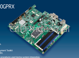
INTEL MB S5000PAL CPU BOARD - DUAL XEON 5000 5100 5300 SERIES 8-FBDIMMS SAS SATA
INTEL MB S5000PSLSATA CPU BOARD - DUAL XEON 5000 5100 SERIES 8-FBDIMMS 6SATA 3GBPS PORTS
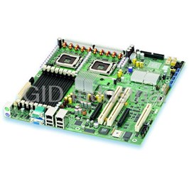
INTEL MB S5000VSA4DIMM PU BOARD - XEON 5000 5300 SERIES 4 FBDIMM SLOTS 6SATA PORTS
Request a Quote

The quote request has been received
Close

Facing challenges or have inquiries? Feel free to contact us!
Call Us +1-469-283-2440
What they say about us
FANTASTIC RESOURCE
One of our top priorities is maintaining our business with precision, and we are constantly looking for affiliates that can help us achieve our goal. With the aid of GID Industrial, our obsolete product management has never been more efficient. They have been a great resource to our company, and have quickly become a go-to supplier on our list!
Bucher Emhart Glass
EXCELLENT SERVICE
With our strict fundamentals and high expectations, we were surprised when we came across GID Industrial and their competitive pricing. When we approached them with our issue, they were incredibly confident in being able to provide us with a seamless solution at the best price for us. GID Industrial quickly understood our needs and provided us with excellent service, as well as fully tested product to ensure what we received would be the right fit for our company.
Fuji
HARD TO FIND A BETTER PROVIDER
Our company provides services to aid in the manufacture of technological products, such as semiconductors and flat panel displays, and often searching for distributors of obsolete product we require can waste time and money. Finding GID Industrial proved to be a great asset to our company, with cost effective solutions and superior knowledge on all of their materials, it’d be hard to find a better provider of obsolete or hard to find products.
Applied Materials
CONSISTENTLY DELIVERS QUALITY SOLUTIONS
Over the years, the equipment used in our company becomes discontinued, but they’re still of great use to us and our customers. Once these products are no longer available through the manufacturer, finding a reliable, quick supplier is a necessity, and luckily for us, GID Industrial has provided the most trustworthy, quality solutions to our obsolete component needs.
Nidec Vamco
TERRIFIC RESOURCE
This company has been a terrific help to us (I work for Trican Well Service) in sourcing the Micron Ram Memory we needed for our Siemens computers. Great service! And great pricing! I know when the product is shipping and when it will arrive, all the way through the ordering process.
Trican Well Service
GO TO SOURCE
When I can't find an obsolete part, I first call GID and they'll come up with my parts every time. Great customer service and follow up as well. Scott emails me from time to time to touch base and see if we're having trouble finding something.....which is often with our 25 yr old equipment.
ConAgra Foods