

 Manufacturers
INTEL D845PT

Description
Intel D845PT CPU Board - 845 Chipset Based Desktop Motherboard
Part Number
D845PT
Price
Request Quote
Manufacturer
INTEL
Lead Time
Request Quote
Category
PRODUCTS - D
Specifications
Audio Output Type
Sound card
BIOS Features
ACPI support, DMI 2.0 support, WfM 2.0 support, rapid BIOS boot
BIOS Type
AMI
Cables Included
1 x floppy cable ¦ 1 x IDE cable
Chipset Type
Intel 845
Compliant Standards
AC '97
CPU Socket Type
Socket 478
CPU Type
Pentium 4
Data Bus Speed
400 MHz
Depth
20.8 cm
Form Factor
Micro ATX
Hardware Monitoring
CPU core temperature, CPU core voltage, CPU fan tachometer, chassis temperature, system voltage
Installed Qty (Max Supported)
1
Manufacturer
Intel
Model
D845PT
MPN
BOXD845PT
Processor
Intel Pentium 4
Product Type
Motherboard
Sleep / Wake Up Features
Keyboard wake up, RTC (real-time clock) wake up, mouse wake up, suspend to RAM (STR), wake on LAN (WOL), wake on PCI device, wake on USB port, wake on modem (WOM)
Storage Controllers
ATA-100
Storage Interfaces
ATA-100 - connector(s): 2 x 40pin IDC
Supported RAM Integrity Check
ECC, Non-ECC
Supported RAM Technology
DDR SDRAM
UPC
0735858150682
Width
24.4 cm
Features
- Intel 845 Chipset
- Micro ATX
- Pentium 4
- Socket 478
Datasheet

Extracted Text
®
Intel Desktop Board
D845BG/D845PT
Technical Product Specification
November 2001
Order Number: A75852-001
®
The Intel Desktop Boards D845BG/D845PT may contain design defects or errors known as errata that may cause the product to deviate from published specifications. Current
characterized errata are documented in the Intel Desktop Board D845BG/D845PT Specification Update.
Revision History
Revision Revision History Date
®
-001 First release of the Intel Desktop Board D845BG/D845PT Technical November 2001
Product Specification.
This product specification applies to only standard D845BG and D845PT boards with BIOS
identifier PT84510A.86A.
Changes to this specification will be published in the Intel Desktop Board D845BG/D845PT
Specification Update before being incorporated into a revision of this document.
®
INFORMATION IN THIS DOCUMENT IS PROVIDED IN CONNECTION WITH INTEL PRODUCTS. EXCEPT AS
PROVIDED IN INTEL’S TERMS AND CONDITIONS OF SALE FOR SUCH PRODUCTS, INTEL ASSUMES NO LIABILITY
WHATSOEVER, AND INTEL DISCLAIMS ANY EXPRESS OR IMPLIED WARRANTY, RELATING TO SALE AND/OR USE
OF INTEL PRODUCTS INCLUDING LIABILITY OR WARRANTIES RELATING TO FITNESS FOR A PARTICULAR
PURPOSE, MERCHANTABILITY, OR INFRINGEMENT OF ANY PATENT, COPYRIGHT, OR OTHER INTELLECTUAL
PROPERTY RIGHT.
Intel Corporation may have patents or pending patent applications, trademarks, copyrights, or other intellectual property
rights that relate to the presented subject matter. The furnishing of documents and other materials and information does
not provide any license, express or implied, by estoppel or otherwise, to any such patents, trademarks, copyrights, or other
intellectual property rights.
Intel products are not intended for use in medical, life saving, or life sustaining applications or for any other application in
which the failure of the Intel product could create a situation where personal injury or death may occur.
Intel may make changes to specifications, product descriptions, and plans at any time, without notice.
®
The Intel Desktop Boards D845BG and D845PT may contain design defects or errors known as errata that may cause the
product to deviate from published specifications. Current characterized errata are available on request.
Contact your local Intel sales office or your distributor to obtain the latest specifications before placing your product order.
Copies of documents which have an ordering number and are referenced in this document, or other Intel literature, may be
obtained from:
Intel Corporation
P.O. Box 5937
Denver, CO 80217-9808
or call in North America 1-800-548-4725, Europe 44-0-1793-431-155, France 44-0-1793-421-777,
Germany 44-0-1793-421-333, other Countries 708-296-9333.
Intel and Pentium are registered trademarks of Intel Corporation or its subsidiaries in the United States and other countries.
†
Other names and brands may be claimed as the property of others.
Copyright 2001, Intel Corporation. All rights reserved.
Preface
This Technical Product Specification (TPS) specifies the board layout, components, connectors,
®
power and environmental requirements, and the BIOS for these Intel Desktop Boards: D845BG
and D845PT. It describes the standard product and available manufacturing options.
Intended Audience
The TPS is intended to provide detailed, technical information about the D845BG and D845PT
boards and their components to the vendors, system integrators, and other engineers and
technicians who need this level of information. It is specifically not intended for general
audiences.
What This Document Contains
Chapter Description
1 A description of the hardware used on the D845BG and D845PT boards
2 A map of the resources of the boards
3 The features supported by the BIOS Setup program
4 The contents of the BIOS Setup program’s menus and submenus
5 A description of the BIOS error messages, beep codes, and POST codes
Typographical Conventions
This section contains information about the conventions used in this specification. Not all of these
symbols and abbreviations appear in all specifications of this type.
Notes, Cautions, and Warnings
NOTE
✏
Notes call attention to important information.
CAUTION
Cautions are included to help you avoid damaging hardware or losing data.
WARNING
Warnings indicate conditions, which if not observed, can cause personal injury.
iii
Intel Desktop Board D845BG/D845PT Technical Product Specification
Other Common Notation
# Used after a signal name to identify an active-low signal (such as USBP0#)
(NxnX) When used in the description of a component, N indicates component type, xn are the relative
coordinates of its location on the D845BG and D845PT boards, and X is the instance of the
particular part at that general location. For example, J5J1 is a connector, located at 5J. It is
the first connector in the 5J area.
GB Gigabyte (1,073,741,824 bytes)
GB/sec Gigabytes per second
KB Kilobyte (1024 bytes)
Kbit Kilobit (1024 bits)
kbits/sec 1000 bits per second
MB Megabyte (1,048,576 bytes)
MB/sec Megabytes per second
Mbit Megabit (1,048,576 bits)
Mbit/sec Megabits per second
xxh An address or data value ending with a lowercase h indicates a hexadecimal value.
x.x V Volts. Voltages are DC unless otherwise specified.
†
This symbol is used to indicate third-party brands and names that are the property of their
respective owners.
iv
Contents
1 Product Description
1.1 Board Differences.......................................................................................................11
1.2 Overview ....................................................................................................................12
1.2.1 Feature Summary ........................................................................................12
1.2.2 Manufacturing Options .................................................................................13
1.2.3 Board Layouts..............................................................................................14
1.2.4 Block Diagram..............................................................................................16
1.3 Online Support ...........................................................................................................18
1.4 Operating System Support .........................................................................................18
1.5 Design Specifications .................................................................................................19
1.6 Processor ...................................................................................................................22
1.7 System Memory .........................................................................................................23
®
1.8 Intel 845 Chipset.......................................................................................................25
1.8.1 AGP .............................................................................................................26
1.8.2 USB..............................................................................................................27
1.8.3 IDE Support .................................................................................................29
1.8.4 Real-Time Clock, CMOS SRAM, and Battery...............................................30
®
1.8.5 Intel 82802AB 4 Mbit Firmware Hub (FWH) ...............................................30
1.9 I/O Controller..............................................................................................................30
1.9.1 Serial Ports ..................................................................................................31
1.9.2 Parallel Port..................................................................................................31
1.9.3 Diskette Drive Controller ..............................................................................32
1.9.4 Keyboard and Mouse Interface ....................................................................32
1.10 Audio Subsystem........................................................................................................33
1.10.1 Audio Connectors.........................................................................................34
1.10.2 Audio Subsystem Software ..........................................................................34
1.11 LAN Subsystem (Optional) .........................................................................................35
®
1.11.1 Intel 82562ET Platform LAN Connect Device.............................................35
1.11.2 RJ-45 LAN Connector with Integrated LEDs ................................................35
1.11.3 LAN Subsystem Software ............................................................................36
1.12 CNR (Optional)...........................................................................................................36
1.13 Hardware Management Subsystem............................................................................37
1.13.1 Hardware Monitor Component .....................................................................37
1.13.2 Fan Monitoring .............................................................................................37
1.13.3 Chassis Intrusion and Detection...................................................................38
1.14 Power Management ...................................................................................................38
1.14.1 ACPI.............................................................................................................38
1.14.2 Hardware Support ........................................................................................42
v
Intel Desktop Board D845BG/D845PT Technical Product Specification
2 Technical Reference
2.1 Introduction.................................................................................................................47
2.2 Memory Map ..............................................................................................................47
2.3 I/O Map .....................................................................................................................48
2.4 DMA Channels ...........................................................................................................50
2.5 PCI Configuration Space Map ....................................................................................50
2.6 Interrupts ....................................................................................................................51
2.7 PCI Interrupt Routing Map..........................................................................................52
2.8 Connectors.................................................................................................................54
2.8.1 Back Panel Connectors................................................................................55
2.8.2 Internal I/O Connectors ................................................................................58
2.8.3 External I/O Connectors...............................................................................71
2.9 Jumper Blocks............................................................................................................75
2.9.1 Front Panel Audio Connector/Jumper Block.................................................75
2.9.2 BIOS Setup Configuration Jumper Block......................................................76
2.10 Mechanical Considerations.........................................................................................77
2.10.1 D845BG Form Factor...................................................................................77
2.10.2 D845PT Form Factor....................................................................................78
2.10.3 I/O Shield .....................................................................................................79
2.11 Electrical Considerations ............................................................................................82
2.11.1 Power Consumption.....................................................................................82
2.11.2 Add-in Board Considerations........................................................................82
2.11.3 Standby Current Requirements....................................................................83
2.11.4 Fan Connector Current Capability ................................................................84
2.11.5 Power Supply Considerations ......................................................................84
2.12 Thermal Considerations..............................................................................................85
2.13 Reliability ....................................................................................................................87
2.14 Environmental ............................................................................................................87
2.15 Regulatory Compliance ..............................................................................................88
2.15.1 Safety Regulations .......................................................................................88
2.15.2 EMC Regulations .........................................................................................88
2.15.3 Product Certification Markings (Board Level) ...............................................89
3 Overview of BIOS Features
3.1 Introduction.................................................................................................................91
3.2 BIOS Flash Memory Organization ..............................................................................92
3.3 Resource Configuration..............................................................................................92
3.3.1 PCI Autoconfiguration ..................................................................................92
3.3.2 PCI IDE Support...........................................................................................92
3.4 System Management BIOS (SMBIOS).......................................................................93
3.5 Legacy USB Support ..................................................................................................93
3.6 BIOS Updates ............................................................................................................94
3.6.1 Language Support........................................................................................95
3.6.2 Custom Splash Screen.................................................................................95
3.7 Recovering BIOS Data ...............................................................................................95
vi
Contents
3.8 Boot Options...............................................................................................................96
3.8.1 CD-ROM and Network Boot .........................................................................96
3.8.2 Booting Without Attached Devices ...............................................................96
®
3.9 Fast Booting Systems with Intel Rapid BIOS Boot....................................................96
3.9.1 Peripheral Selection and Configuration ........................................................96
3.9.2 Intel Rapid BIOS Boot ..................................................................................97
3.10 BIOS Security Features..............................................................................................98
4 BIOS Setup Program
4.1 Introduction.................................................................................................................99
4.2 Maintenance Menu...................................................................................................100
4.2.1 Extended Configuration Submenu..............................................................101
4.3 Main Menu................................................................................................................102
4.4 Advanced Menu........................................................................................................103
4.4.1 PCI Configuration Submenu.......................................................................104
4.4.2 Boot Configuration Submenu .....................................................................105
4.4.3 Peripheral Configuration Submenu.............................................................106
4.4.4 IDE Configuration Submenu.......................................................................108
4.4.5 Diskette Configuration Submenu................................................................111
4.4.6 Event Log Configuration Submenu.............................................................112
4.4.7 Video Configuration Submenu....................................................................113
4.5 Security Menu ..........................................................................................................114
4.6 Power Menu .............................................................................................................115
4.6.1 ACPI Submenu ..........................................................................................116
4.7 Boot Menu................................................................................................................117
4.7.1 Boot Device Priority Submenu....................................................................118
4.7.2 Hard Disk Drives Submenu ........................................................................119
4.7.3 Removable Devices Submenu ...................................................................119
4.7.4 ATAPI CD-ROM Drives Submenu..............................................................120
4.8 Exit Menu .................................................................................................................120
5 Error Messages and Beep Codes
5.1 BIOS Error Messages...............................................................................................121
5.2 Port 80h POST Codes..............................................................................................123
5.3 Bus Initialization Checkpoints ...................................................................................127
5.4 Speaker ...................................................................................................................128
5.5 BIOS Beep Codes ....................................................................................................128
Figures
1. D845BG Board Components ......................................................................................14
2. D845PT Board Components.......................................................................................15
3. Block Diagram............................................................................................................16
4. Block Diagram with Optional USB 2.0 Support ...........................................................17
5. Intel 845 Chipset Block Diagram.................................................................................25
6. USB 1.1 Port Configuration ........................................................................................27
7. USB 2.0 Port Configuration (Optional)........................................................................28
8. Audio Subsystem Block Diagram................................................................................33
9. ICH2 and CNR Signal Interface..................................................................................36
vii
Intel Desktop Board D845BG/D845PT Technical Product Specification
10. Location of the Standby Power Indicator LED ............................................................44
11. Back Panel Connectors ..............................................................................................55
12. Audio Connectors.......................................................................................................59
13. Power and Hardware Control Connectors ..................................................................61
14. D845BG Add-in Board and Peripheral Interface Connectors ......................................64
15. D845PT Add-in Board and Peripheral Interface Connectors.......................................65
16. External I/O Connectors .............................................................................................71
17. Location of the Jumper Blocks....................................................................................75
18. D845BG Board Dimensions........................................................................................77
19. D845PT Board Dimensions ........................................................................................78
20. I/O Shield Dimensions (for boards with the LAN Subsystem, but not USB 2.0) ..........79
21. I/O Shield Dimensions (for boards with neither the LAN Subsystem nor USB 2.0) .....80
22. I/O Shield Dimensions (for boards without the LAN Subsystem, but with USB 2.0)....81
23. Localized High Temperature Zones............................................................................86
Tables
1. Summary of Board Differences...................................................................................11
2. Feature Summary.......................................................................................................12
3. Manufacturing Options ...............................................................................................13
4. Specifications .............................................................................................................19
5. Supported Processors ................................................................................................22
6. Supported Memory Configurations .............................................................................24
7. LAN Connector LED States........................................................................................35
8. Effects of Pressing the Power Switch .........................................................................39
9. Power States and Targeted System Power ................................................................40
10. Wake-up Devices and Events.....................................................................................41
11. Fan Connector Function/Operation.............................................................................43
12. System Memory Map..................................................................................................47
13. I/O Map ......................................................................................................................48
14. DMA Channels ...........................................................................................................50
15. PCI Configuration Space Map ....................................................................................50
16. Interrupts ....................................................................................................................51
17. PCI Interrupt Routing Map..........................................................................................53
18. PS/2 Mouse/Keyboard Connector ..............................................................................56
19. USB Connectors.........................................................................................................56
20. Parallel Port Connector...............................................................................................56
21. Serial Port A Connector..............................................................................................57
22. LAN Connector (Optional) ..........................................................................................57
23. Audio Line In Connector .............................................................................................57
24. Audio Line Out Connector ..........................................................................................57
25. Mic In Connector ........................................................................................................57
26. Auxiliary Line In Connector.........................................................................................60
27. ATAPI CD-ROM Connector ........................................................................................60
28. ATX12V Power Connector..........................................................................................62
29. Rear Chassis Fan Connector .....................................................................................62
30. Processor Fan Connector...........................................................................................62
31. Main Power Connector ...............................................................................................63
viii
Contents
32. Front Chassis Fan Connector.....................................................................................63
33. Chassis Intrusion Connector.......................................................................................63
34. CNR Connector (Optional)..........................................................................................66
35. PCI Bus Connectors...................................................................................................67
36. AGP Connector ..........................................................................................................68
37. Diskette Drive Connector............................................................................................69
38. PCI IDE Connectors ...................................................................................................70
39. SCSI LED Connector..................................................................................................70
40. Front Panel Audio Connector .....................................................................................72
41. Serial Port B Connector..............................................................................................72
42. Front Panel USB Connector .......................................................................................72
43. Auxiliary Front Panel Power/Sleep/Message-Waiting LED Connector ........................72
44. Front Panel Connector ...............................................................................................73
45. States for a One-Color Power LED.............................................................................73
46. States for a Two-Color Power LED.............................................................................74
47. Front Panel Audio Connector/Jumper Block ...............................................................76
48. BIOS Setup Configuration Jumper Settings................................................................76
49. Power Usage..............................................................................................................82
50. Standby Current Requirements ..................................................................................83
51. Fan Connector Current Capability ..............................................................................84
52. Thermal Considerations for Components ...................................................................86
53. D845BG/D845PT Board Environmental Specifications...............................................87
54. Safety Regulations .....................................................................................................88
55. EMC Regulations........................................................................................................88
56. Supervisor and User Password Functions..................................................................98
57. BIOS Setup Program Menu Bar .................................................................................99
58. BIOS Setup Program Function Keys ........................................................................100
59. Maintenance Menu...................................................................................................100
60. Extended Configuration Submenu............................................................................101
61. Main Menu................................................................................................................102
62. Advanced Menu........................................................................................................103
63. PCI Configuration Submenu .....................................................................................104
64. Boot Configuration Submenu....................................................................................105
65. Peripheral Configuration Submenu...........................................................................106
66. IDE Configuration Submenu .....................................................................................108
67. Primary/Secondary IDE Master/Slave Submenus.....................................................109
68. Diskette Configuration Submenu ..............................................................................111
69. Event Log Configuration Submenu...........................................................................112
70. Video Configuration Submenu..................................................................................113
71. Security Menu ..........................................................................................................114
72. Power Menu .............................................................................................................115
73. ACPI Submenu.........................................................................................................116
74. Boot Menu................................................................................................................117
75. Boot Device Priority Submenu..................................................................................118
76. Hard Disk Drives Submenu ......................................................................................119
77. Removable Devices Submenu..................................................................................119
78. ATAPI CD-ROM Drives Submenu ............................................................................120
79. Exit Menu .................................................................................................................120
ix
Intel Desktop Board D845BG/D845PT Technical Product Specification
80. BIOS Error Messages...............................................................................................121
81. Uncompressed INIT Code Checkpoints....................................................................123
82. Boot Block Recovery Code Checkpoints ..................................................................123
83. Runtime Code Uncompressed in F000 Shadow RAM ..............................................124
84. Bus Initialization Checkpoints ...................................................................................127
85. Upper Nibble High Byte Functions............................................................................127
86. Lower Nibble High Byte Functions............................................................................128
87. Beep Codes..............................................................................................................129
x
1 Product Description
What This Chapter Contains
1.1 Board Differences.......................................................................................................11
1.2 Overview ....................................................................................................................12
1.3 Online Support ...........................................................................................................18
1.4 Operating System Support .........................................................................................18
1.5 Design Specifications .................................................................................................19
1.6 Processor ...................................................................................................................22
1.7 System Memory .........................................................................................................23
®
1.8 Intel 845 Chipset.......................................................................................................25
1.9 I/O Controller..............................................................................................................30
1.10 Audio Subsystem........................................................................................................33
1.11 LAN Subsystem (Optional) .........................................................................................35
1.12 CNR (Optional)...........................................................................................................36
1.13 Hardware Management Subsystem............................................................................37
1.14 Power Management ...................................................................................................38
1.1 Board Differences
®
This TPS describes these Intel Desktop boards: D845BG and D845PT. The boards are identical
with the exception of the items listed in Table 1.
Table 1. Summary of Board Differences
D845BG • ATX Form Factor (12.00 inches by 8.20 inches)
(Note)
• Six PCI bus connectors
• Optional Universal Serial Bus (USB) 2.0
D845PT
• microATX Form Factor (9.60 inches by 8.20 inches)
• Three PCI bus connectors
Note: All D845BG boards with the NEC µPD720100 USB 2.0 host controller have only five PCI bus connectors.
NOTE
✏
Most of the illustrations in this document show only the D845PT board. When there are
significant differences between the two boards, illustrations of both boards are provided.
11
Intel Desktop Board D845BG/D845PT Technical Product Specification
1.2 Overview
1.2.1 Feature Summary
Table 2 summarizes the D845BG and D845PT boards’ major features.
Table 2. Feature Summary
Form Factor
D845BG: ATX (12.00 inches by 8.20 inches)
D845PT: microATX (9.60 inches by 8.20 inches)
® ®
Processor • Support for an Intel Pentium 4 processor in a µPGA478 socket
• 400 MHz system bus
Memory • Two 184-pin DDR SDRAM Dual Inline Memory Module (DIMM) sockets
• Support for single-sided or double-sided DIMMs (DDR 200 and DDR 266)
• Support for up to 2 GB system memory
NOTE: The D845BG/D845PT boards have been designed to support DIMMs based
on 512 Mbit technology for a maximum onboard capacity of up to 2 GB, but
this technology has not been validated on this board. Please refer to the
following Intel web sites. For the D845BG board:
http://developer.intel.com/design/motherbd/bg/bg_mem.htm
For the D845PT board:
http://developer.intel.com/design/motherbd/pt/pt_mem.htm
®
Chipset
Intel 845 Chipset, consisting of:
®
• Intel 82845 Memory Controller Hub (MCH)
®
• Intel 82801BA I/O Controller Hub (ICH2)
®
• Intel 82802AB 4 Mbit Firmware Hub (FWH)
Audio Audio subsystem for AC ‘97 processing using the Analog Devices AD1885 codec
Video AGP connector supporting 1.5 V 4X AGP cards
I/O Control SMSC LPC47M142 LPC Bus I/O controller
Peripheral • Up to seven USB ports
Interfaces
• Two serial ports
• One parallel port
• Two IDE interfaces with UDMA 33, ATA-66/100 support
• One diskette drive interface
†
• PS/2 keyboard and mouse ports
• Three fan connectors
Expansion • D845BG: Six PCI bus add-in card connectors (SMBus routed to PCI bus
Capabilities connector 1)
• D845PT: Three PCI bus add-in card connectors (SMBus routed to PCI bus
connector 1)
Hardware Monitor • Voltage sense to detect out of range power supply voltages
Subsystem
• Thermal sense to detect out of range thermal values
• Two fan sense inputs used to monitor fan activity
continued
12
Product Description
Table 2. Feature Summary (continued)
BIOS • Intel/AMI BIOS (resident in the Intel 82802AB 4 Mbit FWH)
• Support for Advanced Configuration and Power Interface (ACPI), Plug and Play,
and SMBIOS
Instantly Available • Support for PCI Local Bus Specification Revision 2.2
PC Technology
• Suspend to RAM support
• Wake on PCI, CNR, RS-232, front panel, PS/2 devices, and USB ports
For information about Refer to
The board’s compliance level with ACPI, Plug and Play, and SMBIOS. Section 1.5, page 19
1.2.2 Manufacturing Options
Table 3 describes the D845BG and D845PT boards’ manufacturing options. Not every
manufacturing option is available in all marketing channels. Please contact your Intel
representative to determine which manufacturing options are available to you.
Table 3. Manufacturing Options
CNR One Communication and Networking Riser (CNR) connector (slot shared with
PCI bus connector 6 on the D845BG board and with PCI bus connector 3 on the
D845PT board)
®
LAN Intel 82562ET 10/100 Mbit/sec Platform LAN Connect (PLC) device
USB 2.0
Support for USB 2.0 devices. The USB 2.0 option uses the NEC µPD720100 USB
2.0 host controller and supports up to five USB ports. This option is currently
available only on the D845BG board.
For information about Refer to
Available configurations for the D845BG and D845PT boards Section 1.3, page 18
NOTE
✏
The LAN and the CNR manufacturing options are mutually exclusive.
13
Intel Desktop Board D845BG/D845PT Technical Product Specification
1.2.3 Board Layouts
Figure 1 shows the location of the major components on the D845BG board.
A B C D
E
T
F
S
G
R
Q H
P
I
O
N M L K J
OM12997
A Audio codec K IDE connectors
B Intel 82562ET PLC device (optional) L Diskette drive connector
C AGP connector M Intel 82802AB 4 Mbit Firmware Hub (FWH)
D Back panel connectors N Speaker
E +12 V power connector (ATX12V) O Front panel connector
F Intel 82845 Memory Controller Hub (MCH) P Intel 82801BA I/O Controller Hub (ICH2)
G µPGA478 processor socket Q NEC µPD720100 USB 2.0 host controller (optional)
H DIMM sockets R Battery
I I/O controller S PCI bus add-in card connectors
J Power connector T CNR connector (optional)
Figure 1. D845BG Board Components
14
Product Description
Figure 2 shows the location of the major components on the D845PT board.
A B C D
E
S
F
R
G
Q
H
P
O
I
N M L K J
OM12986
A Audio codec K IDE connectors
B Intel 82562ET PLC device (optional) L Diskette drive connector
C AGP connector M Intel 82802AB 4 Mbit Firmware Hub (FWH)
D Back panel connectors N Speaker
E +12 V power connector (ATX12V) O Front panel connector
F Intel 82845 Memory Controller Hub (MCH) P Intel 82801BA I/O Controller Hub (ICH2)
G µPGA478 processor socket Q Battery
H DIMM sockets R PCI bus add-in card connectors
I I/O controller S CNR connector (optional)
J Power connector
Figure 2. D845PT Board Components
15
Intel Desktop Board D845BG/D845PT Technical Product Specification
1.2.4 Block Diagram
Figure 3 is a block diagram of the major functional areas of the standard D845BG and D845PT
boards. See Figure 6 on page 27 for USB port routing.
Back Panel
USB
USB Ports (2)
= connector or socket
Front Panel
USB Ports (2)
Serial Ports
LPC I/O
Parallel Port
Primary/ UDMA 33 and
Controller
Secondary IDE ATA-66/100 PS/2 Mouse
PS/2 Keyboard
Diskette Drive
µPGA478 System Bus
Connector
Processor Socket (400 MHz)
USB
LPC
Bus
845 Chipset
82801BA 82802AB 4 Mbit
82845 Memory
AHA
AGP
Controller Hub I/O Controller Hub Firmware Hub
Interface Bus
(ICH2) (FWH)
(MCH)
4X AGP
Connector
(1.5 V only)
Physical
LAN
Layer
Connector
DDR SDRAM Interface
(optional)
(optional)
Bus
DIMM Banks (2)
CSMA/CD
Unit Interface
CNR
Hardware
USB Connector
Monitor
(optional)
AC Link
SMBus
Line In
Line Out
Mic In
PCI Slot 1 PCI Bus
AD1885
Audio Codec
PCI Slot 2
Auxiliary Line In
CD-ROM
PCI Slot 3
PCI Slot 4
D845BG
PCI Slot 5
Only
Back Panel
USB
USB Ports (2)
PCI Slot 6
OM13008
Figure 3. Block Diagram
16
Product Description
Figure 4 is a block diagram of the major functional areas of the D845BG board with the USB 2.0
manufacturing option. See Figure 7 on page 28 for USB port routing.
= connector or socket
Serial Ports
LPC I/O
Parallel Port
Primary/ UDMA 33 and
Controller
PS/2 Mouse
Secondary IDE ATA-66/100
PS/2 Keyboard
Diskette Drive
µPGA478 System Bus
Connector
Processor Socket (400 MHz)
LPC
Bus
845 Chipset
82801BA 82802AB 4 Mbit
82845 Memory
AHA
AGP
Controller Hub I/O Controller Hub Firmware Hub
Interface Bus
(ICH2) (FWH)
(MCH)
4X AGP
Connector
(1.5 V only)
CSMA/CD
Unit Interface
CNR
DDR SDRAM
Connector
AC Link
Bus
DIMM Banks (2)
Line In
Line Out
Hardware AD1885
Mic In
Monitor Audio Codec
Auxiliary Line In
CD-ROM
SMBus
NEC µPD720100
Back Panel
PCI Slot 1 PCI Bus USB 2.0
USB
USB Ports (2)
Host Controller
PCI Slot 2
Front Panel
USB Ports (2)
PCI Slot 3 USB
PCI Slot 4
PCI Slot 5
OM13009
Figure 4. Block Diagram with Optional USB 2.0 Support
17
Intel Desktop Board D845BG/D845PT Technical Product Specification
1.3 Online Support
To find information about… Visit this World Wide Web site:
Intel’s D845BG and D845PT boards http://www.intel.com/design/motherbd
under “Product Info” or
“Customer Support” http://support.intel.com/support/motherboards/desktop
Available configurations for the D845BG http://developer.intel.com/design/motherbd/bg/bg_available.htm
board
Available configurations for the D845PT http://developer.intel.com/design/motherbd/pt/pt_available.htm
board
Processor data sheets http://www.intel.com/design/litcentr
ICH2 addressing http://developer.intel.com/design/chipsets/datashts
Custom splash screens http://intel.com/design/motherbd/gen_indx.htm
Audio software and utilities http://www.intel.com/design/motherbd
LAN software and drivers http://www.intel.com/design/motherbd
1.4 Operating System Support
The D845BG and D845PT boards support drivers for all of the onboard hardware and subsystems
under the following operating systems:
†
• Microsoft Windows 98 SE
• Windows ME
†
• Windows NT 4.0
• Windows 2000
• Windows XP
For information about Refer to
Supported drivers Section 1.3
NOTE
✏
Third party vendors may offer other drivers.
✏ NOTE
The USB 2.0 option requires an operating system that officially supports USB 2.0. USB 2.0
support has been tested with Windows 2000 and Windows XP drivers and is not currently
supported by any other operating system.
18
Product Description
1.5 Design Specifications
Table 4 lists the specifications applicable to the D845BG and D845PT boards.
Table 4. Specifications
Reference Specification Version, Revision Date, The information is
Name Title and Ownership available from…
AC ’97 Audio Codec ’97 Revision 2.2, ftp://download.intel.com/ial/
September 2000, scalableplatforms/ac97r22.pdf
Intel Corporation.
ACPI Advanced Configuration Version 2.0, http://www.acpi.info/spec.htm
and Power Interface July 27, 2000,
Specification Compaq Computer
Corporation,
Intel Corporation,
Microsoft Corporation,
Phoenix Technologies
Limited, and
Toshiba Corporation.
AGP Accelerated Graphics Port Revision 2.0, http://www.agpforum.org/
Interface Specification May 4, 1998, specs_specs.htm
Intel Corporation.
AMI BIOS AMIBIOS Desktop Core 7.0 AMIBIOS 7.0, http://www.ami.com/support/
August 8, 2001, doc/amibiosdesktop.pdf
American Megatrends, Inc.
ATA/ Information Technology-AT Revision 3, http://www.t13.org
ATAPI-5 Attachment with Packet February 29, 2000,
Interface - 5 Contact: T13 Chair,
(ATA/ATAPI-5) Seagate Technology.
ATX ATX Specification Version 2.03, http://www.formfactors.org/
December 1998, developer/specs/atx/
Intel Corporation. atxspecs.htm
ATX12V ATX/ATX12V Power Version 1.1, http://www.formfactors.org/
Supply Design Guide August 2000, developer/specs/atx/
Intel Corporation. atxspecs.htm
BIS Boot Integrity Services Version 1.0 for WfM 2.0 http://developer.intel.com/
August 1999, design/security/bis/
Intel Corporation. bisfaq.htm
CNR Communication and Revision 1.1, http://developer.intel.com/
Network Riser (CNR) October 18, 2000, technology/cnr/index.htm
Specification Intel Corporation.
continued
19
Intel Desktop Board D845BG/D845PT Technical Product Specification
Table 4. Specifications (continued)
Reference Specification Version, Revision Date and The information is
Name Title Ownership available from…
DDR Double Data Rate (DDR) Version 1.0, http://www.jedec.org/
SDRAM SDRAM Specification June 2000,
JEDEC Solid State Technology
Association.
Design Specification for
Revision 1.0, http://www.jedec.org/
a 184 Pin DDR
June 2000,
Unbuffered DIMM
JEDEC Solid State Technology
Association.
®
Intel JEDEC DDR Revision 0.9, http://developer.intel.com/
200/266 Unbuffered September 27, 2001, technology/memory/
DIMM Specification Intel Corporation. index.htm
Addendum
EHCI Enhanced Host Revision 0.96, http://developer.intel.com/
Controller Interface June 20, 2001, technology/usb/
Specification for Intel Corporation. ehcispec.htm
Universal Serial Bus
EPP IEEE Std 1284.1-1997 Version 1.7, http://standards.ieee.org/
(Enhanced Parallel Port) 1997, reading/ieee/std_public/
Institute of Electrical and description/busarch/
Electronic Engineers. 1284.1-1997_desc.html
El Torito Bootable CD-ROM Version 1.0, http://www.phoenix.com/
Format Specification January 25, 1995, PlatSS/products/specs.html
Phoenix Technologies Limited
and International Business
Machines Corporation.
Front Panel Front Panel I/O Version 1.0, http://www.formfactors.org/
Connectivity Design October 2000, formfactors/
Guide Intel Corporation. front_panel_io.htm
LPC Low Pin Count Interface Revision 1.0, http://www.intel.com/
Specification September 29, 1997, design/chipsets/industry/
Intel Corporation. lpc.htm
MicroATX microATX Motherboard Version 1.0, http://www.formfactors.org/
Interface Specification December 1997, developer/specs/microatx/
Intel Corporation. microatxspecs.htm
OHCI OpenHCI – Open Host Release 1.0a, http://www.usb.org/
Controller Interface October 10, 1996, developers/docs.html
Specification for USB Compaq Computer Corp.,
Microsoft Corporation, and
National Semiconductor Corp.
PCI PCI Local Bus Revision 2.2, http://www.pcisig.com/
Specification December 18, 1998, specifications
PCI Special Interest Group.
PCI Bus Power Revision 1.1, http://www.pcisig.com/
Management Interface December 18, 1998, specifications
Specification PCI Special Interest Group.
continued
20
Product Description
Table 4. Specifications (continued)
Reference Specification Version, Revision Date The information is
Name Title and Ownership available from…
Plug and Plug and Play BIOS Version 1.0a, http://www.microsoft.com/
Play Specification May 5, 1994, hwdev/respec/
Compaq Computer Corporation, pnpspecs.htm
Phoenix Technologies Limited,
and Intel Corporation.
PXE Preboot Execution Version 2.1, ftp://download.intel.com/ial/
Environment September 20, 1999, wfm/pxespec.pdf
Intel Corporation.
SFX SFX/SFX12V Power Version 2.0, http://www.formfactors.org/
Supply Design Guide May 2001, developer/specs/sfx/
Intel Corporation. sfx12v.pdf
SMBIOS System Management Version 2.3.1, http://www.dmtf.org/
BIOS March 16, 1999, download/standards/
American Megatrends DSP0119.pdf
Incorporated,
Award Software International
Incorporated,
Compaq Computer Corporation,
Dell Computer Corporation,
Hewlett-Packard Company,
Intel Corporation,
International Business Machines
Corporation,
Phoenix Technologies Limited,
and SystemSoft Corporation.
UHCI Universal Host Controller Revision 1.1, http://www.usb.org/
Interface Design Guide March 1996, developers/docs.html
Intel Corporation.
USB Universal Serial Bus Revision 1.1, http://www.usb.org/
Specification September 23, 1998, developers/docs.html
Compaq Computer Corporation,
Intel Corporation,
Microsoft Corporation, and
NEC Corporation.
Revision 2.0, http://www.usb.org/
April 27, 2000, developers/docs.html
Compaq Computer Corporation,
Hewlett-Packard Company,
Lucent Technologies Inc.,
Intel Corporation,
Microsoft Corporation,
NEC Corporation, and
Koninklijke Philips Electronics
N.V.
WfM Wired for Management Version 2.0, http://developer.intel.com/
Baseline December 18, 1998, ial/WfM/wfmspecs.htm
Intel Corporation.
21
Intel Desktop Board D845BG/D845PT Technical Product Specification
1.6 Processor
CAUTION
Use only the processors listed below. Use of unsupported processors can damage the board, the
®
processor, and the power supply. See the Intel Desktop Board D845BG/D845PT Specification
Update for the most up-to-date list of supported processors for these boards.
The D845BG and D845PT boards support a single Pentium 4 processor (in a µPGA478 socket)
with a system bus of 400 MHz. The D845BG and D845PT boards support the processors listed in
Table 5. All supported onboard memory can be cached, up to the cachability limit of the
processor. See the processor’s data sheet for cachability limits.
Table 5. Supported Processors
Type Designation System Bus L2 Cache Size
Pentium 4 processor 1.5, 1.6, 1.7, 1.8, 1.9, 400 MHz 256 KB
and 2.0 GHz
NOTE
✏
Use only ATX12V- or SFX12V-compliant power supplies with the D845BG and D845PT boards.
ATX12V and SFX12V power supplies have an additional power lead that provides required
supplemental power for the Intel Pentium 4 processor. Always connect the 20-pin and 4-pin leads
of ATX12V and SFX12V power supplies to the corresponding connectors on the D845BG and
D845PT boards, otherwise the board will not boot.
Do not use a standard ATX power supply. The board will not boot with a standard ATX power
supply.
For information about Refer to
Processor support Section 1.3, page 18
Processor usage Section 1.3, page 18
Power supply connectors Section 2.8.2.3, page 61
22
Product Description
1.7 System Memory
NOTE
✏
Remove the AGP video card before installing or upgrading memory to avoid interference with the
memory retention mechanism.
NOTE
✏
The D845BG/D845PT boards have been designed to support DIMMs based on 512 Mbit
technology for a maximum onboard capacity of up to 2 GB, but this technology has not been
validated on this board. Please refer to the following Intel web sites for the latest lists of tested
memory.
For the D845BG board:
http://developer.intel.com/design/motherbd/bg/bg_mem.htm
For the D845PT board:
http://developer.intel.com/design/motherbd/pt/pt_mem.htm
The D845BG and D845PT boards both have two DIMM sockets and support the following
memory features:
• 2.5 V (only) 184-pin DDR SDRAM DIMMs with gold-plated contacts
• Unbuffered single-sided or double-sided DIMMs
• Maximum total system memory: 2 GB; minimum total system memory: 64 MB
• 200/266 MHz DDR SDRAM DIMMs only
• Serial Presence Detect (SPD)
• Suspend to RAM
• Non-ECC and ECC DIMMs
NOTE
✏
To be fully compliant with all applicable DDR SDRAM memory specifications, the board should be
populated with DIMMs that support the Serial Presence Detect (SPD) data structure. This allows
the BIOS to read the SPD data and program the chipset to accurately configure memory settings
for optimum performance. If non-SPD memory is installed, the BIOS will attempt to correctly
configure the memory settings, but performance and reliability may be impacted or the DIMMs
may not function under the determined frequency.
NOTE
✏
For ECC functionality, all installed DIMMs must be ECC. If both ECC and non-ECC DIMMs are
used, ECC will not function.
For information about Refer to
Obtaining DDR SDRAM specifications Section 1.5, page 19
23
Intel Desktop Board D845BG/D845PT Technical Product Specification
Table 6 lists the supported DIMM configurations.
Table 6. Supported Memory Configurations
DIMM Number of DDR SDRAM DDR SDRAM Organization Number of DDR
Capacity Sides Density Front-side/Back-side SDRAM Devices
64 MB SS 64 Mbit 8 M x 8/empty 8
64 MB SS 128 Mbit 8 M x 16/empty 4
(Notes 1 and 2)
96 MB DS 64 Mbit 8 M x 8/4 M x 16 12
(Notes 1 and 2)
96 MB DS 128/64 Mbit 8 M x 16/4 M x 16 8
(Note 1)
128 MB DS 64 Mbit 8 M x 8/8 M x 8 16
(Notes 1 and 2)
128 MB DS 128 Mbit 8 M x 16/8 M x 16 8
128 MB SS 128 Mbit 16 M x 8/empty 8
128 MB SS 256 Mbit 16 M x 16/empty 4
(Notes 1 and 2)
192 MB DS 128 Mbit 16 M x 8/8 M x 16 12
(Notes 1 and 2)
192 MB DS 128/64 Mbit 16 M x 8/8 M x 8 16
(Notes 1 and 2)
256 MB DS 128 Mbit 16 M x 8/16 M x 8 16
(Notes 1 and 2)
256 MB DS 256 Mbit 16 M x 16/16 M x 16 8
256 MB SS 256 Mbit 32 M x 8/empty 8
(Notes 1 and 2)
512 MB DS 256 Mbit 32 M x 8/32 M x 8 16
Notes:
1. If the number of DDR SDRAM devices is greater than nine, the DIMM will be double sided.
2. Front side population/back side population indicated for DDR SDRAM density and DDR SDRAM organization.
3. In the second column, “DS” refers to double-sided memory modules (containing two rows of DDR SDRAM) and “SS”
refers to single-sided memory modules (containing one row of DDR SDRAM).
24
Product Description
®
1.8 Intel 845 Chipset
The Intel 845 chipset consists of the following devices:
• Intel 82845 Memory Controller Hub (MCH) with Accelerated Hub Architecture (AHA) bus
• Intel 82801BA I/O Controller Hub (ICH2) with AHA bus
• Intel 82802AB Firmware Hub (FWH)
The MCH is a centralized controller for the system bus, the memory bus, the AGP bus, and the
Accelerated Hub Architecture interface. The ICH2 is a centralized controller for the board’s I/O
paths. The FWH provides the nonvolatile storage of the BIOS. The component combination
provides the chipset interfaces as shown in Figure 5.
UDMA 33
Network
ATA-66/100
System Bus USB
845 Chipset
82845 82801BA 82802AB 4 Mbit
AHA
Memory Controller I/O Controller Hub Firmware Hub
Bus
Hub (MCH) (ICH2) (FWH)
LPC Bus
AGP DDR SDRAM
SMBus PCI Bus AC Link
Bus
Interface
OM13069
Figure 5. Intel 845 Chipset Block Diagram
NOTE
✏
The USB bus is routed from the NEC USB 2.0 controller if the USB 2.0 option is supported.
For information about Refer to
The Intel 845 chipset http://developer.intel.com
Resources used by the chipset Chapter 2
25
Intel Desktop Board D845BG/D845PT Technical Product Specification
1.8.1 AGP
NOTE
✏
The AGP connector is keyed for 1.5 V AGP cards only. Do not attempt to install a legacy 3.3 V
AGP card. The AGP connector is not mechanically compatible with legacy 3.3 V AGP cards.
The AGP connector supports AGP add-in cards with 1.5 V Switching Voltage Level (SVL).
Legacy 3.3 V AGP cards are not supported.
For information about Refer to
The location of the AGP connector Figure 1, page 14
The signal names of the AGP connector Table 36, page 68
AGP is a high-performance interface for graphics-intensive applications, such as 3D applications.
While based on the PCI Local Bus Specification, Rev. 2.2, AGP is independent of the PCI bus and
is intended for exclusive use with graphical display devices. AGP overcomes certain limitations of
the PCI bus related to handling large amounts of graphics data with the following features:
• Pipelined memory read and write operations that hide memory access latency
• Demultiplexing of address and data on the bus for nearly 100 percent efficiency
For information about Refer to
Obtaining the Accelerated Graphics Port Interface Specification Section 1.5, page 19
26
Product Description
1.8.2 USB
The following sections describe the USB port configurations implemented on the
D845BG/D845PT boards.
NOTE
✏
Computer systems that have an unshielded cable attached to a USB port may not meet FCC
Class B requirements, even if no device is attached to the cable. Use shielded cable that meets the
requirements for full-speed devices.
For information about Refer to
The location of the USB connectors on the back panel Figure 11, page 55
The signal names of the back panel USB connectors Table 19, page 56
The location of the front panel USB connector Figure 16, page 71
The signal names of the front panel USB connector Table 42, page 72
The front panel, UHCI, and USB specifications Section 1.5, page 19
1.8.2.1 USB 1.1 Support
The D845BG/D845PT boards support up to seven USB ports, as shown in Figure 6. The ICH2
provides four ports, three of which are user-accessible:
• Two ports implemented with stacked back panel connectors, adjacent to the PS/2 connectors
• One port accessible through an optional CNR connector
• One port routed to the SMSC USB hub
The onboard SMSC USB hub provides four ports:
• Two ports implemented with stacked back panel connectors, adjacent to the audio connectors
• Two ports routed to the front panel USB connector
For more than seven USB devices, an external hub can be connected to any of the ports.
Back panel USB connectors
USB USB ports (2)
adjacent to the PS/2 ports
82801BA
I/O Controller Hub
(ICH2)
USB port accesible through a USB
USB CNR connector
connector on an optional CNR add-in card
USB
Back panel USB connectors
USB USB ports (2)
adjacent to the audio connectors
SMSC LPC47M142
LPC Bus
I/O Controller
Front panel USB
USB USB ports (2)
connectors
OM12339
Figure 6. USB 1.1 Port Configuration
27
Intel Desktop Board D845BG/D845PT Technical Product Specification
1.8.2.2 USB 2.0 Support (Optional)
✏ NOTE
The USB 2.0 option is currently available only on the D845BG board. All D845BG boards with
the NEC µPD720100 USB 2.0 host controller have only five PCI bus connectors.
The D845BG board supports USB 2.0 using the NEC µPD720100 USB 2.0 host controller, which
is a manufacturing option. The port routing is implemented as shown in Figure 7. The NEC
µPD720100 controller is connected through the PCI bus and provides support for up to five USB
ports:
• Two ports implemented with stacked back panel connectors, adjacent to the audio connectors
• Two ports routed to the front panel USB connector
• One port accessible through the CNR connector
For more than five USB devices, an external hub can be connected to any of the ports. D845BG
boards with the USB 2.0 option fully support OHCI and EHCI and use OHCI- and
EHCI-compatible drivers.
✏ NOTE
The USB 2.0 option requires an operating system that officially supports USB 2.0. USB 2.0
support has been tested with Windows 2000 and Windows XP drivers and is not currently
supported by any other operating system.
Back panel USB connectors
USB ports (2)
adjacent to the audio connectors
NEC µPD720100
USB port accesible through a USB
PCI USB 2.0 USB CNR connector
connector on an optional CNR add-in card
Host Controller
USB ports (2) Front panel USB connectors
OM12337
Figure 7. USB 2.0 Port Configuration (Optional)
28
Product Description
1.8.3 IDE Support
1.8.3.1 IDE Interfaces
The ICH2’s IDE controller has two independent bus-mastering IDE interfaces that can be
independently enabled. The IDE interfaces support the following modes:
• Programmed I/O (PIO): processor controls data transfer.
• 8237-style DMA: DMA offloads the processor, supporting transfer rates of up to 16 MB/sec.
• Ultra DMA: DMA protocol on IDE bus supporting host and target throttling and transfer rates
of up to 33 MB/sec.
• ATA-66: DMA protocol on IDE bus supporting host and target throttling and transfer rates of
up to 66 MB/sec. ATA-66 protocol is similar to Ultra DMA and is device driver compatible.
• ATA-100: DMA protocol on IDE bus allows host and target throttling. The ICH2’s ATA-100
logic can achieve read transfer rates up to 100 MB/sec and write transfer rates up to 88 MB/sec.
✏ NOTE
ATA-66 and ATA-100 are faster timings and require a specialized cable to reduce reflections,
noise, and inductive coupling.
The IDE interfaces also support ATAPI devices (such as CD-ROM drives) and ATA devices using
the transfer modes listed in Section 4.4.4.1 on page 109.
The BIOS supports Logical Block Addressing (LBA) and Extended Cylinder Head Sector (ECHS)
translation modes. The drive reports the transfer rate and translation mode to the BIOS.
The D845BG and D845PT boards support Laser Servo (LS-120) diskette technology through the
IDE interfaces. An LS-120 drive can be configured as a boot device by setting the BIOS Setup
program’s Boot menu to one of the following:
• ARMD-FDD (ATAPI removable media device – floppy disk drive)
• ARMD-HDD (ATAPI removable media device – hard disk drive)
For information about Refer to
The location of the IDE connectors Figure 14, page 64
The signal names of the IDE connectors Table 38, page 70
BIOS Setup program’s Boot menu Table 74, page 117
1.8.3.2 SCSI Hard Drive Activity LED Connector
The SCSI hard drive activity LED connector is a 1 x 2-pin connector that allows an add-in
SCSI controller to use the same LED as the onboard IDE controller. For proper operation, this
connector should be wired to the LED output of the add-in SCSI controller. The LED indicates
when data is being read from, or written to, both the add-in SCSI controller and the IDE controller.
For information about Refer to
The location of the SCSI hard drive activity LED connector Figure 14, page 64, or
Figure 15, page 65
The signal names of the SCSI hard drive activity LED connector Table 39, page 70
29
Intel Desktop Board D845BG/D845PT Technical Product Specification
1.8.4 Real-Time Clock, CMOS SRAM, and Battery
The real-time clock provides a time-of-day clock and a multicentury calendar with alarm features.
The real-time clock supports 256 bytes of battery-backed CMOS SRAM in two banks that are
reserved for BIOS use.
A coin-cell battery (CR2032) powers the real-time clock and CMOS memory. When the computer
is not plugged into a wall socket, the battery has an estimated life of three years. When the
computer is plugged in, the standby current from the power supply extends the life of the battery.
The clock is accurate to ± 13 minutes/year at 25 ºC with 3.3 VSB applied.
The time, date, and CMOS values can be specified in the BIOS Setup program. The CMOS values
can be returned to their defaults by using the BIOS Setup program.
✏ NOTE
If the battery and AC power fail, custom defaults, if previously saved, will be loaded into CMOS
RAM at power-on.
®
1.8.5 Intel 82802AB 4 Mbit Firmware Hub (FWH)
The FWH provides the following:
• System BIOS program
• Logic that enables protection for storing and updating of platform information
1.9 I/O Controller
The SMSC LPC47M142 I/O controller provides the following features:
• Two serial ports
• One parallel port with Extended Capabilities Port (ECP) and Enhanced Parallel Port
(EPP) support
• Serial IRQ interface compatible with serialized IRQ support for PCI systems
• PS/2-style mouse and keyboard interfaces
• Interface for one 1.2 MB or 1.44 MB diskette drive
• Intelligent power management, including a programmable wake-up event interface
• PCI power management support
• Two fan tachometer inputs
• Integrated USB hub
The BIOS Setup program provides configuration options for the I/O controller.
For information about Refer to
SMSC LPC47M142 I/O controller http://www.smsc.com
30
Product Description
1.9.1 Serial Ports
The D845BG and D845PT boards have two serial port connectors. Serial port A is located on the
back panel. Serial port B is accessible using a connector located near the main power connector.
The serial ports’ NS16C550-compatible UART supports data transfers at speeds up to
115.2 kbits/sec with BIOS support. The serial ports can be assigned as COM1 (3F8h),
COM2 (2F8h), COM3 (3E8h), or COM4 (2E8h).
For information about Refer to
The location of the serial port A connector Figure 11, page 55
The signal names of the serial port A connector Table 21, page 57
The location of the serial port B connector Figure 16, page 71
The signal names of the serial port B connector Table 41, page 72
1.9.2 Parallel Port
The 25-pin D-Sub parallel port connector is located on the back panel. In the BIOS Setup
program, the parallel port can be set to the following modes:
†
• Output only (PC AT -compatible mode)
• Bi-directional (PS/2 compatible)
• EPP
• ECP
For information about Refer to
The location of the parallel port connector Figure 11, page 55
The signal names of the parallel port connector Table 20, page 56
Setting the parallel port’s mode Table 65, page 106
31
Intel Desktop Board D845BG/D845PT Technical Product Specification
1.9.3 Diskette Drive Controller
The I/O controller supports one diskette drive that is compatible with the 82077 diskette drive
controller and supports both PC-AT and PS/2 modes.
For information about Refer to
The location of the diskette drive connector Figure 14, page 64
The signal names of the diskette drive connector Table 37, page 69
The supported diskette drive capacities and sizes Table 68, page 111
1.9.4 Keyboard and Mouse Interface
PS/2 keyboard and mouse connectors are located on the back panel. The +5 V lines to these
†
connectors are protected with a PolySwitch circuit that, like a self-healing fuse, reestablishes the
connection after an overcurrent condition is removed.
NOTE
✏
The keyboard is supported in the bottom PS/2 connector and the mouse is supported in the top
PS/2 connector. Power to the computer should be turned off before a keyboard or mouse is
connected or disconnected.
The keyboard controller contains the AMI keyboard and mouse controller code, provides the
keyboard and mouse control functions, and supports password protection for power-on/reset. A
power-on/reset password can be specified in the BIOS Setup program.
For information about Refer to
The location of the keyboard and mouse connectors Figure 11, page 55
The signal names of the keyboard and mouse connectors Table 18, page 56
32
Product Description
1.10 Audio Subsystem
The audio subsystem includes these features:
• Split digital/analog architecture for improved S/N (signal-to-noise) ratio: ≥ 85 dB
• Power management support for ACPI 2.0 (driver dependant)
• Mic in pre-amp that supports dynamic, condenser, and electret microphones
The audio subsystem supports the following audio interfaces:
• ATAPI-style connectors:
Auxiliary line in
CD-ROM
• Front panel audio connector, including pins for:
Line out
Mic in
• Back panel audio connectors:
Line out
Line in
Mic in
The audio subsystem consists of the following devices:
• Intel 82801BA I/O Controller Hub (ICH2)
• Analog Devices AD1885 audio codec
Figure 8 is a block diagram of the audio subsystem.
Line In
Line Out
82801BA
AC ’97 AD1885
I/O Controller Hub Mic In
Link Audio Codec
(ICH2)
Auxiliary Line In
CD-ROM
OM13010
Figure 8. Audio Subsystem Block Diagram
For information about Refer to
Upgrading the onboard audio subsystem using a CNR audio card Section 1.12, page 36
The front panel audio connector Section 2.8.3, page 71
The back panel audio connectors Section 2.8.1, page 55
33
Intel Desktop Board D845BG/D845PT Technical Product Specification
1.10.1 Audio Connectors
1.10.1.1 Front Panel Audio Connector
A 2 x 5-pin connector provides mic in and line out signals for front panel audio connectors.
For information about Refer to
The location of the connector Section 2.8.3, page 71
The signal names of the front panel audio connector Table 40, page 72
Obtaining the Front Panel I/O Connectivity Design Guide Section 1.5, page 19
NOTE
✏
The front panel audio connector is alternately used as a jumper block for routing audio signals.
Refer to Section 2.9.1 on page 75 for more information.
1.10.1.2 Auxiliary Line In Connector
A 1 x 4-pin ATAPI-style connector connects the left and right channel signals of an internal audio
device to the audio subsystem.
For information about Refer to
The location of the auxiliary line in connector Figure 12, page 59
The signal names of the auxiliary line in connector Table 27, page 60
1.10.1.3 ATAPI CD-ROM Audio Connector
A 1 x 4-pin ATAPI-style connector connects an internal ATAPI CD-ROM drive to the audio
mixer.
For information about Refer to
The location of the ATAPI CD-ROM connector Figure 12, page 59
The signal names of the ATAPI CD-ROM connector Table 27, page 60
1.10.2 Audio Subsystem Software
Audio software and drivers are available from Intel’s World Wide Web site.
For information about Refer to
Obtaining audio software and drivers Section 1.3, page 18
34
Product Description
1.11 LAN Subsystem (Optional)
The Network Interface Controller subsystem consists of the ICH2 (with integrated LAN Media
Access Controller) and a physical layer interface device. Features of the LAN subsystem include:
• PCI Bus Master interface
• CSMA/CD Protocol Engine
• Serial CSMA/CD unit interface that supports the 82562ET (10/100 Mbit/sec Ethernet) on the
CNR bus
• PCI Power Management
Supports ACPI technology
Supports LAN wake capabilities
®
1.11.1 Intel 82562ET Platform LAN Connect Device
The Intel 82562ET component provides an interface to the back panel RJ-45 connector with
integrated LEDs. This physical interface may alternately be provided through the CNR connector.
The Intel 82562ET provides the following functions:
• Basic 10/100 Ethernet LAN connectivity
• Supports RJ-45 connector with status indicator LEDs on the back panel
• Full device driver compatibility
• ACPI support
• Programmable transit threshold
• Configuration EEPROM that contains the MAC address
1.11.2 RJ-45 LAN Connector with Integrated LEDs
Two LEDs are built into the RJ-45 LAN connector. Table 7 describes the LED states when the
board is powered up and the LAN subsystem is operating.
Table 7. LAN Connector LED States
LED Color LED State Condition
Green Off 10 Mbit/sec data rate is selected.
On 100 Mbit/sec data rate is selected.
Yellow Off LAN link is not established.
On (steady state) LAN link is established.
On (brighter and pulsing) The computer is communicating with another computer on
the LAN.
35
Intel Desktop Board D845BG/D845PT Technical Product Specification
1.11.3 LAN Subsystem Software
LAN software and drivers are available from Intel’s World Wide Web site.
For information about Refer to
Obtaining LAN software and drivers Section 1.3, page 18
1.12 CNR (Optional)
The CNR connector provides an interface that supports the audio, modem, USB, and LAN
interfaces of the Intel 845 chipset. Figure 9 shows the signal interface between the riser and
the ICH2.
AC ’97 Interface Communication and
Networking Riser
Intel 82801BA
LAN Interface
I/O Controller Hub
SMBus (Up to two AC ’97 codecs
(ICH2)
and one LAN device)
USB
OM12277
Figure 9. ICH2 and CNR Signal Interface
NOTE
✏
The USB bus is routed from the NEC USB 2.0 controller if the USB 2.0 option is supported.
The interfaces supported by the CNR include the following:
• AC ’97 interface: supports audio and/or modem functions on the CNR card.
• LAN interfaces: an eight-pin interface for use with Platform LAN Connection (PLC) based
devices.
• SMBus interface: provides Plug-and-Play functionality for the CNR card.
• USB interface: provides a USB interface for the CNR card.
The CNR connector includes power signals required for power management and for CNR card
operation. To learn more about the CNR, refer to the CNR specification.
The onboard two-channel audio subsystem can be upgraded to four- or six-channel audio using a
CNR audio upgrade card in a slave configuration. CNR audio upgrade cards are available in
multiple configurations from several different vendors supporting analog or S/P-DIF digital
connections. A list of vendors supplying CNR audio upgrade cards compatible with the
D845BG/D845PT boards’ onboard audio subsystem, as well as an installation guide for these cards
with SoundMAX with SPX are available on the following web site:
http://developer.intel.com/technology/cnr/
36
CNR Connector
Product Description
NOTE
✏
If you install a CNR card that cannot support a multichannel audio upgrade, the D845BG and
D845PT boards’ integrated audio codec will be disabled. This only applies to D845BG and
D845PT boards that have both the onboard audio subsystem and a CNR.
NOTE
✏
The brand and type of audio codec used on the CNR card must match that of the D845BG/D845PT
boards’ codec (Analog Devices AD1885).
For information about Refer to
Obtaining the CNR specification Section 1.5, page 19
1.13 Hardware Management Subsystem
The hardware management features enable the boards to be compatible with the Wired for
Management (WfM) specification. The board has several hardware management features,
including the following:
• Fan monitoring
• Thermal and voltage monitoring
• Chassis intrusion detection
For information about Refer to
The WfM specification Section 1.5, page 19
1.13.1 Hardware Monitor Component
The hardware monitor component provides low-cost instrumentation capabilities. The features of
the component include:
• Internal ambient temperature sensing
• Remote thermal diode sensing for direct monitoring of processor temperature
• Power supply monitoring (+5 V, +3.3 V, +1.5 V, 3.3 VSB, and Vccp) to detect levels above or
below acceptable values
• SMBus interface
1.13.2 Fan Monitoring
The SMSC LPC47M142 I/O controller provides two fan tachometer inputs. Monitoring can be
®
implemented using Intel Active Monitor or third-party software.
For information about Refer to
The functions of the fan connectors Section 1.14.2.2, page 43
The location of the fan connectors Figure 13, page 61
The signal names of the fan connectors Section 2.8.2.3, page 61
37
Intel Desktop Board D845BG/D845PT Technical Product Specification
1.13.3 Chassis Intrusion and Detection
The boards support a chassis security feature that detects if the chassis cover is removed. For the
chassis intrusion circuit to function, the chassis’ power supply must be connected to AC power.
The security feature uses a mechanical switch on the chassis that attaches to the chassis intrusion
connector. The mechanical switch is closed for normal computer operation.
For information about Refer to
The location of the chassis intrusion connector Figure 13, page 61
The signal names of the chassis intrusion connector Table 33, page 63
NOTE
✏
Chassis intrusion detection may be implemented using Intel Active Monitor or third-party
software.
1.14 Power Management
Power management is implemented at several levels, including:
• Software support through Advanced Configuration and Power Interface (ACPI)
• Hardware support:
Power connector
Fan connectors
LAN wake capabilities
Instantly Available PC technology
Resume on Ring
Wake from USB
Wake from PS/2 devices
Power Management Event (PME#) wake-up support
1.14.1 ACPI
ACPI gives the operating system direct control over the power management and Plug and Play
functions of a computer. The use of ACPI with the D845BG and D845PT boards requires an
operating system that provides full ACPI support. ACPI features include:
• Plug and Play (including bus and device enumeration)
• Power management control of individual devices, add-in boards (some add-in boards may
require an ACPI-aware driver), video displays, and hard disk drives
• Methods for achieving less than 15-watt system operation in the power-on/standby
sleeping state
• A Soft-off feature that enables the operating system to power-off the computer
• Support for multiple wake-up events (see Table 10 on page 41)
• Support for a front panel power and sleep mode switch
38
Product Description
Table 8 lists the system states based on how long the power switch is pressed, depending on how
ACPI is configured with an ACPI-aware operating system.
Table 8. Effects of Pressing the Power Switch
…and the power switch is
If the system is in this state… pressed for …the system enters this state
Off Less than four seconds Power-on
(ACPI G2/G5 – Soft off)
(ACPI G0 – working state)
On Less than four seconds Soft-off/Standby
(ACPI G0 – working state)
(ACPI G1 – sleeping state)
On More than four seconds Fail safe power-off
(ACPI G0 – working state)
(ACPI G2/G5 – Soft off)
Sleep Less than four seconds Wake-up
(ACPI G1 – sleeping state)
(ACPI G0 – working state)
Sleep More than four seconds Power-off
(ACPI G1 – sleeping state)
(ACPI G2/G5 – Soft off)
For information about Refer to
The D845BG and D845PT boards’ compliance level with ACPI Section 1.5, page 19
39
Intel Desktop Board D845BG/D845PT Technical Product Specification
1.14.1.1 System States and Power States
Under ACPI, the operating system directs all system and device power state transitions. The
operating system puts devices in and out of low-power states based on user preferences and
knowledge of how devices are being used by applications. Devices that are not being used can be
turned off. The operating system uses information from applications and user settings to put the
system as a whole into a low-power state.
Table 9 lists the power states supported by the D845BG and D845PT boards along with the
associated system power targets. See the ACPI specification for a complete description of the
various system and power states.
Table 9. Power States and Targeted System Power
Processor Targeted System
(Note 1)
Global States Sleeping States States Device States Power
G0 – working S0 – working C0 – working D0 – working Full power > 30 W
state state.
G1 – sleeping S1 – Processor C1 – stop D1, D2, D3 – 5 W < power < 52.5 W
state stopped grant device
specification
specific.
(Note 2)
G1 – sleeping S3 – Suspend to No power D3 – no power Power < 5 W
state RAM. Context except for
saved to RAM. wake-up logic.
(Note 2)
G1 – sleeping S4 – Suspend to No power D3 – no power Power < 5 W
state disk. Context except for
saved to disk. wake-up logic.
(Note 2)
G2/S5 S5 – Soft off. No power D3 – no power Power < 5 W
Context not saved. except for
Cold boot is wake-up logic.
required.
G3 – No power to the No power D3 – no power for No power to the system.
mechanical off system. wake-up logic, Service can be performed
except when safely.
AC power is
provided by
disconnected
battery or external
from the
source.
computer.
Notes:
1. Total system power is dependent on the system configuration, including add-in boards and peripherals powered
by the system chassis’ power supply.
2. Dependent on the standby power consumption of wake-up devices used in the system.
40
Product Description
1.14.1.2 Wake-up Devices and Events
Table 10 lists the devices or specific events that can wake the computer from specific states.
Table 10. Wake-up Devices and Events
These devices/events can wake up the computer… …from this state
Power switch S1, S3, S4, S5
RTC alarm S1, S3, S4, S5
(Note 1)
LAN S1, S3, S4, S5
(Note 2) (Note 2)
CNR S1, S3, S4 , S5
PME# S1, S3, S4, S5
Modem (back panel Serial Port A) S1, S3
USB S1, S3
PS/2 devices S1, S3
Notes:
1. For LAN and PME#, S5 is disabled by default in the BIOS Setup program. Setting this option to Power On will
enable a wake-up event from LAN in the S5 state.
2. Except from the CNR’s USB interface.
NOTE
✏
The use of these wake-up events from an ACPI state requires an operating system that provides full
ACPI support. In addition, software, drivers, and peripherals must fully support ACPI wake
events.
1.14.1.3 Plug and Play
In addition to power management, ACPI provides control information so that operating systems
can facilitate Plug and Play. ACPI is used only to configure devices that do not use other hardware
configuration standards. PCI devices for example, are not configured by ACPI.
41
Intel Desktop Board D845BG/D845PT Technical Product Specification
1.14.2 Hardware Support
CAUTION
Ensure that the power supply provides adequate +5 V standby current if LAN wake capabilities
and Instantly Available PC technology features are used. Failure to do so can damage the power
supply. The total amount of standby current required depends on the wake devices supported and
manufacturing options. Refer to Section 2.11.3 on page 83 for additional information.
The D845BG and D845PT boards provide several power management hardware features,
including:
• Power connector
• Fan connectors
• LAN wake capabilities
• Instantly Available PC technology
• Resume on Ring
• Wake from USB
• Wake from PS/2 keyboard
• PME# wake-up support
LAN wake capabilities and Instantly Available PC technology require power from the +5 V
standby line. The sections discussing these features describe the incremental standby power
requirements for each.
Resume on Ring enables telephony devices to access the computer when it is in a power-managed
state. The method used depends on the type of telephony device (external or internal).
NOTE
✏
The use of Resume on Ring and Wake from USB technologies from an ACPI state requires an
operating system that provides full ACPI support.
1.14.2.1 Power Connector
When used with an ATX12V- or SFX12V-compliant power supply that supports remote power
on/off, the D845BG and D845PT boards can turn off the system power through software control.
When the system BIOS receives the correct command from the operating system, the BIOS turns
off power to the computer.
With soft-off enabled, if power to the computer is interrupted by a power outage or a disconnected
power cord, when power resumes, the computer returns to the power state it was in before power
was interrupted (on or off). The computer’s response can be set using the After Power Failure
feature in the BIOS Setup program’s Boot menu.
For information about Refer to
The location of the power connector Figure 13, page 61
The signal names of the power connector Table 31, page 63
The BIOS Setup program’s Boot menu Table 74, page 117
The ATX and SFX specifications Section 1.5, page 19
42
Product Description
1.14.2.2 Fan Connectors
Table 11 summarizes the function/operation of the fan connectors.
Table 11. Fan Connector Function/Operation
Connector Description
Processor fan • +12 V DC connection for a processor fan or active fan heatsink.
• Fan is on in the S0 or S1 state.
Fan is off when the system is off or in the S3, S4, or S5 state.
• Wired to a fan tachometer input of the SMSC LPC47M142 I/O controller.
Front chassis fan • +12 V DC connection for a system or chassis fan.
• Fan is on in the S0 or S1 state.
Fan is off when the system is off or in the S3, S4, or S5 state.
• Wired to a fan tachometer input of the SMSC LPC47M142 I/O controller.
Rear chassis fan • +12 V DC connection for a system or chassis fan.
• Fan is on in the S0 or S1 state.
Fan is off when the system is off or in the S3, S4, or S5 state.
For information about Refer to
The location of the fan connectors Figure 13, page 61
The signal names of the fan connectors Section 2.8.2.3, page 61
1.14.2.3 LAN Wake Capabilities
CAUTION
For LAN wake capabilities, the 5-V standby line for the power supply must be capable of providing
adequate +5 V standby current. Failure to provide adequate standby current when implementing
LAN wake capabilities can damage the power supply. Refer to Section 2.11.3 on page 83 for
additional information.
LAN wake capabilities enable remote wake-up of the computer through a network. The LAN
subsystem PCI bus network adapter monitors network traffic at the Media Independent Interface.
†
Upon detecting a Magic Packet frame, the LAN subsystem asserts a wake-up signal that powers
up the computer. Depending on the LAN implementation, the D845BG and D845PT boards
support LAN wake capabilities with ACPI in the following ways:
• the PCI bus PME# signal for PCI 2.2 compliant LAN designs
• the onboard LAN subsystem
• a CNR-based LAN subsystem
43
Intel Desktop Board D845BG/D845PT Technical Product Specification
1.14.2.4 Instantly Available PC Technology
CAUTION
For Instantly Available PC technology, the +5 V standby line for the power supply must be
capable of providing adequate +5 V standby current. Failure to provide adequate standby current
when implementing Instantly Available PC technology can damage the power supply. Refer to
Section 2.11.3 on page 83 for additional information.
Instantly Available PC technology enables the D845BG and D845PT boards to enter the ACPI S3
(Suspend-to-RAM) sleep-state. While in the S3 sleep-state, the computer will appear to be off (the
power supply is off, and the front panel LED is amber if dual colored, or off if single colored.)
When signaled by a wake-up device or event, the system quickly returns to its last known wake
state. Table 10 on page 41 lists the devices and events that can wake the computer from the
S3 state.
The D845BG and D845PT boards support the PCI Bus Power Management Interface
Specification. For information on the versions of this specification, see Section 1.5. Add-in
boards that also support this specification can participate in power management and can be used to
wake the computer.
The use of Instantly Available PC technology requires operating system support and PCI 2.2
compliant add-in cards and drivers.
The standby power indicator LED shows that power is still present even when the computer
appears to be off. Figure 10 shows the location of the standby power indicator LED.
CAUTION
If AC power has been switched off and the standby power indicator is still lit, disconnect the power
cord before installing or removing any devices connected to the board. Failure to do so could
damage the board and any attached devices.
CR3H1
OM12987
Figure 10. Location of the Standby Power Indicator LED
44
Product Description
1.14.2.5 Resume on Ring
The operation of Resume on Ring can be summarized as follows:
• Resumes operation from ACPI S1 or S3 states
• Requires only one call to access the computer
• Detects incoming call similarly for external and internal modems
• Requires modem interrupt be unmasked for correct operation
1.14.2.6 Wake from USB
USB bus activity wakes the computer from an ACPI S1 or S3 state.
NOTE
✏
Wake from USB requires the use of a USB peripheral that supports Wake from USB.
1.14.2.7 Wake from PS/2 Devices
PS/2 device activity wakes the computer from an ACPI S1 or S3 state.
1.14.2.8 PME# Wake-up Support
When the PME# signal on the PCI bus is asserted, the computer wakes from an ACPI S1, S3, S4,
or S5 state (with Wake on PME enabled in BIOS).
45
Intel Desktop Board D845BG/D845PT Technical Product Specification
46
2 Technical Reference
What This Chapter Contains
2.1 Introduction.................................................................................................................47
2.2 Memory Map ..............................................................................................................47
2.3 I/O Map .....................................................................................................................48
2.4 DMA Channels ...........................................................................................................50
2.5 PCI Configuration Space Map ....................................................................................50
2.6 Interrupts ....................................................................................................................51
2.7 PCI Interrupt Routing Map..........................................................................................52
2.8 Connectors.................................................................................................................54
2.9 Jumper Blocks............................................................................................................75
2.10 Mechanical Considerations.........................................................................................77
2.11 Electrical Considerations ............................................................................................82
2.12 Thermal Considerations..............................................................................................85
2.13 Reliability ....................................................................................................................87
2.14 Environmental ............................................................................................................87
2.15 Regulatory Compliance ..............................................................................................88
2.1 Introduction
Sections 2.2 - 2.6 contain several standalone tables. Table 12 describes the system memory map,
Table 13 shows the I/O map, Table 14 lists the DMA channels, Table 15 defines the PCI
configuration space map, and Table 16 describes the interrupts. The remaining sections in this
chapter are introduced by text found with their respective section headings.
2.2 Memory Map
Table 12. System Memory Map
Address Range (decimal) Address Range (hex) Size Description
1024 K - 2097152 K 100000 - 7FFFFFFF 2047 MB Extended memory
960 K - 1024 K F0000 - FFFFF 64 KB Runtime BIOS
896 K - 960 K E0000 - EFFFF 64 KB Reserved
800 K - 896 K C8000 - DFFFF 96 KB Available high DOS memory (open
to the PCI bus)
640 K - 800 K A0000 - C7FFF 160 KB Video memory and BIOS
639 K - 640 K 9FC00 - 9FFFF 1 KB Extended BIOS data (movable by
memory manager software)
512 K - 639 K 80000 - 9FBFF 127 KB Extended conventional memory
0 K - 512 K 00000 - 7FFFF 512 KB Conventional memory
47
Intel Desktop Board D845BG/D845PT Technical Product Specification
2.3 I/O Map
Table 13. I/O Map
Address (hex) Size Description
0000 - 000F 16 bytes DMA controller
0020 - 0021 2 bytes Programmable Interrupt Control (PIC)
0040 - 0043 4 bytes System timer
0060 1 byte Keyboard controller byte—reset IRQ
0061 1 byte System speaker
0064 1 byte Keyboard controller, CMD/STAT byte
0070 - 0071 2 bytes System CMOS/Real Time Clock
0072 - 0073 2 bytes System CMOS
0080 - 008F 16 bytes DMA controller
0092 1 byte Fast A20 and PIC
00A0 - 00A1 2 bytes PIC
00B2 - 00B3 2 bytes APM control
00C0 - 00DF 32 bytes DMA
00F0 1 byte Numeric data processor
0170 - 0177 8 bytes Secondary IDE channel
01F0 - 01F7 8 bytes Primary IDE channel
(Note 1)
0228 - 022F 8 bytes LPT3
(Note 1)
0278 - 027F 8 bytes LPT2
(Note 1)
02E8 - 02EF 8 bytes COM4/video (8514A)
(Note 1)
02F8 - 02FF 8 bytes COM2
0376 1 byte Secondary IDE channel command port
0377, bits 6:0 7 bits Secondary IDE channel status port
0378 - 037F 8 bytes LPT1
03B0 - 03BB 12 bytes Intel 82845 MCH
03C0 - 03DF 32 bytes Intel 82845 MCH
03E8 - 03EF 8 bytes COM3
03F0 - 03F5 6 bytes Diskette channel 1
03F6 1 byte Primary IDE channel command port
03F8 - 03FF 8 bytes COM1
04D0 - 04D1 2 bytes Edge/level triggered PIC
LPTn + 400 8 bytes ECP port, LPTn base address + 400h
(Note 2)
0CF8 - 0CFB 4 bytes PCI configuration address register
(Note 3)
0CF9 1 byte Turbo and reset control register
0CFC - 0CFF 4 bytes PCI configuration data register
FFA0 - FFA7 8 bytes Primary bus master IDE registers
FFA8 - FFAF 8 bytes Secondary bus master IDE registers
continued
48
Technical Reference
Table 13. I/O Map (continued)
Address (hex) Description
(Note 4)
8 bytes on an 8-byte boundary OHCI controller
96 contiguous bytes starting on a 128-byte ICH2 (ACPI + TCO)
divisible boundary
64 contiguous bytes starting on a 64-byte D845BG/D845PT board resource
divisible boundary
64 contiguous bytes starting on a 64-byte Onboard audio controller
divisible boundary
32 contiguous bytes starting on a 32-byte ICH2 (USB controller 1)
(Note 5)
divisible boundary
16 contiguous bytes starting on a 16-byte ICH2 (SMBus)
divisible boundary
4096 contiguous bytes starting on a 4096-byte Intel 82801BA PCI bridge
divisible boundary
256 contiguous bytes starting on a 256-byte ICH2 audio mixer
divisible boundary
64 contiguous bytes starting on a 64-byte ICH2 audio bus mixer
divisible boundary
256 contiguous bytes starting on a 256-byte ICH2 modem mixer
divisible boundary
32 contiguous bytes starting on a 32-byte ICH2 (USB controller 2)
(Note 5)
divisible boundary
96 contiguous bytes starting on a 128-byte LPC47M142
divisible boundary
Notes:
1. Default, but can be changed to another address range
2. Dword access only
3. Byte access only
4. USB 2.0 option only
5. USB 1.1 option only
✏ NOTE
Some additional I/O addresses are not available due to ICH2 address aliassing.
For information about Refer to
ICH2 addressing Section 1.3 on page 18
49
Intel Desktop Board D845BG/D845PT Technical Product Specification
2.4 DMA Channels
Table 14. DMA Channels
DMA Channel Number Data Width System Resource
0 8 or 16 bits Open
1 8 or 16 bits Parallel port
2 8 or 16 bits Diskette drive
3 8 or 16 bits Parallel port (for ECP or EPP)
4 8 or 16 bits DMA controller
5 16 bits Open
6 16 bits Open
7 16 bits Open
2.5 PCI Configuration Space Map
Table 15. PCI Configuration Space Map
Bus Device Function
Number (hex) Number (hex) Number (hex) Description
00 00 00 Memory controller of Intel 82845 component
00 01 00 PCI to AGP bridge
00 1E 00 Hub link to PCI bridge
00 1F 00 Intel 82801BA ICH2 PCI to LPC bridge
00 1F 01 IDE controller
00 1F 02 USB
00 1F 03 SMBus controller
00 1F 04 USB
00 1F 05 AC ’97 audio controller
00 1F 06 AC ’97 modem controller (optional)
01 00 00 Add-in AGP adapter card
(Note 1)
02 00 01 OHCI controller 1
(Note 1)
02 00 02 OHCI controller 2
(Note 1)
02 00 03 EHCI controller
02 08 00 LAN controller (optional)
02 09 00 PCI bus connector 1
02 0A 00 PCI bus connector 2
02 0B 00 PCI bus connector 3
(Note 2)
02 0C 00 PCI bus connector 4
(Note 2)
02 0D 00 PCI bus connector 5
(Note 2)
02 0E 00 PCI bus connector 6
Notes:
1. USB 2.0 option only
2. D845BG board only
50
Technical Reference
2.6 Interrupts
The interrupts can be routed through either the Programmable Interrupt Controller (PIC) or the
Advanced Programmable Interrupt Controller (APIC) portion of the ICH2 component. The PIC is
supported in Windows 98 SE and Windows ME and uses the first 16 interrupts. The APIC is
supported in Windows 2000 and Windows XP and supports a total of 24 interrupts.
Table 16. Interrupts
IRQ System Resource
NMI I/O channel check
0 Reserved, interval timer
1 Reserved, keyboard buffer full
2 Reserved, cascade interrupt from slave PIC
(Note 1)
3 COM2
(Note 1)
4 COM1
5 LPT2 (Plug and Play option)/User available
6 Diskette drive
(Note 1)
7 LPT1
8 Real-time clock
9 Reserved for ICH2 system management bus
10 User available
11 User available
12 Onboard mouse port (if present, else user available)
13 Reserved, math coprocessor
14 Primary IDE (if present, else user available)
15 Secondary IDE (if present, else user available)
(Note 2)
16 (through PIRQA) AGP video
(Note 2)
17 (through PIRQB) AC ’97 audio/User available
(Note 2)
18 (through PIRQC) OHCI controller 1 (optional)
(Note 2)
19 (through PIRQD) ICH2 USB controller 1
(Note 2)
20 (through PIRQE) ICH2 LAN (optional)
(Note 2)
21 (through PIRQF) OHCI controller 2 (optional)/User available
(Note 2)
22 (through PIRQG) EHCI controller 1 (optional)/User available
(Note 2)
23 (through PIRQH) ICH2 USB controller 2/User available
Notes:
1. Default, but can be changed to another IRQ.
2. Available in APIC mode only.
51
Intel Desktop Board D845BG/D845PT Technical Product Specification
2.7 PCI Interrupt Routing Map
This section describes interrupt sharing and how the interrupt signals are connected between the
PCI bus connectors and onboard PCI devices. The PCI specification specifies how interrupts can
be shared between devices attached to the PCI bus. In most cases, the small amount of latency
added by interrupt sharing does not affect the operation or throughput of the devices. In some
special cases where maximum performance is needed from a device, a PCI device should not share
an interrupt with other PCI devices. Use the following information to avoid sharing an interrupt
with a PCI add-in card.
PCI devices are categorized as follows to specify their interrupt grouping:
• INTA: By default, all add-in cards that require only one interrupt are in this category. For
almost all cards that require more than one interrupt, the first interrupt on the card is also
classified as INTA.
• INTB: Generally, the second interrupt on add-in cards that require two or more interrupts is
classified as INTB. (This is not an absolute requirement.)
• INTC and INTD: Generally, a third interrupt on add-in cards is classified as INTC and a
fourth interrupt is classified as INTD.
The ICH2 has eight programmable interrupt request (PIRQ) input signals. All PCI interrupt
sources either onboard or from a PCI add-in card connect to one of these PIRQ signals. Some PCI
interrupt sources are electrically tied together on the D845BG and D845PT boards and therefore
share the same interrupt. Table 17 shows an example of how the PIRQ signals are routed on the
D845BG and D845PT boards.
For example, using Table 17 as a reference, assume an add-in card using INTB is plugged into PCI
bus connector 3. In PCI bus connector 3, INTB is connected to PIRQB, which is already
connected to the SMBus. The add-in card in PCI bus connector 3 now shares interrupts with these
onboard interrupt sources.
52
Technical Reference
Table 17. PCI Interrupt Routing Map
ICH2 PIRQ Signal Name
PCI Interrupt Source
PIRQF PIRQG PIRQH PIRQB Other
AGP connector INTB INTA to PIRQA
ICH2 USB controller 1 INTD to PIRQD
SMBus controller INTB
ICH2 USB controller 2 INTC
ICH2 Audio/Modem INTB
ICH2 LAN INTA to PIRQE
(Note 1)
OHCI controller 1 INTA to PIRQC
(Note 1)
OHCI controller 2 INTB
(Note 1)
EHCI controller INTC
PCI bus connector 1 INTA INTB INTC INTD
PCI bus connector 2 INTD INTA INTB INTC
PCI bus connector 3 INTC INTD INTA INTB
(Note 2)
PCI bus connector 4 INTB INTC INTD INTA
(Note 2)
PCI bus connector 5 INTA INTB INTC INTD
(Note 2)
PCI bus connector 6 INTB INTC INTD INTA
Notes:
1. USB 2.0 option only
2. D845BG board only
NOTE
✏
In PIC mode, the ICH2 can connect each PIRQ line internally to one of the IRQ signals (3, 4, 5, 6,
7, 9, 10, 11, 12, 14, and 15). Typically, a device that does not share a PIRQ line will have a
unique interrupt. However, in certain interrupt-constrained situations, it is possible for two or
more of the PIRQ lines to be connected to the same IRQ signal. Refer to Table 16 for the
allocation of PIRQ lines to IRQ signals in APIC mode.
53
Intel Desktop Board D845BG/D845PT Technical Product Specification
2.8 Connectors
CAUTION
Only the back panel, the front panel audio, and the front panel USB connectors of the D845BG
and D845PT boards have overcurrent protection. The D845BG and D845PT boards’ internal
connectors are not overcurrent protected and should connect only to devices inside the computer’s
chassis, such as fans and internal peripherals. Do not use these connectors to power devices
external to the computer’s chassis. A fault in the load presented by the external devices could
cause damage to the computer, the interconnecting cable, and the external devices themselves.
This section describes the board’s connectors. The connectors can be divided into the following
groups:
• Back panel I/O connectors (see page 55)
PS/2 keyboard and mouse
USB (four with the USB 1.1 option, two with USB 2.0)
Parallel port
Serial port A
LAN (optional)
Audio (line out, line in, and mic in)
• Internal I/O connectors (see page 58)
Audio (auxiliary line input and ATAPI CD-ROM)
Fans
Power
Add-in boards (PCI and AGP)
CNR (optional)
IDE
Diskette drive
SCSI LED
• External I/O connectors (see page 71)
Front panel audio
Front panel USB
Serial port B
Auxiliary front panel power/sleep/message-waiting LED
Front panel (power/sleep/message-waiting LED, power switch, hard drive activity LED,
reset switch, and auxiliary front panel power LED)
NOTE
✏
When installing the board in a microATX chassis, make sure that peripheral devices are installed
at least 1.5 inches above the main power connector, the diskette drive connector, the IDE
connector, and the DIMM sockets.
54
Technical Reference
2.8.1 Back Panel Connectors
Figure 11 shows the location of the back panel connectors. The back panel connectors are
color-coded in compliance with PC 99 recommendations. The figure legend below lists the
colors used.
A
F
G
C
BEDH IJ K L
OM12988
Item Description Color For more information see:
A PS/2 mouse port Green Table 18
B PS/2 keyboard port Purple Table 18
C USB port (optional) Black Table 19
D USB port (optional) Black Table 19
E Serial port A Teal Table 21
F Parallel port Burgundy Table 20
G LAN (optional) Black Table 22
H USB port Black Table 19
I USB port Black Table 19
J Mic in Pink Table 25
K Audio line out Lime green Table 24
L Audio line in Light blue Table 23
Figure 11. Back Panel Connectors
NOTE
✏
The USB ports adjacent to the PS/2 ports are not populated if the USB 2.0 option is supported.
NOTE
✏
The back panel audio line out connector is designed to power headphones or amplified speakers
only. Poor audio quality occurs if passive (non-amplified) speakers are connected to this output.
55
Intel Desktop Board D845BG/D845PT Technical Product Specification
Table 18. PS/2 Mouse/Keyboard Connector
Pin Signal Name
1 Data
2 Not connected
3 Ground
4 +5 V (Fused)
5 Clock
6 Not connected
Table 19. USB Connectors
Pin Signal Name
1 +5 V (Fused)
2 USB#
3 USB
4 Ground
Table 20. Parallel Port Connector
Pin Standard Signal Name ECP Signal Name EPP Signal Name
1 STROBE# STROBE# WRITE#
2 PD0 PD0 PD0
3 PD1 PD1 PD1
4 PD2 PD2 PD2
5 PD3 PD3 PD3
6 PD4 PD4 PD4
7 PD5 PD5 PD5
8 PD6 PD6 PD6
9 PD7 PD7 PD7
10 ACK# ACK# INTR
11 BUSY BUSY#, PERIPHACK WAIT#
12 PERROR PE, ACKREVERSE# PE
13 SELECT SELECT SELECT
14 AUDOFD# AUDOFD#, HOSTACK DATASTB#
15 FAULT# FAULT#, PERIPHREQST# FAULT#
16 INIT# INIT#, REVERSERQST# RESET#
17 SLCTIN# SLCTIN# ADDRSTB#
18 – 25 Ground Ground Ground
56
Technical Reference
Table 21. Serial Port A Connector
Pin Signal Name
1 DCD (Data Carrier Detect)
2 RXD# (Receive Data)
3 TXD# (Transmit Data)
4 DTR (Data Terminal Ready)
5 Ground
6 DSR (Data Set Ready)
7 RTS (Request to Send)
8 CTS (Clear to Send)
9 RI (Ring Indicator)
Table 22. LAN Connector (Optional)
Pin Signal Name
1 TX+
2 TX-
3 RX+
4 Ground
5 Ground
6 RX-
7 Ground
8 Ground
Table 23. Audio Line In Connector
Pin Signal Name
Tip Audio left in
Ring Audio right in
Sleeve Ground
Table 24. Audio Line Out Connector
Pin Signal Name
Tip Audio left out
Ring Audio right out
Sleeve Ground
Table 25. Mic In Connector
Pin Signal Name
Tip Mono in
Ring Mic bias voltage
Sleeve Ground
57
Intel Desktop Board D845BG/D845PT Technical Product Specification
2.8.2 Internal I/O Connectors
The internal I/O connectors are divided into the following functional groups:
• Audio (see page 59)
Auxiliary line in
ATAPI CD-ROM
• Power and hardware control (see page 61)
Fans (three)
ATX12V
Main power
• Add-in boards and peripheral interfaces (see page 64)
CNR (communication and networking riser)
PCI bus (six on the D845BG board; three on the D845PT board)
AGP
IDE (two)
Diskette drive
SCSI LED
2.8.2.1 Expansion Slots
The board has the following expansion slots:
• One AGP connector. The AGP connector is keyed for 1.5 V AGP cards only. Do not install a
legacy 3.3 V AGP card. The AGP connector is not mechanically compatible with legacy
3.3 V AGP cards.
• PCI rev 2.2 compliant local bus slots (six on the D845BG board, three on the D845PT board).
The SMBus is routed to PCI bus connector 1 only (ATX expansion slot 6). PCI add-in cards
with SMBus support can access sensor data and other information residing on the board.
• One CNR (optional), shared with PCI bus connector 3 (ATX expansion slot 1) on the D845PT
board or with PCI bus connector 6 (ATX expansion slot 1) on the D845BG board.
NOTE
✏
This document references back-panel slot numbering with respect to processor location on the
board. The AGP slot is not numbered. PCI slots are identified as PCI slot #x, starting with the
slot closest to the processor. The CNR slot shares an ATX expansion; slot 6 on the D845BG board
and slot 3 on the D845PT. The ATX/MicroATX specifications identify expansion slot locations
with respect to the far edge of a full-sized ATX chassis. The ATX specification and the board’s
silkscreen are opposite and could cause confusion. The ATX numbering convention is made
without respect to slot type (PCI vs. AGP), but refers to an actual slot location on a chassis.
Figure 14 on page 64 illustrates the board’s PCI slot numbering.
58
Technical Reference
2.8.2.2 Audio Connectors
Figure 12 shows the location of the audio connectors.
A B
4
1
4 1
OM12989
Item Description Color For more information see:
A Auxiliary line in, ATAPI style White Table 26
B ATAPI CD-ROM Black Table 27
Figure 12. Audio Connectors
NOTE
✏
The front panel audio connector is described in Section 2.8.3, beginning on page 71.
59
Intel Desktop Board D845BG/D845PT Technical Product Specification
Table 26. Auxiliary Line In Connector
Pin Signal Name
1 Left auxiliary line in
2 Ground
3 Ground
4 Right auxiliary line in
Table 27. ATAPI CD-ROM Connector
Pin Signal Name
1 Left audio input from CD-ROM
2 CD audio differential ground
3 CD audio differential ground
4 Right audio input from CD-ROM
60
Technical Reference
2.8.2.3 Power and Hardware Control Connectors
Figure 13 shows the location of the power and hardware control connectors.
A
B
1
2 4
1 3
1
C
1
F
11
20
D
10 1
E 1
OM12990
Item Description For more information see:
A +12 V power connector (ATX12V) Table 28
B Rear chassis fan Table 29
C Processor fan Table 30
D Main power Table 31
E Front chassis fan Table 32
F Chassis intrusion Table 33
Figure 13. Power and Hardware Control Connectors
For information about Refer to
The power connector Section 1.14.2.1, page 42
The functions of the fan connectors Section 1.14.2.2, page 43
NOTE
✏
Use only ATX12V- or SFX12V-compliant power supplies with the D845BG and D845PT boards.
ATX12V and SFX12V power supplies have an additional power lead that provides required
supplemental power for the Intel Pentium 4 processor. Always connect the 20-pin and 4-pin leads
of ATX12V and SFX12V power supplies to the corresponding connectors on the D845BG and
D845PT boards, otherwise the board will not boot.
61
Intel Desktop Board D845BG/D845PT Technical Product Specification
Do not use a standard ATX power supply. The board will not boot with a standard ATX power
supply.
Table 28. ATX12V Power Connector
Pin Signal Name Pin Signal Name
1 Ground 2 Ground
3 +12 V 4 +12 V
NOTE
✏
The board will not boot if the ATX12V power connector is not attached to the board.
Table 29. Rear Chassis Fan Connector
Pin Signal Name
1 Ground
2 VREG_12V_POWER
3 REAR_FAN_TACH
Table 30. Processor Fan Connector
Pin Signal Name
1 Ground
2 VREG_12V_POWER
3 CPU_FAN_TACH
62
Technical Reference
Table 31. Main Power Connector
Pin Signal Name Pin Signal Name
1 +3.3 V 11 +3.3 V
2 +3.3 V 12 -12 V
3 Ground 13 Ground
4 +5 V 14 PS-ON# (power supply remote on/off)
5 Ground 15 Ground
6 +5 V 16 Ground
7 Ground 17 Ground
8 PWRGD (Power Good) 18 No connect
9 +5 V (Standby) 19 +5 V
10 +12 V 20 +5 V
Table 32. Front Chassis Fan Connector
Pin Signal Name
1 Ground
2 +12 V
3 No connect
Table 33. Chassis Intrusion Connector
Pin Signal Name
1 Intruder
2 Ground
63
Intel Desktop Board D845BG/D845PT Technical Product Specification
2.8.2.4 Add-in Board and Peripheral Interface Connectors
Figure 14 shows the location of the add-in board connector and peripheral connectors for the
D845BG board. Note the following considerations for the PCI bus connectors (for both boards):
• All of the PCI bus connectors are bus master capable.
• PCI bus connector 1 has SMBus signals routed to it. This enables PCI bus add-in boards with
SMBus support to access sensor data on the board. The specific SMBus signals are as follows:
The SMBus clock line is connected to pin A40
The SMBus data line is connected to pin A41
A B C D E F G H
2 40
1 39
2 40
1 39
2 34
1
1 33
L K J I
OM13002
Item Description For more information see:
A Communication and Networking Riser (CNR) Table 34
B PCI bus connector 6 Table 35
C PCI bus connector 5 Table 35
D PCI bus connector 4 Table 35
E PCI bus connector 3 Table 35
F PCI bus connector 2 Table 35
G PCI bus connector 1 Table 35
H AGP connector Table 36
I Diskette drive Table 37
J Primary IDE Table 38
K Secondary IDE Table 38
L SCSI LED Table 39
Figure 14. D845BG Add-in Board and Peripheral Interface Connectors
64
Technical Reference
Figure 15 shows the location of the add-in board connector and peripheral connectors for the
D845PT board.
A B C D E
2 40
1 39
2 40
39
1
2 34
1
1 33
I H G F
OM12991
Item Description For more information see:
A Communication and Networking Riser (CNR) Table 34
B PCI bus connector 3 Table 35
C PCI bus connector 2 Table 35
D PCI bus connector 1 Table 35
E AGP connector Table 36
F Diskette drive Table 37
G Primary IDE Table 38
H Secondary IDE Table 38
I SCSI LED Table 39
Figure 15. D845PT Add-in Board and Peripheral Interface Connectors
65
Intel Desktop Board D845BG/D845PT Technical Product Specification
Table 34. CNR Connector (Optional)
Pin Signal Name
Pin Signal Name
A1 Reserved B1 Reserved
A2 Reserved B2 Reserved
A3 Ground B3 Reserved
A4 Reserved B4 Ground
A5 Reserved B5 Reserved
A6 Ground B6 Reserved
A7 LAN_TXD2 B7 Ground
A8 LAN_TXD0 B8 LAN_TXD1
A9 Ground B9 LAN_RSTSYNC
A10 LAN_CLK B10 Ground
A11 LAN_RXD1 B11 LAN_RXD2
A12 Reserved B12 LAN_RXD0
A13 USB+ B13 Ground
A14 Ground B14 Reserved
A15 USB- B15 +5 V (dual)
A16 +12 V B16 USB_OC
A17 Ground B17 Ground
A18 +3.3 V (dual) B18 -12 V
A19 +5 V B19 +3.3 V
A20 Ground B20 Ground
A21 EEDI B21 EED0
A22 EECS B22 EECK
A23 SMB_A1 B23 Ground
A24 SMB_A2 B24 SMB_A0
A25 SMB_SDA B25 SMB_SCL
A26 AC97_RESET B26 CDC_DWN_ENAB
A27 Reserved B27 Ground
A28 AC97_SDATA_IN1 B28 AC97_SYNC
A29 AC97_SDATA_IN0 B29 AC97_SDATA_OUT
A30 Ground B30 AC97_BITCLK
For information about Refer to
The CNR Section 1.12, page 36
66
Technical Reference
Table 35. PCI Bus Connectors
Pin Signal Name Pin Signal Name Pin Signal Name Pin Signal Name
A1 Ground (TRST#)* B1 -12 V A32 AD16 B32 AD17
A2 +12 V B2 Ground (TCK)* A33 +3.3 V B33 C/BE2#
A3 +5 V (TMS)* B3 Ground A34 FRAME# B34 Ground
A4 +5 V (TDI)* B4 Not connected (TDO)* A35 Ground B35 IRDY#
A5 +5 V B5 +5 V A36 TRDY# B36 +3.3 V
A6 INTA# B6 +5 V A37 Ground B37 DEVSEL#
A7 INTC# B7 INTB# A38 STOP# B38 Ground
A8 +5 V B8 INTD# A39 +3.3 V B39 LOCK#
A9 Reserved B9 Not connected A40 Reserved ** B40 PERR#
(PRSNT1#)*
A10 +5 V (I/O) B10 Reserved A41 Reserved *** B41 +3.3 V
A11 Reserved B11 Not connected A42 Ground B42 SERR#
(PRSNT2#)*
A12 Ground B12 Ground A43 PAR B43 +3.3 V
A13 Ground B13 Ground A44 AD15 B44 C/BE1#
A14 +3.3 V aux B14 Reserved A45 +3.3 V B45 AD14
A15 RST# B15 Ground A46 AD13 B46 Ground
A16 +5 V (I/O) B16 CLK A47 AD11 B47 AD12
A17 GNT# B17 Ground A48 Ground B48 AD10
A18 Ground B18 REQ# A49 AD09 B49 Ground
A19 PME# B19 +5 V (I/O) A50 Key B50 Key
A20 AD30 B20 AD31 A51 Key B51 Key
A21 +3.3 V B21 AD29 A52 C/BE0# B52 AD08
A22 AD28 B22 Ground A53 +3.3 V B53 AD07
A23 AD26 B23 AD27 A54 AD06 B54 +3.3 V
A24 Ground B24 AD25 A55 AD04 B55 AD05
A25 AD24 B25 +3.3 V A56 Ground B56 AD03
A26 IDSEL B26 C/BE3# A57 AD02 B57 Ground
A27 +3.3 V B27 AD23 A58 AD00 B58 AD01
A28 AD22 B28 Ground A59 +5 V (I/O) B59 +5 V (I/O)
A29 AD20 B29 AD21 A60 REQ64# B60 ACK64#
A30 Ground B30 AD19 A61 +5 V B61 +5 V
A31 AD18 B31 +3.3 V A62 +5 V B62 +5 V
* These signals (in parentheses) are optional in the PCI specification and are not currently implemented.
** On PCI bus connector 1, this pin is connected to the SMBus clock line.
*** On PCI bus connector 1, this pin is connected to the SMBus data line.
67
Intel Desktop Board D845BG/D845PT Technical Product Specification
Table 36. AGP Connector
Pin Signal Name Pin Signal Name Pin Signal Name Pin Signal Name
A1 +12 V B1 Not connected A34 Vddq B34 Vddq
A2 TYPEDET# B2 +5 V A35 AD22 B35 AD21
A3 Reserved B3 +5 V A36 AD20 B36 AD19
A4 Not connected B4 Not connected A37 Ground B37 Ground
A5 Ground B5 Ground A38 AD18 B38 AD17
A6 INTA# B6 INTB# A39 AD16 B39 C/BE2#
A7 RST# B7 CLK A40 Vddq B40 Vddq
A8 GNT1# B8 REQ# A41 FRAME# B41 IRDY#
A9 Vcc3.3 B9 Vcc3.3 A42 Reserved B42 +3.3 V (aux)
A10 ST1 B10 ST0 A43 Ground B43 Ground
A11 Reserved B11 ST2 A44 Reserved B44 Reserved
A12 PIPE# B12 RBF# A45 Vcc3.3 B45 Vcc3.3
A13 Ground B13 Ground A46 TRDY# B46 DEVSEL#
A14 WBF# B14 Reserved A47 STOP# B47 Vddq
A15 SBA1 B15 SBA0 A48 PME# B48 PERR#
A16 Vcc3.3 B16 Vcc3.3 A49 Ground B49 Ground
A17 SBA3 B17 SBA2 A50 PAR B50 SERR#
A18 SBSTB# B18 SB_STB A51 AD15 B51 C/BE1#
A19 Ground B19 Ground A52 Vddq B52 Vddq
A20 SBA5 B20 SBA4 A53 AD13 B53 AD14
A21 SBA7 B21 SBA6 A54 AD11 B54 AD12
A22 Reserved B22 Reserved A55 Ground B55 Ground
A23 Ground B23 Ground A56 AD9 B56 AD10
A24 Reserved B24 +3.3 V (aux) A57 C/BE0# B57 AD8
A25 Vcc3.3 B25 Vcc3.3 A58 Vddq B58 Vddq
A26 AD30 B26 AD31 A59 AD_STB0# B59 AD_STB0
A27 AD28 B27 AD29 A60 AD6 B60 AD7
A28 Vcc3.3 B28 Vcc3.3 A61 Ground B61 Ground
A29 AD26 B29 AD27 A62 AD4 B62 AD5
A30 AD24 B30 AD25 A63 AD2 B63 AD3
A31 Ground B31 Ground A64 Vddq B64 Vddq
A32 AD_STB1# B32 AD_STB1 A65 AD0 B65 AD1
A33 C/BE3# B33 AD23 A66 VRREFG_C B66 VREFC_G
NOTE
✏
The AGP connector is keyed for 1.5 V AGP cards only. Do not attempt to install a legacy
3.3 V AGP card. The AGP connector is not mechanically compatible with legacy 3.3 V AGP
cards.
68
Technical Reference
Table 37. Diskette Drive Connector
Pin Signal Name Pin Signal Name
1 Ground 2 DENSEL
3 Key 4 Not connected
5 Key 6 DRVDEN1
7 Ground 8 FDINDX#
9 Ground 10 MTR0# (Motor Enable A)
11 Ground 12 Not connected
13 Ground 14 DS0# (Drive Select A)
15 Ground 16 Not connected
17 Not connected 18 DIR# (Stepper Motor Direction)
19 Ground 20 STEP# (Step Pulse)
21 Ground 22 WDATA# (Write Data)
23 Ground 24 WGATE# (Write Enable)
25 Ground 26 TRK0# (Track 0)
27 Not connected 28 WRTPRT# (Write Protect)
29 Ground 30 RDATA# (Read Data)
31 Ground 32 HDSEL# (Side 1 Select)
33 Ground 34 DSKCHG# (Diskette Change)
69
Intel Desktop Board D845BG/D845PT Technical Product Specification
Table 38. PCI IDE Connectors
Pin Signal Name Pin Signal Name
1 Reset IDE 2 Ground
3 Data 7 4 Data 8
5 Data 6 6 Data 9
7 Data 5 8 Data 10
9 Data 4 10 Data 11
11 Data 3 12 Data 12
13 Data 2 14 Data 13
15 Data 1 16 Data 14
17 Data 0 18 Data 15
19 Ground 20 Key
21 DDRQ0 [DDRQ1] 22 Ground
23 I/O Write# 24 Ground
25 I/O Read# 26 Ground
27 IOCHRDY 28 Ground
29 DDACK0# [DDACK1#] 30 Ground
31 IRQ 14 [IRQ 15] 32 Not connected
33 DAG1 (Address 1) 34 GPIO_DMA66_Detect_Pri
(GPIO_DMA66_Detect_Sec)
35 DAG0 (Address 0) 36 DAG2 (Address 2)
37 Chip Select 1P# [Chip Select 1S#] 38 Chip Select 3P# [Chip Select 3S#]
39 Activity# 40 Ground
Signal names in brackets ([ ]) are for the secondary IDE connector.
Table 39. SCSI LED Connector
Pin Signal Name
1 SCSI_ACT#
2 No connect
70
Technical Reference
2.8.3 External I/O Connectors
Figure 16 shows the locations of the external I/O connectors.
A
1 2
9 10
2
1
710
16 15
1 2
8
9
1
2 1
E D C B
OM12992
Item Description For more information see:
A Front panel audio Table 40
B Serial port B Table 41
C Auxiliary front panel power/sleep/message-waiting LED Table 43
D Front panel Table 44
E Front panel USB Table 42
Figure 16. External I/O Connectors
71
Intel Desktop Board D845BG/D845PT Technical Product Specification
Table 40. Front Panel Audio Connector
Pin Signal Name Pin Signal Name
1 MIC_IN_FP 2 Ground
3 MIC_BIAS 4 V_5P0_AUD_ANALOG
5 R_FNTOUT 6 R_RETIN
7 Ground 8 Key
9 L_FNT_OUT 10 L_RETIN
NOTE
✏
The front panel audio connector is alternately used as a jumper block for routing audio signals.
Refer to Section 2.9.1 on page 75 for more information.
Table 41. Serial Port B Connector
Pin Signal Name Pin Signal Name
1 DCD (Data Carrier Detect) 2 DSR (Data Set Ready)
3 RXD# (Receive Data) 4 RTS (Request to Send)
5 TXD# (Transmit Data) 6 CTS (Clear to Send)
7 DTR (Data Terminal Ready) 8 RI (Ring Indicator)
9 Ground 10 Not connected
Table 42. Front Panel USB Connector
Pin Signal Name Pin Signal Name
1 USB_FNT_PWR 2 USB_FNT_PWR
3 USB_FNT1# 4 USB_FNT2#
5 USB_FNT1 6 USB_FNT2
7 Ground 8 Ground
9 Not connected 10 Not connected
2.8.3.1 Auxiliary Front Panel Power/Sleep/Message-Waiting LED Connector
Pins 1 and 3 of this connector duplicate the signals on pins 2 and 4 of the front panel connector.
Table 43. Auxiliary Front Panel Power/Sleep/Message-Waiting LED Connector
Pin Signal Name In/Out Description
1 HDR_BLNK_GRN Out Front panel green LED
2 Not connected
3 HDR_BLNK_YEL Out Front panel yellow LED
72
Technical Reference
2.8.3.2 Front Panel Connector
This section describes the functions of the front panel connector. Table 44 lists the signal names
of the front panel connector.
Table 44. Front Panel Connector
Pin Signal In/Out Description Pin Signal In/Out Description
Hard Drive Activity LED Power LED
1 HD_PWR Out Hard disk LED 2 HDR_BLNK_ Out Front panel green
pull-up (330 Ω) to +5 GRN LED
V
3 HAD# Out Hard disk active LED 4 HDR_BLNK_ Out Front panel yellow
YEL LED
Reset Switch On/Off Switch
5 Ground Ground 6 FPBUT_IN In Power switch
7 FP_RESET# In Reset switch 8 Ground Ground
No Connect Miscellaneous
9 +5 V Out Power 10 N/C Not connected
11 N/C No connect 12 Ground Ground
13 Ground Ground 14 (pin removed) Not connected
15 N/C No connect 16 +5 V Out Power
2.8.3.2.1 Hard Drive Activity LED Connector
Pins 1 and 3 can be connected to an LED to provide a visual indicator that data is being read from
or written to a hard drive. For the LED to function properly, an IDE drive must be connected to
the onboard IDE interface. The LED will also show activity for devices connected to the SCSI
hard drive activity LED connector.
For information about Refer to
The SCSI hard drive activity LED connector Section 1.8.3.2, page 29
2.8.3.2.2 Reset Switch Connector
Pins 5 and 7 can be connected to a momentary SPST type switch that is normally open. When the
switch is closed, the D845BG/D845PT board resets and runs the POST.
2.8.3.2.3 Power/Sleep/Message Waiting LED Connector
Pins 2 and 4 can be connected to a one- or two-color LED. Table 45 shows the possible states for
a one-color LED. Table 46 shows the possible states for a two-color LED.
Table 45. States for a One-Color Power LED
LED State Description
Off Power off/sleeping
Steady Green Running
Blinking Green Running/message waiting
73
Intel Desktop Board D845BG/D845PT Technical Product Specification
Table 46. States for a Two-Color Power LED
LED State Description
Off Power off
Steady Green Running
Blinking Green Running/message waiting
Steady Yellow Sleeping
Blinking Yellow Sleeping/message waiting
✏ NOTE
To use the message waiting function, ACPI must be enabled in the operating system and a
message-capturing application must be invoked.
2.8.3.2.4 Power Switch Connector
Pins 6 and 8 can be connected to a front panel momentary-contact power switch. The switch must
pull the SW_ON# pin to ground for at least 50 ms to signal the power supply to switch on or off.
(The time requirement is due to internal debounce circuitry on the D845BG/D845PT board.) At
least two seconds must pass before the power supply will recognize another on/off signal.
74
Technical Reference
2.9 Jumper Blocks
CAUTION
Do not move any jumpers with the power on. Always turn off the power and unplug the power
cord from the computer before changing a jumper setting. Otherwise, the board could be
damaged.
Figure 17 shows the location of the jumper blocks on the D845BG and D845PT boards.
1 2
3 4
5 6
A
7
9 10
3 1
B
OM12993
Item Description Reference Designator
A Front panel audio connector/jumper block J6B1
B BIOS Setup configuration jumper block J6H2
Figure 17. Location of the Jumper Blocks
2.9.1 Front Panel Audio Connector/Jumper Block
This connector has two functions:
• With jumpers installed, the audio line out signals are routed to the back panel audio line out
connector.
• With jumpers removed, the connector provides audio line out and mic in signals for front panel
audio connectors.
Table 47 describes the two configurations of this connector/jumper block.
75
Intel Desktop Board D845BG/D845PT Technical Product Specification
CAUTION
Do not place jumpers on this block in any configuration other than the one described in Table 47.
Other jumper configurations are not supported and could damage the board.
Table 47. Front Panel Audio Connector/Jumper Block
Jumper Setting Configuration
Audio line out signals are routed to the back panel audio line out
1 2
connector. The back panel audio line out connector is shown in Figure 11
34
on page 55.
5 6
5 and 6
7
9 10
9 and 10
Audio line out and mic in signals are available for front panel audio
1
2
No jumpers connectors. Table 40 on page 72 lists the names of the signals available
34
installed on this connector when no jumpers are installed.
5 6
7
9 10
NOTE
✏
When the jumpers are removed and this connector is used for front panel audio, the back panel
audio line out and mic in connectors are disabled.
2.9.2 BIOS Setup Configuration Jumper Block
The 3-pin jumper block determines the BIOS Setup program’s mode. Table 48 describes the
jumper settings for the three modes: normal, configure, and recovery. When the jumper is set to
configuration mode and the computer is powered-up, the BIOS compares the processor version and
the microcode version in the BIOS and reports if the two match.
Table 48. BIOS Setup Configuration Jumper Settings
Function/Mode Jumper Setting Configuration
Normal The BIOS uses current configuration information and
3 1
1-2 passwords for booting.
Configure After the POST runs, Setup runs automatically. The
3 1
2-3 maintenance menu is displayed.
Recovery The BIOS attempts to recover the BIOS configuration. A
3 1
None recovery diskette is required.
For information about Refer to
How to access the BIOS Setup program Section 4.1, page 99
The maintenance menu of the BIOS Setup program Section 4.2, page 100
BIOS recovery Section 3.7, page 95
76
Technical Reference
2.10 Mechanical Considerations
2.10.1 D845BG Form Factor
The D845BG board is designed to fit into an ATX-form-factor chassis. Figure 18 illustrates the
mechanical form factor for the D845BG board. Dimensions are given in inches [millimeters]. The
outer dimensions are 12.00 inches by 8.20 inches [304.80 millimeters by 208.28 millimeters].
Location of the I/O connectors and mounting holes are in compliance with the ATX specification
(see Section 1.5).
6.50
[165.10]
6.10
[154.94]
5.20
[132.08]
0.00
1.70
[43.18]
4.90 2.60
6.45
0.00
5.55
[124.96] [66.04]
[163.83]
1.80
[140.97]
[45.72]
6.20
[157.48]
OM13005
Figure 18. D845BG Board Dimensions
77
Intel Desktop Board D845BG/D845PT Technical Product Specification
2.10.2 D845PT Form Factor
The D845PT board is designed to fit into either a microATX or an ATX-form-factor chassis.
Figure 19 illustrates the mechanical form factor for the D845PT board. Dimensions are given in
inches [millimeters]. The outer dimensions are 9.60 inches by 8.20 inches [243.84 millimeters by
208.28 millimeters]. Location of the I/O connectors and mounting holes are in compliance with
the ATX specification (see Section 1.5).
NOTE
✏
When installing the board in a microATX chassis, make sure that peripheral devices are installed
at least 1.5 inches above the main power connector, the diskette drive connector, and the IDE
connector, and the DIMM sockets.
6.50
[165.10]
6.10
[154.94]
5.20
[132.08]
0.00
1.70
[43.18]
2.60
0.00
6.45
3.15
[66.04]
1.80 [163.83]
[80.01]
[45.72]
6.20
[157.48]
OM12994
Figure 19. D845PT Board Dimensions
78
Technical Reference
2.10.3 I/O Shield
The back panel I/O shield for D845BG and D845PT boards must meet specific dimension and
material requirements. Systems based on this board need the back panel I/O shield to pass
certification testing. Figures 20-22 show the critical dimensions of the three types of chassis-
dependent I/O shields for the boards. Figure 20 shows the I/O shield for boards with the onboard
LAN subsystem, but not the USB 2.0 option. Figure 21 shows the I/O shield for boards without
the onboard LAN subsystem and the USB 2.0 option. Figure 22 shows the I/O shield for boards
without the onboard LAN subsystem, but with the USB 2.0 option. Dimensions are given in
inches to a tolerance of ±0.02 inches.
The figures also indicate the position of each cutout. Additional design considerations for I/O
shields relative to chassis requirements are described in the ATX specification. See Section 1.5 for
information about the ATX specification.
NOTE
✏
The I/O shield drawings in this document are for reference only. An I/O shield compliant with the
ATX chassis specification 2.01 is available from Intel.
6.390 Ref
[162.300]
0.063±0.005
[1.600±0.120]
0.787±0.010 TYP [20±0.254]
3x Dia 0.330 [8.380]
0.039 Dia. [1.000]
8X R0.5 MIN
0.884
[22.450]
0.519
[13.190]
0.276
0.027
[7.012]
[0.690]
1.89
0.00
Ref
0.465
[11.811]
0.465
[11.811]
0.567
[14.400]
0.567
[14.400]
0.621
[15.770]
Pictorial
View
OM12352
Figure 20. I/O Shield Dimensions (for boards with the LAN Subsystem, but not USB 2.0)
79
0.00
0.447
[11.345]
1.195
[30.360]
1.807
[45.892]
2.079
[52.804]
5.010
[127.250]
5.732
[145.584]
Intel Desktop Board D845BG/D845PT Technical Product Specification
6.390 Ref
[162.300]
0.063±0.005
[1.600±0.120]
0.787±0.010 TYP [20±0.254]
3x Dia 0.330 [8.380]
0.039 Dia. [1.000]
8X R0.5 MIN
0.884
[22.450] 0.519
[13.190]
0.276
0.027
[7.012]
[0.690]
1.89
0.00
Ref
0.465
[11.811]
0.465
[11.811]
0.567
[14.400]
0.567
[14.400]
0.621
[15.770]
Pictorial
View
OM12868
Figure 21. I/O Shield Dimensions (for boards with neither the LAN Subsystem nor USB 2.0)
80
0.00
0.447
[11.345]
1.195
[30.360]
1.807
[45.892]
2.079
[52.804]
5.010
[127.250]
5.732
[145.584]
Technical Reference
6.390 Ref
[162.300]
0.063±0.005
[1.600±0.120]
0.787±0.010 TYP [20±0.254]
3x Dia 0.330 [8.380]
0.039 Dia. [1.000]
8X R0.5 MIN
0.884
[22.450]
0.519
[13.190]
0.276
0.027
[7.012]
[0.690]
1.89
0.00
Ref
0.465
[11.811]
0.465
[11.811]
0.567
[14.400]
0.621
[15.770]
Pictorial
View
OM12867
Figure 22. I/O Shield Dimensions (for boards without the LAN Subsystem, but with USB 2.0)
81
0.00
0.447
[11.345]
1.807
[45.892]
2.079
[52.804]
5.010
[127.250]
5.732
[145.584]
Intel Desktop Board D845BG/D845PT Technical Product Specification
2.11 Electrical Considerations
2.11.1 Power Consumption
Table 49 lists voltage and current measurements for a computer that contains the
D845BG/D845PT board and the following:
• 2.2 GHz Intel Pentium 4 processor with a 256 KB cache
• 32 MB AGP card
• 512 MB DDR SDRAM
• 3.5-inch diskette drive
• 10.2 GB IDE hard disk drive
• 52 X IDE CD-ROM drive
This information is provided only as a guide for calculating approximate power usage with
additional resources added.
Values for the Windows XP desktop mode are measured at 1024 x 768 x true color (32 bit) and
85 Hz refresh rate. AC watts are measured with the computer is connected to a typical 300 W
power supply, at nominal input voltage and frequency, with a true RMS wattmeter at the line input.
✏ NOTE
Actual system power consumption depends upon system configuration. The power supply should
comply with the recommendations found in the ATX/ATX12V Power Supply Design Guide,
Version 1.1 (see Section 1.5 on page 19 for specification information).
Table 49. Power Usage
DC Current at:
Mode AC Power +3.3 V +5 V +12 V -12 V +5 VSB
ACPI S0 56.1 W 4.210 A 0.175 A 1.234 A 0.75 A 0.316 A
ACPI S1 44.9 W 2.604 A 0.128 A 1.230 A 0.75 A 0.260 A
ACPI S3 3.9 W 0.004 A 0.003 A 0.003 A 0.004 A 0.411 A
2.11.2 Add-in Board Considerations
The D845BG and D845PT boards are designed to provide 2 A (average) of +5 V current for each
add-in board. The total +5 V current draw for add-in boards is as follows:
• For a fully loaded D845BG board (all seven expansion slots filled), the total +5 V current draw
must not exceed 14 A.
• For a fully loaded D845PT board (all four expansion slots filled), the total +5 V current draw
must not exceed 8 A.
82
Technical Reference
2.11.3 Standby Current Requirements
CAUTION
If the standby current necessary to support multiple wake events from the PCI and/or USB buses
exceeds power supply capacity, the D845BG and D845PT boards may lose register settings stored
in memory, etc. Calculate the standby current requirements using the steps described below.
Power supplies used with the D845BG and D845PT boards must be able to provide enough
standby current to support the Instantly Available PC (ACPI S3 sleep state) configuration as
outlined in Table 50 below.
Values are determined by specifications such as PCI 2.2. Actual measured values may vary.
To estimate the amount of standby current required for a particular system configuration, standby
current requirements of all installed components must be added to determine the total standby
current requirement. Refer to the descriptions in Table 50 and review the following steps.
1. Note the total D845BG or D845PT board standby current requirement.
2. Add to that the total PS/2 port standby current requirement if a wake-enabled device is
connected.
3. Add, from the PCI 2.2 slots (wake enabled) row, the total number of wake-enabled devices
installed (PCI and AGP) and multiply by the standby current requirement.
4. Add, from the PCI 2.2 slots (nonwake enabled) row, the total number of wake-enabled devices
installed (PCI and AGP) and multiply by the standby current requirement.
5. Add all additional wake-enabled devices’ and nonwake-enabled devices’ standby current
requirements as applicable.
6. Add all the required current totals from steps 1 through 5 to determine the total estimated
standby current power supply requirement.
Table 50. Standby Current Requirements
Instantly Available PC Current Standby Current
Support (Estimated for Description Requirements (mA)
Integrated Board Components)
Total for D845BG board 395
(Note)
PS/2 ports 345
Instantly Available PC Stand-by
Current Support
PCI 2.2 slots (wake enabled) 375
• Estimated for add-on
PCI 2.2 slots (nonwake enabled) 20
components
(Note)
CNR 375
• Add to Instantly Available
(Note)
USB ports 500
PC total current
requirement
(See instructions above)
Note: Dependent upon system configuration
83
Intel Desktop Board D845BG/D845PT Technical Product Specification
NOTE
✏
IBM PS/2 Port Specification (Sept 1991) states:
• 275 mA for keyboard
• 70 mA for the mouse (nonwake-enable device)
PCI/AGP requirements are calculated by totaling the following:
• One wake-enabled device @ 375 mA, plus
• Five nonwake-enabled devices @ 20 mA each, plus
USB requirements are calculated as:
• One wake-enabled device @ 500 mA
• USB hub @ 100 mA
• Three USB nonwake-enabled devices connected @ 2.5 mA each
NOTE
✏
Both USB ports are capable of providing up to 500 mA during normal G0/S0 operation. Only one
USB port will support up to 500 mA of stand-by-current (wake-enabled device) during G1/S3
suspended operation. The other port may provide up to 7.5 mA (three nonwake-enabled devices.)
during G1/S3 suspended operation.
2.11.4 Fan Connector Current Capability
Table 51 lists the current capability of the fan connectors on the D845BG and D845PT boards.
Table 51. Fan Connector Current Capability
Fan Connector Maximum Available Current
Processor fan 1.00 A
Front chassis fan 0.50 A
Rear chassis fan 0.35 A
2.11.5 Power Supply Considerations
CAUTION
The +5 V standby line for the power supply must be capable of providing adequate +5 V standby
current. Failure to do so can damage the power supply. The total amount of standby current
required depends on the wake devices supported and manufacturing options. Refer to
Section 2.11.3 on page 82 for additional information.
System integrators should refer to the power usage values listed in Table 49 when selecting a
power supply for use with the D845BG or D845PT boards.
Measurements account only for current sourced by the D845BG or D845PT boards while running
in idle modes of the started operating systems.
Additional power required will depend on configurations chosen by the integrator.
84
Technical Reference
The power supply must comply with the following recommendations found in the indicated
sections of the ATX form factor specification.
• The potential relation between 3.3 VDC and +5 VDC power rails (Section 4.2)
• The current capability of the +5 VSB line (Section 4.2.1.2)
• All timing parameters (Section 4.2.1.3)
• All voltage tolerances (Section 4.2.2)
For information about Refer to
Section 1.5, page 19
The ATX form factor specification
2.12 Thermal Considerations
CAUTION
Ensure that the ambient temperature does not exceed the board’s maximum operating temperature.
Failure to do so could cause components to exceed their maximum case temperature and
malfunction. For information about the maximum operating temperature, see the environmental
specifications in Section 2.14.
CAUTION
Ensure that proper airflow is maintained in the processor voltage regulator circuit. Failure to do
so may result in damage to the voltage regulator circuit. The processor voltage regulator area
o
(item A in Figure 23) can reach a temperature of up to 85 C in an open chassis.
85
Intel Desktop Board D845BG/D845PT Technical Product Specification
Figure 23 shows the locations of the localized high temperature zones.
A
B
C
D
OM12995
A Processor voltage regulator area
B Processor
C Intel 82845 MCH
D Intel 82801BA ICH2
Figure 23. Localized High Temperature Zones
Table 52 provides maximum case temperatures for D845BG/D845PT board components that are
sensitive to thermal changes. The operating temperature, current load, or operating frequency
could affect case temperatures. Maximum case temperatures are important when considering
proper airflow to cool the D845BG/D845PT boards.
Table 52. Thermal Considerations for Components
Component Maximum Case Temperature
Intel Pentium 4 processor For processor case temperature, see processor datasheets and
processor specification updates
o
Intel 82845 MCH 83 C (under bias)
o
Intel 82801BA ICH2 109 C (under bias)
For information about Refer to
Intel Pentium 4 processor datasheets and specification updates Section 1.3, page 18
86
Technical Reference
2.13 Reliability
The Mean Time Between Failures (MTBF) prediction is calculated using component and
subassembly random failure rates. The calculation is based on the Bellcore Reliability Prediction
Procedure, TR-NWT-000332, Issue 4, September 1991. The MTBF prediction is used to estimate
repair rates and spare parts requirements.
The MTBF data is calculated from predicted data at 55 ºC. The MTBF calculations for the boards
are as follows:
• D845BG board MTBF: 140818.2951 hours
• D845PT board MTBF: 143991.3836 hours
2.14 Environmental
Table 53 lists the environmental specifications for the D845BG and D845PT boards.
Table 53. D845BG/D845PT Board Environmental Specifications
Parameter Specification
Temperature
Non-Operating -40 °C to +70 °C
Operating 0 °C to +55 °C
Shock
Unpackaged 50 g trapezoidal waveform
Velocity change of 170 inches/second
Packaged Half sine 2 millisecond
Product Weight (pounds) Free Fall (inches) Velocity Change (inches/sec)
<20 36 167
21-40 30 152
41-80 24 136
81-100 18 118
Vibration
Unpackaged 5 Hz to 20 Hz: 0.01 g² Hz sloping up to 0.02 g² Hz
20 Hz to 500 Hz: 0.02 g² Hz (flat)
Packaged 10 Hz to 40 Hz: 0.015 g² Hz (flat)
40 Hz to 500 Hz: 0.015 g² Hz sloping down to 0.00015 g² Hz
87
Intel Desktop Board D845BG/D845PT Technical Product Specification
2.15 Regulatory Compliance
This section describes the D845BG and D845PT boards’ compliance with U.S. and international
safety and electromagnetic compatibility (EMC) regulations.
2.15.1 Safety Regulations
Table 54 lists the safety regulations the D845BG and D845PT boards comply with when correctly
installed in a compatible host system.
Table 54. Safety Regulations
Regulation Title
CSA C22.2 No. 60950/ Bi-National Standard for Safety of Information Technology Equipment
rd
UL 60950, 3 Edition, 2000 including Electrical Business Equipment. (USA and Canada)
nd
EN 60950, 2 Edition, 1992 The Standard for Safety of Information Technology Equipment including
(with Amendments 1, 2, 3, and 4) Electrical Business Equipment. (European Union)
nd
IEC 60950, 2 Edition, 1991 The Standard for Safety of Information Technology Equipment including
(with Amendments 1, 2, 3, and 4) Electrical Business Equipment. (International)
EMKO-TSE (74-SEC) 207/94 Summary of Nordic deviations to EN 60950. (Norway, Sweden,
Denmark, and Finland)
2.15.2 EMC Regulations
Table 55 lists the EMC regulations the D845BG and D845PT boards comply with when correctly
installed in a compatible host system.
Table 55. EMC Regulations
Regulation Title
FCC (Class B) Title 47 of the Code of Federal Regulations, Parts 2 and 15, Subpart B,
Radio Frequency devices. (USA)
ICES-003 (Class B) Interference-Causing Equipment Standard, Digital Apparatus. (Canada)
EN55022: 1998 (Class B) Limits and methods of measurement of Radio Interference
Characteristics of Information Technology Equipment. (European
Union)
EN55024: 1998 Information Technology Equipment – Immunity Characteristics Limits
and methods of measurement. (European Union)
AS/NZS 3548 (Class B) Australian Communications Authority, Standard for Electromagnetic
Compatibility. (Australia and New Zealand)
rd
CISPR 22, 3 Edition (Class B) Limits and methods of measurement of Radio Disturbance
Characteristics of Information Technology Equipment. (International)
CISPR 24: 1997 Information Technology Equipment – Immunity Characteristics – Limits
and Methods of Measurements. (International)
88
Technical Reference
2.15.3 Product Certification Markings (Board Level)
The D845BG and D845PT boards have the following product certification markings:
• UL joint US/Canada Recognized Component mark: Consists of lower case c followed by a
stylized backward UR and followed by a small US. Includes adjacent UL file number for Intel
desktop boards: E210882 (component side).
• FCC Declaration of Conformity logo mark for Class B equipment; to include Intel name and
D845BG and D845PT model designation (solder side).
• CE mark: Declaring compliance to European Union (EU) EMC directive (89/336/EEC) and
Low Voltage directive (73/23/EEC) (component side). The CE mark should also be on the
shipping container.
• Australian Communications Authority (ACA) C-Tick mark: consists of a stylized C overlaid
with a check (tick) mark (component side), followed by Intel supplier code number, N-232.
The C-tick mark should also be on the shipping container.
• Korean EMC certification logo mark: consists of MIC lettering within a stylized elliptical
outline.
• Printed wiring board manufacturer’s recognition mark: consists of a unique UL recognized
manufacturer’s logo, along with a flammability rating (94V-0) (solder side).
• PB part number: Intel bare circuit board part number (solder side). Also includes SKU
number starting with AA followed by additional alphanumeric characters.
For the D845BG board, the PB number A66960-003.
For the D845PT board, the PB number is A67346-003.
• Battery “+ Side Up” marking: located on the component side of the board in close proximity
to the battery holder.
89
Intel Desktop Board D845BG/D845PT Technical Product Specification
90
3 Overview of BIOS Features
What This Chapter Contains
3.1 Introduction.................................................................................................................91
3.2 BIOS Flash Memory Organization ..............................................................................92
3.3 Resource Configuration..............................................................................................92
3.4 System Management BIOS (SMBIOS).......................................................................93
3.5 Legacy USB Support ..................................................................................................93
3.6 BIOS Updates ............................................................................................................94
3.7 Recovering BIOS Data ...............................................................................................95
3.8 Boot Options...............................................................................................................96
®
3.9 Fast Booting Systems with Intel Rapid BIOS Boot....................................................96
3.10 BIOS Security Features..............................................................................................98
3.1 Introduction
The D845BG and D845PT boards use an Intel/AMI BIOS that is stored in the Firmware Hub
(FWH) and can be updated using a disk-based program. The FWH contains the BIOS Setup
program, POST, the PCI auto-configuration utility, and Plug and Play support.
The D845BG and D845PT boards support system BIOS shadowing, allowing the BIOS to execute
from 64-bit onboard write-protected system memory.
The BIOS displays a message during POST identifying the type of BIOS and a revision code. The
initial production BIOSs are identified as PT84510A.86A.
When the D845BG or D845PT board’s jumper is set to configuration mode and the computer is
powered-up, the BIOS compares the CPU version and the microcode version in the BIOS and
reports if the two match.
For information about Refer to
The D845BG and D845PT boards’ compliance level with Plug and Play Section 1.5, page 19
91
Intel Desktop Board D845BG/D845PT Technical Product Specification
3.2 BIOS Flash Memory Organization
The Intel 82802AB Firmware Hub (FWH) includes a 4 Mbit (512 KB) symmetrical flash memory
device. Internally, the device is grouped into eight 64-KB blocks that are individually erasable,
lockable, and unlockable.
3.3 Resource Configuration
3.3.1 PCI Autoconfiguration
The BIOS can automatically configure PCI devices. PCI devices may be onboard or add-in cards.
Autoconfiguration lets a user insert or remove PCI cards without having to configure the system.
When a user turns on the system after adding a PCI card, the BIOS automatically configures
interrupts, the I/O space, and other system resources. Any interrupts set to Available in Setup are
considered to be available for use by the add-in card. Autoconfiguration information is stored in
ESCD format.
For information about the versions of PCI and Plug and Play supported by the BIOS, see
Section 1.5.
3.3.2 PCI IDE Support
If you select Auto in the BIOS Setup program, the BIOS automatically sets up the two
PCI IDE connectors with independent I/O channel support. The IDE interface supports hard drives
up to ATA-66/100 and recognizes any ATAPI compliant devices, including CD-ROM drives, tape
drives, and Ultra DMA drives (see Section 1.5 for the supported version of ATAPI). The BIOS
determines the capabilities of each drive and configures them to optimize capacity and
performance. To take advantage of the high capacities typically available today, hard drives are
automatically configured for Logical Block Addressing (LBA) and to PIO Mode 3 or 4, depending
on the capability of the drive. You can override the auto-configuration options by specifying
manual configuration in the BIOS Setup program.
To use ATA-66/100 features the following items are required:
• An ATA-66/100 peripheral device
• An ATA-66/100 compatible cable
• ATA-66/100 operating system device drivers
NOTE
✏
ATA-66/100 compatible cables are backward compatible with drives using slower IDE transfer
protocols. If an ATA-66/100 disk drive and a disk drive using any other IDE transfer protocol are
attached to the same cable, the maximum transfer rate between the drives is reduced to that of the
slowest device.
NOTE
✏
Do not connect an ATA device as a slave on the same IDE cable as an ATAPI master device. For
example, do not connect an ATA hard drive as a slave to an ATAPI CD-ROM drive.
92
Overview of BIOS Features
3.4 System Management BIOS (SMBIOS)
SMBIOS is a Desktop Management Interface (DMI) compliant method for managing computers in
a managed network.
The main component of SMBIOS is the Management Information Format (MIF) database, which
contains information about the computing system and its components. Using SMBIOS, a system
administrator can obtain the system types, capabilities, operational status, and installation dates for
system components. The MIF database defines the data and provides the method for accessing this
information. The BIOS enables applications such as third-party management software to use
SMBIOS. The BIOS stores and reports the following SMBIOS information:
• BIOS data, such as the BIOS revision level
• Fixed-system data, such as peripherals, serial numbers, and asset tags
• Resource data, such as memory size, cache size, and processor speed
• Dynamic data, such as event detection and error logging
Non-Plug and Play operating systems, such as Windows NT, require an additional interface for
obtaining the SMBIOS information. The BIOS supports an SMBIOS table interface for such
operating systems. Using this support, an SMBIOS service-level application running on a
non-Plug and Play operating system can obtain the SMBIOS information.
For information about Refer to
The D845BG and D845PT boards’ compliance level with SMBIOS Section 1.5, page 19
3.5 Legacy USB Support
Legacy USB support enables USB devices such as keyboards, mice, and hubs to be used even
when the operating system’s USB drivers are not yet available. Legacy USB support is used to
access the BIOS Setup program, and to install an operating system that supports USB. By default,
Legacy USB support is set to Enabled.
Legacy USB support operates as follows:
1. When you apply power to the computer, legacy support is disabled.
2. POST begins.
3. Legacy USB support is enabled by the BIOS allowing you to use a USB keyboard to enter and
configure the BIOS Setup program and the maintenance menu.
4. POST completes.
93
Intel Desktop Board D845BG/D845PT Technical Product Specification
5. The operating system loads. While the operating system is loading, USB keyboards and mice
are recognized and may be used to configure the operating system. (Keyboards and mice are
not recognized during this period if Legacy USB support was set to Disabled in the BIOS
Setup program.)
6. After the operating system loads the USB drivers, all legacy and non-legacy USB devices are
recognized by the operating system, and Legacy USB support from the BIOS is no longer
used.
To install an operating system that supports USB, verify that Legacy USB support in the BIOS
Setup program is set to Enabled and follow the operating system’s installation instructions.
NOTE
✏
Legacy USB support is for keyboards, mice, and hubs only. Other USB devices are not supported
in legacy mode.
3.6 BIOS Updates
The BIOS can be updated using either of the following utilities, which are available on the Intel
World Wide Web site:
®
• Intel Express BIOS Update utility, which enables automated updating while in the Windows
environment. Using this utility, the BIOS can be updated from a file on a hard disk, a 1.44 MB
diskette, or a CD-ROM, or from the file location on the Web.
®
• Intel Flash Memory Update Utility, which requires creation of a boot diskette and manual
rebooting of the system. Using this utility, the BIOS can be updated from a file on a 1.44 MB
diskette (from a legacy diskette drive or an LS-120 diskette drive) or a CD-ROM.
Both utilities support the following BIOS maintenance functions:
• Verifying that the updated BIOS matches the target system to prevent accidentally installing
an incompatible BIOS.
• Updating both the BIOS boot block and the main BIOS. This process is fault tolerant to
prevent boot block corruption.
• Updating the BIOS boot block separately.
• Changing the language section of the BIOS.
• Updating replaceable BIOS modules, such as the video BIOS module.
• Inserting a custom splash screen.
NOTE
✏
Review the instructions distributed with the upgrade utility before attempting a BIOS update.
For information about Refer to
The Intel World Wide Web site Section 1.3, page 18
94
Overview of BIOS Features
3.6.1 Language Support
The BIOS Setup program and help messages are supported in five languages: US English,
German, Italian, French, and Spanish. The default language is US English, which is present unless
another language is selected in the BIOS Setup program.
3.6.2 Custom Splash Screen
During POST, an Intel splash screen is displayed by default. This splash screen can be replaced
with a custom splash screen. A utility is available from Intel to assist with creating a custom
splash screen. The custom splash screen can be programmed into the flash memory using the
BIOS upgrade utility. Information about this capability is available on the Intel Support World
Wide Web site.
For information about Refer to
The Intel World Wide Web site Section 1.3, page 18
3.7 Recovering BIOS Data
Some types of failure can destroy the BIOS. For example, the data can be lost if a power outage
occurs while the BIOS is being updated in flash memory. The BIOS can be recovered from a
diskette using the BIOS recovery mode. When recovering the BIOS, be aware of the following:
• Because of the small amount of code available in the non-erasable boot block area, there is no
video support. You can only monitor this procedure by listening to the speaker or looking at
the diskette drive LED.
• The recovery process may take several minutes; larger BIOS flash memory devices require
more time.
• Two beeps and the end of activity in the diskette drive indicate successful BIOS recovery.
• A series of continuous beeps indicates a failed BIOS recovery.
To create a BIOS recovery diskette, a bootable diskette must be created and the BIOS update files
copied to it. BIOS upgrades and the Intel Flash Memory Update Utility are available from Intel
Customer Support through the Intel World Wide Web site.
NOTE
✏
Even if the computer is configured to boot from an LS-120 diskette (in the Setup program’s
Removable Devices submenu), the BIOS recovery diskette must be a standard 1.44 MB diskette not
a 120 MB diskette.
For information about Refer to
The BIOS recovery mode jumper settings Section 2.9.1, page 75
The Boot menu in the BIOS Setup program Section 4.7, page 117
Contacting Intel customer support Section 1.3, page 18
95
Intel Desktop Board D845BG/D845PT Technical Product Specification
3.8 Boot Options
In the BIOS Setup program, the user can choose to boot from a diskette drive, hard drives,
CD-ROM, or the network. The default setting is for the diskette drive to be the first boot device,
the hard drive second, and the ATAPI CD-ROM third. The fourth device is disabled.
3.8.1 CD-ROM and Network Boot
Booting from CD-ROM is supported in compliance to the El Torito bootable CD-ROM format
specification. Under the Boot menu in the BIOS Setup program, ATAPI CD-ROM is listed as a
boot device. Boot devices are defined in priority order. Accordingly, if there is not a bootable CD
in the CD-ROM drive, the system will attempt to boot from the next defined drive.
The network can be selected as a boot device. This selection allows booting from the onboard
LAN or a network add-in card with a remote boot ROM installed.
For information about Refer to
The El Torito specification Section 1.5, page 19
3.8.2 Booting Without Attached Devices
For use in embedded applications, the BIOS has been designed so that after passing the POST, the
operating system loader is invoked even if the following devices are not present:
• Video adapter
• Keyboard
• Mouse
®
3.9 Fast Booting Systems with Intel Rapid BIOS Boot
These factors affect system boot speed:
• Selecting and configuring peripherals properly
• Using an optimized BIOS, such as the Intel Rapid BIOS
3.9.1 Peripheral Selection and Configuration
The following techniques help improve system boot speed:
• Choose a hard drive with parameters such as “power-up to data ready” less than eight seconds,
that minimize hard drive startup delays.
• Select a CD-ROM drive with a fast initialization rate. This rate can influence POST
execution time.
• Eliminate unnecessary add-in adapter features, such as logo displays, screen repaints, or mode
changes in POST. These features may add time to the boot process.
• Try different monitors. Some monitors initialize and communicate with the BIOS more
quickly, which enables the system to boot more quickly.
96
Overview of BIOS Features
3.9.2 Intel Rapid BIOS Boot
Use of the following BIOS Setup program settings reduces the POST execution time.
In the Boot Menu:
• Set the hard disk drive as the first boot device. As a result, the POST does not first seek a
diskette drive, which saves about one second from the POST execution time.
• Disable Quiet Boot, which eliminates display of the logo splash screen. This could save
several seconds of painting complex graphic images and changing video modes.
• Enabled Intel Rapid BIOS Boot. This feature bypasses memory count and the search for a
diskette drive.
In the Peripheral Configuration submenu, disable the LAN device if it will not be used. This can
reduce up to four seconds of option ROM boot time.
NOTE
✏
It is possible to optimize the boot process to the point where the system boots so quickly that the
Intel logo screen (or a custom logo splash screen) will not be seen. Monitors and hard disk drives
with minimum initialization times can also contribute to a boot time that might be so fast that
necessary logo screens and POST messages cannot be seen.
This boot time may be so fast that some drives might be not be initialized at all. If this condition
should occur, it is possible to introduce a programmable delay ranging from three to 30 seconds
(using the Hard Disk Pre-Delay feature of the Advanced Menu in the IDE Configuration Submenu
of the BIOS Setup program).
For information about Refer to
IDE Configuration Submenu in the BIOS Setup program Section 4.4.4, page 108
97
Intel Desktop Board D845BG/D845PT Technical Product Specification
3.10 BIOS Security Features
The BIOS includes security features that restrict access to the BIOS Setup program and who can
boot the computer. A supervisor password and a user password can be set for the BIOS Setup
program and for booting the computer, with the following restrictions:
• The supervisor password gives unrestricted access to view and change all the Setup options in
the BIOS Setup program. This is the supervisor mode.
• The user password gives restricted access to view and change Setup options in the BIOS Setup
program. This is the user mode.
• If only the supervisor password is set, pressing the message.
continued
124
Error Messages and Beep Codes
Table 83. Runtime Code Uncompressed in F000 Shadow RAM (continued)
Code Description of POST Operation
40 To prepare the descriptor tables.
42 To enter in virtual mode for memory test.
43 To enable interrupts for diagnostics mode.
44 To initialize data to check memory wrap around at 0:0.
45 Data initialized. Going to check for memory wrap around at 0:0 and finding the total system
memory size.
46 Memory wrap around test done. Memory size calculation over. About to go for writing patterns to
test memory.
47 Pattern to be tested written in extended memory. Going to write patterns in base 640k memory.
48 Patterns written in base memory. Going to find out amount of memory below 1M memory.
49 Amount of memory below 1M found and verified. Going to find out amount of memory above 1M
memory.
4B Amount of memory above 1M found and verified. Check for soft reset and going to clear memory
below 1M for soft reset. (If power on, go to check point # 4Eh).
4C Memory below 1M cleared. (SOFT RESET) Going to clear memory above 1M.
4D Memory above 1M cleared. (SOFT RESET) Going to save the memory size. (Go to check
point # 52h).
4E Memory test started. (NOT SOFT RESET) About to display the first 64k memory size.
4F Memory size display started. This will be updated during memory test. Going for sequential and
random memory test.
50 Memory testing/initialization below 1M complete. Going to adjust displayed memory size for
relocation/shadow.
51 Memory size display adjusted due to relocation/ shadow. Memory test above 1M to follow.
52 Memory testing/initialization above 1M complete. Going to save memory size information.
53 Memory size information is saved. CPU registers are saved. Going to enter in real mode.
54 Shutdown successful, CPU in real mode. Going to disable gate A20 line and disable parity/NMI.
57 A20 address line, parity/NMI disable successful. Going to adjust memory size depending on
relocation/shadow.
58 Memory size adjusted for relocation/shadow. Going to clear Hit message.
59 Hit message cleared.
Frequently asked questions
What makes Elite.Parts unique?

What kind of warranty will the D845PT have?
Which carriers does Elite.Parts work with?
Will Elite.Parts sell to me even though I live outside the USA?
I have a preferred payment method. Will Elite.Parts accept it?
Why buy from GID?

Quality
We are industry veterans who take pride in our work

Protection
Avoid the dangers of risky trading in the gray market

Access
Our network of suppliers is ready and at your disposal

Savings
Maintain legacy systems to prevent costly downtime

Speed
Time is of the essence, and we are respectful of yours
Related Products
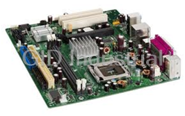
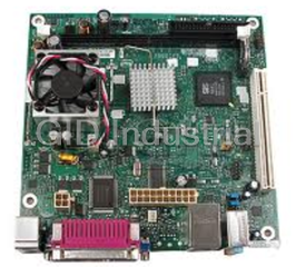
Intel D39287-002 CPU Cooler-Intel CPU Socket 604 Copper Cooler
Request a Quote

The quote request has been received
Close

Facing challenges or have inquiries? Feel free to contact us!
Call Us +1-469-283-2440
What they say about us
FANTASTIC RESOURCE
One of our top priorities is maintaining our business with precision, and we are constantly looking for affiliates that can help us achieve our goal. With the aid of GID Industrial, our obsolete product management has never been more efficient. They have been a great resource to our company, and have quickly become a go-to supplier on our list!
Bucher Emhart Glass
EXCELLENT SERVICE
With our strict fundamentals and high expectations, we were surprised when we came across GID Industrial and their competitive pricing. When we approached them with our issue, they were incredibly confident in being able to provide us with a seamless solution at the best price for us. GID Industrial quickly understood our needs and provided us with excellent service, as well as fully tested product to ensure what we received would be the right fit for our company.
Fuji
HARD TO FIND A BETTER PROVIDER
Our company provides services to aid in the manufacture of technological products, such as semiconductors and flat panel displays, and often searching for distributors of obsolete product we require can waste time and money. Finding GID Industrial proved to be a great asset to our company, with cost effective solutions and superior knowledge on all of their materials, it’d be hard to find a better provider of obsolete or hard to find products.
Applied Materials
CONSISTENTLY DELIVERS QUALITY SOLUTIONS
Over the years, the equipment used in our company becomes discontinued, but they’re still of great use to us and our customers. Once these products are no longer available through the manufacturer, finding a reliable, quick supplier is a necessity, and luckily for us, GID Industrial has provided the most trustworthy, quality solutions to our obsolete component needs.
Nidec Vamco
TERRIFIC RESOURCE
This company has been a terrific help to us (I work for Trican Well Service) in sourcing the Micron Ram Memory we needed for our Siemens computers. Great service! And great pricing! I know when the product is shipping and when it will arrive, all the way through the ordering process.
Trican Well Service
GO TO SOURCE
When I can't find an obsolete part, I first call GID and they'll come up with my parts every time. Great customer service and follow up as well. Scott emails me from time to time to touch base and see if we're having trouble finding something.....which is often with our 25 yr old equipment.
ConAgra Foods