

 Manufacturers
ICS ICS-110BL-32B
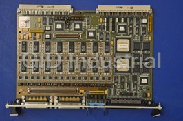
Description
ICS ICS-110BL-32B VME Bus Analog Input Board
Part Number
ICS-110BL-32B
Price
Request Quote
Manufacturer
ICS
Lead Time
Request Quote
Category
PRODUCTS - I
Specifications
Board Size
6U VMEbus Standard
Dynamic Range
> 110 dB in 128x oversampling mode, > 105 dB in 64x oversampling mode
FPDP Interface
Programmable Word Rate, up to 20Mwords/s
Full Scale Input
2.0 V pp differential*
Humidity
#95% Rel. Humidity, non-condensing
Input Impedance
10 kOhm
Input Sample Rate
128 X Output Rate for BW 22 kHz
Internal Sample Clock
Programmable in steps of 20 Hz (at output frequency)
Max. Input Signal BW
40 kHz
On-Board Storage
64 K Words
Operating Temp
0 to +50 Deg. C
Output Rate (Effective Sample Rate)
Max. 100 kHz/Ch., Min. 2 kHz/Ch
Output Word length
32 bits packed for 2 channels or 24 bits for, 1 channel on both VME or VSB , 24 bits only on FPDP
Power
6.0 Amps @ +5 V, 0.42 Amps @ +12 V, 0.25 Amps @ -12 V
Storage Temp
-40 to +85 Deg. C
VMEbus Interface
A32/24/16 D32 BLT Slave , Vectored Interrupts
VSBbus Interface
A32 D32 BLT Slave, Polled Interrupts
Features
- 24-bit sigma-delta A/D converters
- 64kword onboard storage
- External or internal clock and trigger
- Greater than 105 dB signal-to-noise ration (including harmonic distortion and crosstalk)
- Internal clock programmable in steps of less than 20 Hz at output frequency
- Optional 16-bit mode of operation
- Simultaneous sampling at rates up to 100 kHz/ch.
- Software selectable high pass filter for low frequency rejection
- Up to 32 differential input channels
- VME, VSB abd FPDP interfaces
Datasheet

Extracted Text
ICS-110BL 24-BIT DATA ACQUISITION BOARD No. 24, Rev. D Interactive Circuits & Systems Ltd. INTRODUCTION simultaneous sampling at high sample rates) in a single The ICS-110BL is designed to provide a complete data 20-slot VMEbus enclosure (see Figure 2). The ICS- acquisition solution in a single 6U VMEbus slot. The 110BL base board offers: ICS-110BL includes 32 24-bit, 100 kHz/channel sigma- delta ADCs, 64K FIFO buffer and VME, VSB and FPDP • up to 32 differential input channels; interfaces. It can accept an optional signal conditioning • 24-bit sigma-delta A/D converters; daughter card which offers 2-pole anti-alias filtering consistent with the anti-aliasing requirements of sigma- • simultaneous sampling at rates up to 100 kHz/ch.; delta ADCs, programmable gain of up to 31 dB in 0.5 dB • optional 16-bit mode of operation; steps, and internal test signal generation and injection capabilities. Designed for applications in sonar, digital • software selectable high pass filter for low frequency audio, vibration analysis, and test and measurement, the rejection; ICS-110BL board is a superior replacement for the • external or internal clock and trigger; company’s highly popular ICS-110A board. • internal clock programmable in steps of less than 20 The ICS-110BL combines the ultimate in analog and Hz at output frequency; digital technologies to offer unparalleled features and • greater than 105 dB signal-to noise ratio (including performance. The very high density of the ICS-110BL harmonic distortion and crosstalk); board allows users to implement a 576-channel signal conditioning and data acquisition system (with D 16 256K x 16 A PROM C INTERNAL TEST WAVEFORM SIGNAL SELECT 2-POLE TO MOTHER PROG. LOWPASS BOARD INPUT GAIN FILTER RELAY EXT. TEST DAUGHTER BOARD VME FPDP VME 24-BIT 64 KWORD INPUT ADC FIFO VSB MUX PROG. INT. EXT. MOTHER BOARD / EXT. CLK. CLK. K10391-0 Figure 1 - Simplified single-channel block diagram of the ICS-110BL with daughter board (model ICS-110BL) ICS-110B Sigma-Delta ADC Board • 64 Kword on-board storage; • high input impedance; • VME, VSB and FPDP interfaces for ADC data; • 2-pole low pass anti-alias filters; • front-panel sync bus for sample synchronization and • -95.0 dB to 31.5 dB programmable gain in steps of Front Panel Data Port (FPDP) bussing of up to 32 0.5 dB; boards. • internal or external test signal injection to all 32 channels by means of relays; The ICS-110BL, which contains the optional daughter card, features: • internal test signal stored in PROM (up to 8 16-bit signals of 32 K samples each). • up to 32 differential inputs; ICS - ICS - 7220- 110B1 110B1 ALU TO FOLLOWING FPDP SYSTEM 576 DIFF. ANALOG INPUTS { SYNCHRONIZING SIGNAL BUS ENSURES SYNC SIMULTANEOUS SAMPLING OF ALL CHANNELS FPDP ICS ICS ICS 18 x ICS-110B1 FPDP BUFFERING, AND FOR SIGNAL TEST SIGNAL ADDITION CONDITIONING & 24-BIT DATA ACQUISITION K10391A1 Figure 2 - A 576 channel signal conditioning and data acquisition system can now be included in a 20-slot VME enclosure using ICS-110BL boards Page 2 ICS-110B Sigma-Delta ADC Board SPECIFICATIONS ICS-110BL Mother Board No. of Diff. Analog Inputs: 8, 16 or 32 Input Impedance: 10 kOhm Full Scale Input: 2.0 V pp differential* Max. Input Signal BW: 40 kHz Input Sample Rate: 128 X Output Rate for BW < 22 kHz 64 X Output Rate for BW > 22 kHz Output Rate (Effective Sample Rate): Max. 100 kHz/Ch. Min. 2 kHz/Ch Internal Sample Clock: Programmable in steps of 20 Hz (at output frequency) Dynamic Range > 110 dB in 128x oversampling mode > 105 dB in 64x oversampling mode Total Harmonic Distortion: < -105 dB Crosstalk: < -105 dB On-Board Storage: 64 K Words Output Word length: 32 bits packed for 2 channels or 24 bits for 1 channel on both VME or VSB 24 bits only on FPDP VMEbus Interface: A32/24/16 D32 BLT Slave Vectored Interrupts VSBbus Interface: A32 D32 BLT Slave Polled Interrupts FPDP Interface: Refer to ICS Input Technical Note No. 15 Programmable Word Rate, up to 20Mwords/s Power: 6.0 Amps @ +5 V 0.42 Amps @ +12 V 0.25 Amps @ -12 V Operating Temp: 0 to +50 Deg. C Storage Temp: -40 to +85 Deg. C Humidity: #95% Rel. Humidity, non-condensing Board Size: 6U VMEbus Standard ICS-110BL Daughter Card No. Of Diff Inputs: 8, 16 or 32 Input Impedance: >1 M Ohm (with ±5 V max. input) >100 K Ohm (with ±25 V max. input) Max. Input Level: ±3.75V differential standard option (Contact factory for other options) Lowpass Filter: 2 - Pole Butterworth with a cut-off frequency of 75 kHz for a flat response up to 40kHz (Contact Factory for Other Options) Gain: -95.0 dB to +31.5 dB in steps of 0.5 dB Internal Test Signal: 8 16-bit preprogrammed waveforms in a 256K X 16 PROM Dynamic Range: >85 dB at 0 dB Gain and 2 Vpp Diff. Input Power: 0.34 Amps @ +5 V 0.29 Amps @ + 12 V 0.20 Amps @ -12 V Environmental: Same as ICS-110BL Mother Board * 2.0Vpp on each wire of differential pair. Specifications are subject to change without notice Page 3 ICS-110B Sigma-Delta ADC Board AK5393 also includes a digital highpass filter after the GENERAL DESCRIPTION decimator to remove low-frequency noise. The -3dB point is at 1.8 X Fs/48. In other words, the -3dB point of the MOTHER BOARD highpass filter’s response is at 3.6 Hz for Fs=96 kHz. The high pass filter can be disabled using a bit in the control Figure 3 shows a simplified block diagram of the register. The standard group delay through the AK5393 ICS-110BL baseboard. The board includes up to 32 FIR low pass filters is 34/Fo (all filters are linear phase). separate Sigma-Delta ADCs to simultaneously digitize all The group delay can be reduced to 10/Fo if the minimum channels at rates up to 100 KHz/ch. All inputs are phase filter option is selected. All of the converter’s differential to suppress common mode noise. The serial programmable features are available to the user. output from each ADC is converted to a 24-bit word before being stored in a FIFO for read-out. At the output, data is read as 32-bit words. Data from consecutive odd and even channels may be truncated to The ICS-110BL uses AKM’s AK5393 24-bit sigma-delta 16-bit resolution and packed together to form a 32-bit ADC converters. Each ADC converter samples the analog word for faster read-out from the VMEbus or VSB. Data input signal at 64 or 128 times the output rate (Fo). For may also be read-out in unpacked format as 24-bit words. Fo < 50 kHz, 128 x oversampling mode is recommended. The FPDP output, however, only supports unpacked For Fo > 50 kHz only 64 x oversampling mode can be format. A VMEbus or VSB interrupt can be generated at used. The sampling mode is set via the control register, FIFO half-full to facilitate real-time operation. which alters the decimation ratio of the digital filter. The maximum sample output frequency is 100 kHz. The P5 FPDP SYNC* DVALID* DATA STROBE 24 SUSPEND* NRDY* SYNC WORD FRONT-PANEL PROG. CLOCK INTERFACE ADC CH #0 SERIAL TO ADC PARALLEL 16 CH #2 32K word AND FIFO 16:1 MUX . . . . (EVEN) . . . . W CH #30 ADC 32 ADC CH #1 SERIAL TO PARALLEL 16 ADC CH #3 32K word AND FIFO 16:1 MUX (ODD) . . . . 32 32 W . . . . FIFO CH #31 ADC HALF-FULL VMEbus VMEbus INTERFACE INTERFACE FSI CLK SYNC WORD 32 32 INTERRUPT CLK CONTROL PROG. VMEbus VSBbus FRAME_SYNC LOGIC CLOCK ACQUIRE_SYNC EXT. ACQ. K10391A3.CFL VMEbus P4 LOCAL BUS Figure 3 - ICS-110BL Mother Board Block Diagram Page 4 . ICS-110B Sigma- Delta ADC Board The ICS-110BL can use either an external clock or the all 32-signal conditioning and ADC stages. The board’s internal clock as the sampling clock. The required test signal input is signal is single-ended. The clock frequency is 256 times the output data rate. The internal test signal is generated from a internal clock can be programmed to produce a sampling preprogrammed PROM, which can hold as many rate with excellent accuracy (usually to within 40ppm) by as 8 waveforms up to 32K samples each. The writing the appropriate clock frequency word to the PROM is operated in a loop address mode in board’s PROGRAM_CLOCK register. The minimum Fo order to generate a periodic signal. The standard is 2 kHz. The board includes a programmable decimator, option for test signals include: single-tone; dual- which simply rejects output samples to reduce Fo by a tone; pseudo-noise; etc. A 16-bit filtered delta- factor of up to 16. Note, however, that the antialising sigma DAC is used to produce an analog signal. characteristics of the sigma-delta converters are lost when The switching between the actual input signals, this feature is selected. Hence, this mode should only be external test signal and internal test signal is selected when using a Fo of less than 2kHz. done under software control. The acquisition period can be controlled either from the Other signal conditioning daughter cards are being VMEbus (through software control), or by applying an planned for different applications. Please contact the external signal conforming to differential TTL signal factory for details. levels to the EXTERNAL_ACQUIRE input. A high level signal causes acquisition to occur, while a low level DETAILED DESCRIPTION signal causes acquisition to stop. Acquisition is automatically synchronized so that a full frame of data is DAUGHTER BOARD always written to the FIFO at the beginning or end of an acquisition cycle. Figure 4 shows a simplified block diagram of the signal conditioning daughter card for the ICS-110BL board. It The ICS-110BL includes a very powerful FPDP interface, includes, for each channel, a differential receiver, which which allows up to 32 ICS-110BL boards to be bussed. offers high input impedance. A resistive divider stage is To synchronize multiple ICS-110BL boards, one board included at the input to allow an over voltage capability. The must be configured as “master” in order to supply input impedance is dependent on the maximum voltage synchronization signals to the other slave boards. These input requirement. signals are available at the front-panel P4 local bus connector. The signal conditioning circuit also includes a 2-pole low pass filter with a fixed cut-off frequency and a gain stage DAUGHTER CARD which offers programmable gain from -95.0 dB to 31.5 dB in steps of 0.5 dB. The ICS-110BL base board includes a provision for a daughter card for signal conditioning. Figure 4 provides a For off-line test, an internal or an external test signal can be simplified block diagram of the daughter card version injected into the signal path following the differential (ICS-110BL), which includes the following: receiver stage. The internal test signal is factory programmed in to a 256K x 16 EPROM. The user can select • A 2-pole low-pass filter with a fixed cut-off one of any 8 pre-stored signals. A 16-bit delta-sigma DAC is frequency of 75 kHz in order to ensure a flat used for digital-to-analog conversion. The typical dynamic passband response extending up to 40 kHz. range is around 90 dB. Note that high-reliability electro- Typically, no more than a 2-pole filter is mechanical relays are used to switch between required for anti-aliasing because of the high internal/external test signals or actual signals. All channels input sampling rate inherent in a sigma-delta receive the same test signals. ADC converter. An alternate filter cut-off frequency may be offered. Contact factory for details. • A programmable attenuation/gain stage which offers -95.0 dB to +31.5 dB attenuation/gain in steps of 0.5 dB. • An internal or external test signal injection capability that allows injection of a test signal to Page 5 ICS-110B Sigma-Delta ADC Board EPROM EXT. WAVE TEST DAC TABLE SIGNAL 16 RELAY INT./EXT. TEST GAIN RI TO FROM + MOTHER ICS-110B BOARD INPUT - INPUTS CONNECTOR RELAY DIFF. RI RECEIVER 8 2-POLE LOWPASS FILTER R2 R2 VME K10391-2 Figure 4 - Signal Conditioning Daughter Card (Single Channel Shown) MOTHER BOARD The AK5393 uses a 7th order tri-level delta-sigma modulator to sample the analog input signal at either 128 or Sigma-Delta Analog Conversion 64 times the output sample rate of the device. The result of such high rate sampling of the input signal is that the The operation of a Sigma-Delta ADC differs significantly Nyquist frequency is moved to at least 6 octaves (for 64 from traditional ADCs. A simple 1-bit analog-to-digital times oversampling) or 7 octaves (for 128 times conversion is performed at a very high rate. The total oversampling) away from the highest signal frequency. The quantization noise energy remains constant, but by anti-aliasing requirement is, therefore, drastically reduced. spreading it over a wider spectrum, the amount in the frequency band of interest is reduced. The noise in the Since the input differential amplifier for each channel of the passband is further reduced by filtering (noise shaping). The ICS-110BL board has a finite bandwidth, no more than a 2- oversampled signal is then lowpass filtered to remove the out-of-band quantization noise. This is achieved using two pole filter is required for anti-aliasing. The signal digital filters: a decimating comb filter and an FIR low-pass conditioning daughter card of the ICS-110BL board filter/decimator. The resultant output spectrum is equivalent includes a filter of this type. to a traditional ADC. 10K +1V 10K - + -1V - ve + INPUT SIGNAL + 1.25v TO ADC INPUT + +1V + ve - - -1V 10K 10K K10166-2 Figure 5 - ICS-110BL Analog Input Configuration Page 6 . ICS-110B Sigma- Delta ADC Board Input Section Sampling Clock The ICS-110BL board accepts true differential input signals; The ICS-110BL board can be configured (by programming peak amplitudes of ± 1.0V on each input, as shown in Figure the control register) for internal or external sampling. The 5, produce a full-scale output. The input impedance is 10K external CLOCK input is TTL differential. A single-ended ohm. The maximum input signal bandwidth is 40 kHz. TTL clock signal can also be used provided that the high logic level is above 3.5 volts. This CLOCK input frequency For best performance, differential input signals are must be 256 times the desired output. recommended. If, however, single-ended inputs must be used, the -ve input terminals can be tied to a common analog As mentioned above, the sampling clock can also be sourced ground, preferably the ground of the source. The input from an internal programmable clock oscillator, which has a signal is applied to the +ve terminal. The full-scale swing of resolution of less than 20 Hz at the sample output frequency. the input signal should not exceed ± 1.0V. Thus, for single ended input, there is a 6 dB loss in dynamic range. The internal clock (after conversion to differential TTL signals) is available at the P4 front-panel connector pins in Dynamic Range order to supply clock signals to other ICS-110B boards for synchronous operation. The board generating the clock The ICS-110BL typically offers 110 dB S/N ratios in the signal (master board) requires appropriate jumper settings in 128 times oversampling mode. The S/N ratio is order to route the clock signals back to the P4 connector. approximately 105 dB in the 64 times oversampling mode. All slave ICS-110BL boards must be configured for external The total harmonic distortion is typically -105 dB. A typical clock. Thus all boards including the master see identical 1024-point FFT plot of the ADC output is shown in Figure propagation delays for the clock signal, regardless of 6(a). The input is a synthesized single tone (differential) and whether it is generated by an ICS-110BL board or applied the output rate is 100 kHz/channel. The crosstalk from an external source. The maximum clock frequency is performance of a typical channel (input shorted) while all 25.6 MHz and the minimum clock frequency is 512 kHz. other channels are driven by a 20 kHz tone is illustrated in Figure 6(b). Note that all spurious components lie below - Output Decimation 110 dB with respect to the ADC full-scale output. The output rate can be reduced using decimation. At the The ICS-110BL offers excellent gain and phase matching output, samples are automatically discarded, which has the across channels. Since the Sigma-Delta converters employ effect of lowering the effective sampling rate. The minimal analog technologies, such performance is expected. decimation factor can be as high as 16. In the design of the ICS-110BL board, extreme care has been The user is cautioned that decimating the output requires Taken in the generation of sampling clocks in order to anti-aliasing (similar to using a conventional ADC) in order assure precise simultaneous sampling on every card, and to bandlimit the input signal to the Nyquist frequency, which across cards in a multi-board system. is equal to half the final output rate. Thus, output decimation is only recommended for reducing the output The frequency response is flat over the entire signal rate below 2 kHz. bandwidth (45% of the output rate). Page 7 ICS-110B Sigma-Delta ADC Board 0 -20 -40 -60 -80 -100 -120 -140 -160 100 200 300 400 500 600 700 800 900 1000 Frequency [bin] Figure 6(a) - 2048-point FFT in 24-bit mode at 100 kHz 0 -20 -40 -60 -80 -100 -120 -140 -160 100 200 300 400 500 600 700 800 900 1000 Frequency [bin] Figure 6(b) - Crosstalk Performance with 20 kHz Tone on all Other Channels Page 8 Amplitude [dB] Amplitude [dB] . ICS-110B Sigma- Delta ADC Board DATA_CLOCK FPDP_DATA 01 2 31 33 34 62 30 32 63 BUS_IDLE MASTER DRIVES BUS SLAVE WITH BOARD_ADDRESS=1 DRIVES BUS BUS_IDLE DATA_STROBE /SYNC MASTER ALWAYS DRIVES DATA_STROBE & /SYNC K10187- Figure 7 - FPDP Timing with Multiple Boards Acquisition Trigger Front Panel Interface The triggering of acquisition can be done either internally, by writing to the control register, or externally, by applying The ICS-110BL includes a Front Panel Data Port (FPDP) a signal to the EXTERNAL_ACQUIRE input. In either for high-speed data transfer. The FPDP protocol for data case, the effect is to start and stop acquisition by inhibiting transfer is supported by all ICS products, including the ICS- FIFO writes; the ADCs are always converting data. The 2200 DSP board, the ICS-7220 General Purpose I/O board, operation is frame-oriented: acquisition can only be started and the ICS-115 Analog Output board. An 80-pin at the beginning of a frame and stopped at the end of a connector (KEL 8831-080-170L) is provided for the FPDP. frame; a frame is defined as a set of sampled data for all Refer to INPUT Technical Note No.15 for more details. selected channels for one sample instant. The number of channels included in the frame is programmable, but always The ICS-110BL FPDP may be bussed between multiple ICS-110BL boards for systems requiring more than 32 starts from channel 1 and runs consecutively up to the channels of analog input. The first board of a cluster must number of channels selected. Only even numbers of be configured as the master, by means of wire links on the channels may be selected. board. The master generates the FPDP Strobe, Data Valid and Sync signals and terminates various bus signals. It For external control of acquisition start/stop, the differential also generates signals on the P4 local bus, which control EXTERNAL_ACQUIRE input must be used. A TTL high the timing for the slave boards so that each board drives its data onto the bus in the correct time period. This level starts acquisition and the acquisition stops when the feature, combined with the multiple board signal is dropped to a TTL low level. Bringing the signal synchronization capability of the ICS-110BL described back to a TTL high level can restart the acquisition. Here elsewhere in this note, allows the user to construct large again, a single-ended TTL signal can be used provided the data acquisition systems of up to 1,024 channels with high logic level is above 3.5 volts. simultaneous sampling across all channels and a single FPDP cable passing data to one or more FPDP receive SYNC Word interfaces. Figure 7 illustrates the timing relationship of the FPDP data When reading data from the 32-bit VMEbus or VSB and control signals for a 2 board 64-channel system. The interface, a user-programmable 32-bit sync word can be FPDP Data Strobe (clock) rate is software programmable, used to maintain synchronization. This optional with a maximum frequency of 20 MHz. Two types of Data SYNC_WORD Strobe signal are available: the TTL level STROB and the is automatically written to the ADC_DATA FIFO at the positive-logic ECL differential clocks (PSTROBE+ & beginning of every frame. The SYNC_WORD option is not PSTROBE-). The latter signals support longer cable lengths available on the front panel data port. and higher speed operation, and provide better noise immunity. The ICS-110BL supports only the unpacked 24- bit data width on the FPDP port. Page 9 ICS-110B Sigma-Delta ADC Board The Front Panel Data Port operates using two FIFO VSB Interface memories in a swing buffer configuration, as shown in Figure 8. During one frame, data is converted and written to The ICS-110BL also includes a Slave A32/D32 VSB one FIFO memory, while data is being read from the other interface. The VSB interface supports block transfers, as over the FPDP. At the end of the frame, the two banks well as polled interrupts. Data rates up to 40 MBytes/sec are switch. Before any new ADC data is written to the swapped achievable. Data organization is as discussed in the FIFO memory, it is automatically reset to ensure channel VMEbus Interface section. synchronization. In the unlikely event that the synchronization is lost, the scheme ensures that it is Multiple-Board Synchronization recovered in the next frame. An important design feature of the ICS-110BL card is its ability to be integrated into a multi-board system in perfect By programming the FPDP_BLOCK_COUNT register, the synchronism using no additional hardware and no additional user can set the bank switch to occur after storing a user- design effort. This section discusses in some detail the P4 programmable number of frames. Local Bus signals used to achieve synchronism in a multi- board system. The interface requires only the bussing of the VMEbus Interface master ICS-110BL P4 Local Bus connector to one or more slave cards, and the initialization of a few registers on the The ICS-110BL is supported by a Slave A32/D32 VMEbus master. interface. The VMEbus interface supports D32 block transfers and vectored interrupts. Data rates up to 32 To ensure sampling synchronization from board to board in MBytes/sec are achievable. a multiple board configuration, three synchronization signals are driven by the master ICS-110BL and decoded by all Although data is always accessed using 32-bit data transfers, boards across the P4 Local Bus connector. To keep channel data can be organized as two channels per transfer sampling skew to a minimum, all SYNC signals are (packed format) or one channel per transfer (unpacked generated and then received locally by the master, so that the format). In packed format, the data is truncated to 16 bits master sees the same gate delays and decoding logic as seen and ordered so that channel N is in the upper 16 bits, and by the slave cards. In effect, the master is its own slave. channel N+1 is in the lower 16 bits of the 32-bit data word. In unpacked format, the channel data is located in the upper 24 bits of the 32-bit data word; the lower 8 bits are forced to zero. STROBE (TTL or PECL DIFF.) DATA VALID SYNC FPDP SUSPEND I/F DATA 16 CH#1 ADC FIFO SERIAL TO PARALLEL AND MUX FIFO CH#32 ADC K10184-5 Figure 8 - ICS-110BL FPDP Configuration Page 10 . ICS-110B Sigma- Delta ADC Board CLOCK FRAME_SYNC SAMPLING INSTANTS SYNC UP LOCAL ADC CLOCK K10184A2 Figure 9 - Master/Slave CLOCK Phase Synchronization FRAME_SYNC Register Descriptions The FRAME_SYNC signal is used to synchronize all boards with respect to the sampling clock. This signal is The NUM_CHANS register must be programmed to specify received. the number of channels to be used on the board. The By each slave board and used to re-synchronize the NUM_CHANS_FPDP register allows the user to select the converters at the next rising edge of the oversampling clock, total number of channels when using the FPDP for output as shown in Figure 9 with multiple ICS-110BL boards; it only needs to be programmed on the master board. The number of channels ACQUIRE_SYNC in either case must be an even number, and, in a multiple The ICS-110BL is capable of decimating the Sigma-Delta board configuration, all boards except the last must be 32- output by a user-defined number of frames. The channel boards and must have a full complement of ACQUIRE_SYNC signal simply ensures that both the channels selected. master and its slaves decimate the same frames by informing the slaves who converted data frame is to be stored to the For example, an 80-channel system would consist of three ADC_DATA FIFO. Decimated frames are simply rejected boards defined as follows: and not written to the ADC_DATA FIFO. Master: NUM_CHANS=31 (32 channels) Memory Map NUM_CHANS_FPDP=79 (80 channels) The ICS-110BL memory map is shown in Figures 10, 11 Middle Slave: NUM_CHANS=31 (32 channels) and 12. Figure 10 shows a summary of the map, while Figures 11 and 12 show the bit allocation within registers. End Slave: NUM_CHANS=15 (16 channels) The control register allows the user to configure the following operating parameters: The maximum number of channels in a multiple board • Acquisition start and stop control system when using the front panel data port is limited to 1,024, i.e. 32 boards (NUM_CHANS_FPDP=1023). • Master/slave (multiple board) selection • Acquisition source (internal/external) The DECIMATION register allows the user to specify the • Output mode (VMEbus, VSB, FPDP) decimation factor in the range 1 to 16. The FPDP • Sync word enable/disable ADDRESS register specifies the board address in a multiple • Clock source (internal/external) board system when using FPDP. • VSB interrupt enable/disable • VMEbus interrupt enable/disable Page 11 ICS-110B Sigma-Delta ADC Board VMEbus D15 D0 D31 BASE + 0x0 ADC DATA STATUS/RESET BASE + 0xFE00 CONTROL BASE + 0xFE02 INT. VECTOR BASE + 0xFE04 NUM CHANS BASE + 0xFE06 DECIMATION BASE + 0xFE08 ADC CONFIGURATION BASE + 0xFE0A CALIBRATION BASE + 0xFE0C FPDP ADDRESS BASE + 0xFE0E NUM CHANS FPDP BASE + 0xFE10 FPDP BLOCK COUNT BASE + 0xFE12 VSB BASE ADDRESS BASE + 0xFE14 VSB SPACE CODE BASE + 0xFE16 SYNC WORD BASE + 0xFE18 CLOCK FREQUENCY BASE + 0xFE1C VSBbus D31 D0 BASE + 0x0 ADC_DATA BASE + 0x8000 VSB STATUS INTERRUPT ENABLE BASE + 0xC000 K10373-0 Figure 10 - ICS-110BL Memory Map Page 12 . ICS-110B Sigma- Delta ADC Board D8 D7 D3 D2 D1 D0 BOARD FIFO ACQUIRE /FIFO /FIFO /FIFO RESET RESET ENABLED FULL HALF- EMPTY FULL BASE + 0xFE00 READ/WRITE STATUS/RESET D15 D14 D8 D7 D6 D5 D4 D3 D2 D1 D0 OVER- VME_INT VSB_INT CLOCK SYNC ACQUIRE MASTER ACQUIRE OUTPUT MODE SAMPLING ENABLE ENABLE SEL ENABLE SOURCE RATIO BASE + 0xFE02 READ/WRITE CONTROL D7 D6 D5 D4 D3 D2 D1 D0 INTERRUPT_VECTOR BASE + 0xFE04 READ/WRITE INTERRUPT_VECTOR D3 D2 D1 D0 NUM_CHANNELS BASE + 0xFE06 WRITE ONLY NUM_CHANNELS D4 D3 D2 D1 D0 DECIMATION BASE + 0xFE08 WRITE ONLY DECIMATION D7 D6 D5 D4 D3 D2 D1 D0 CHIP ADC_CONFIGURATION SEL BASE + 0xFE0A WRITE ONLY ADC_CONFIGURATION D7 D6 D2 D1 D0 CLOCK CAL CAL CAL CAL SEL ENABLE SEL SEL SEL 2 1 0 BASE + 0xFE0C READ/WRITE ADC_CALIBRATION D4 D3 D2 D1 D0 FPDP_ADDRESS BASE + FE0E WRITE ONLY FPDP_ADDRESS D9 D8 D7 D6 D5 D4 D3 D2 D1 D0 NUM_CHANNELS_FPDP BASE + FE10 WRITE ONLY NUM_CHANNELS_FPDP K10373A1 Figure 11 - ICS-110BL Register Description Page 13 ICS-110B Sigma-Delta ADC Board D7 D6 D5 D4 D3 D2 D1 D0 FPDP_BLOCK_COUNT BASE + 0xFE12 WRITE ONLY FPDP_BLOCK_COUNT D15 D14 D7 D6 D5 D4 D3 D2 D1 D0 VSB_BASE_ADDR BASE + 0xFE14 WRITE ONLY VSB_BASE_ADDR D1 D0 VSB_SPACE_CODE BASE + 0xFE16 WRITE ONLY VSB_SPACE_CODE D31 D30 D7 D6 D5 D4 D3 D2 D1 D0 SYNC_WORD BASE + 0xFE18 WRITE ONLY SYNC_WORD D23 D21 D20 D19 D4D3D2D1D0 DEST. CLOCK_FREQUENCY BASE + 0xFE1C WRITE ONLY CLOCK_FREQUENCY D31 D30 D29 D28 D26 D25 D24 /FIFO VSB /FIFO HALF- /FIFO GLOBAL ADDRESS INT. FULL FULL EMPTY BASE + 0x8000 READ ONLY VSB_STATUS K10373A2 Figure 12 - ICS-110BL Register Descriptions (cont’d) Page 14 . ICS-110B Sigma- Delta ADC Board SOFTWARE DEVICE DRIVERS A comprehensive software device driver for the VxWorks to use the library in preference to direct use of the real-time operating system supports the ICS-110BL. The device driver interface, since this will reduce the driver includes the following elements: need to understand the details of board operation and will speed up integration. • A device driver conforming to the VxWorks model, including support for Open, Close, Read, Write and • Driver and library source code. For users who wish IOCTL functions, and device initialization and to port the driver to their own operating system, attachment. complete ‘C’ language source code is provided. • A comprehensive library of high-level functions, The following are examples of some of the library routines. Each function carries a list of parameters that are which may be included with the application not described here: programmer’s code. They provide control of all aspects of the ICS-110BL. Programmers are advised ics110blSampleRateSet() Sets the sampling frequency. ics110blVmeInterruptWait() Waits for interrupt or timeout to occur ics110blDeviceReset() Resets ICS-110BL to initial conditions ics110blMasterSet() Sets board as sampling master (for multiple board configurations) ics110blAcqSrcSet() Sets acquisition trigger as internal or external int ics110blOutputModeSet() Sets the output path as VMEbus, VSB or FPDP ics110blOversamplingSet() Sets the converter oversampling ratio ics110blDecimationSet() Set decimation ratio ics110blIntVectorSet() Load VMEbus interrupt vector ics110blVsbBaseAddressSet() Load VSB base address ics110blStatusRead() Read board status ics110blFifoRead() Read sample data ics110blSampleRateSet() Set frequency of onboard sampling clock ics110blProgramAdc() Set converter characteristics such as software initiated calibration, FIR filter coefficients ics110blCalibrateAdc() Calibrate ICS-110BL converters ics110blGainSet() Set signal conditioner gain ics110blAcquireSet() Start conversion INPUT is published by ICS Ltd. and is available free of charge. Your input is welcome; please call or write to ICS.
Frequently asked questions
What makes Elite.Parts unique?

What kind of warranty will the ICS-110BL-32B have?
Which carriers does Elite.Parts work with?
Will Elite.Parts sell to me even though I live outside the USA?
I have a preferred payment method. Will Elite.Parts accept it?
Why buy from GID?

Quality
We are industry veterans who take pride in our work

Protection
Avoid the dangers of risky trading in the gray market

Access
Our network of suppliers is ready and at your disposal

Savings
Maintain legacy systems to prevent costly downtime

Speed
Time is of the essence, and we are respectful of yours
Related Products

ICS ICS9250BF-27 Frequency Generator and Integrated Buffers for Celeron & PII/III
Request a Quote

The quote request has been received
Close

Facing challenges or have inquiries? Feel free to contact us!
Call Us +1-469-283-2440
What they say about us
FANTASTIC RESOURCE
One of our top priorities is maintaining our business with precision, and we are constantly looking for affiliates that can help us achieve our goal. With the aid of GID Industrial, our obsolete product management has never been more efficient. They have been a great resource to our company, and have quickly become a go-to supplier on our list!
Bucher Emhart Glass
EXCELLENT SERVICE
With our strict fundamentals and high expectations, we were surprised when we came across GID Industrial and their competitive pricing. When we approached them with our issue, they were incredibly confident in being able to provide us with a seamless solution at the best price for us. GID Industrial quickly understood our needs and provided us with excellent service, as well as fully tested product to ensure what we received would be the right fit for our company.
Fuji
HARD TO FIND A BETTER PROVIDER
Our company provides services to aid in the manufacture of technological products, such as semiconductors and flat panel displays, and often searching for distributors of obsolete product we require can waste time and money. Finding GID Industrial proved to be a great asset to our company, with cost effective solutions and superior knowledge on all of their materials, it’d be hard to find a better provider of obsolete or hard to find products.
Applied Materials
CONSISTENTLY DELIVERS QUALITY SOLUTIONS
Over the years, the equipment used in our company becomes discontinued, but they’re still of great use to us and our customers. Once these products are no longer available through the manufacturer, finding a reliable, quick supplier is a necessity, and luckily for us, GID Industrial has provided the most trustworthy, quality solutions to our obsolete component needs.
Nidec Vamco
TERRIFIC RESOURCE
This company has been a terrific help to us (I work for Trican Well Service) in sourcing the Micron Ram Memory we needed for our Siemens computers. Great service! And great pricing! I know when the product is shipping and when it will arrive, all the way through the ordering process.
Trican Well Service
GO TO SOURCE
When I can't find an obsolete part, I first call GID and they'll come up with my parts every time. Great customer service and follow up as well. Scott emails me from time to time to touch base and see if we're having trouble finding something.....which is often with our 25 yr old equipment.
ConAgra Foods