

 Manufacturers
GENERAL ELECTRIC VME-1182
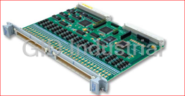
Description
VME Form Factor, Opto-isolated front I/O Interface, 64Channels, 0º to +55º Temp (C), Forced Air Conduction Cooling
Part Number
VME-1182
Price
Request Quote
Manufacturer
GENERAL ELECTRIC
Lead Time
Request Quote
Category
PRODUCTS - V
Features
- 1500VDC or 1100VRMS channel-to-channel and channel-to-VME isolation (1
- 64 optically isolated inputs
- A24/A16 addressing capability
- Available in 5 to 250VDC or 4 to 240VAC options
- Available in contact sensing or voltage sensing options
- COS monitoring software controlled on a channel-by-channel basis
- Debounce time software controlled on a channel-by-channel basis
- minute)
- Multiple-functions available per channel
- Programmable debounce times
- Pulse accumulation for up to 65,535 pulses per channel
- Pulse accumulation reporting
- Release-On-Acknowledge (ROAK) interrupts on all VME levels
- SOE monitoring on a channel-by-channel basis
- SOE reporting
- Supervisory bus access, nonprivileged bus access, or both
- Time tag reporting
Datasheet

Extracted Text
GE Fanuc Automation VME-1182 64-Channel Isolated Digital Input Board with Multifunctional Intelligent Controller PRODUCT MANUAL 500-001182-000 REV E This page is intentionally left blank. COPYRIGHT AND TRADEMARKS The information in this document has been carefully checked and is believed to be entirely reliable. While all reasonable efforts to ensure accuracy have been taken in the preparation of this manual, GE Fanuc Embedded Systems assumes no responsibility resulting from omissions or errors in this manual, or from the use of information contained herein. GE Fanuc Embedded Systems reserves the right to make any changes, without notice, to this or any of GE Fanuc Embedded Systems’ products to improve reliability, performance, function, or design. GE Fanuc Embedded Systems does not assume any liability arising out of the application or use of any product or circuit described herein; nor does GE Fanuc Embedded Systems convey any license under its patent rights or the rights of others. For warranty and repair policies, refer to GE Fanuc Embedded Systems’ Standard Conditions of Sale. AMXbus, BITMODULE, COSMODULE, DMAbus, IOMax, IOWorks Access, IOWorks Foundation, IOWorks Manager, IOWorks Server, MAGICWARE, MEGAMODULE, PLC ACCELERATOR (ACCELERATION), Quick Link, RTnet, Soft Logic Link, SRTbus, TESTCAL, “The Next Generation PLC”, The PLC Connection, TURBOMODULE, UCLIO, UIOD, UPLC, Visual Soft Logic Control(ler), VMEbus Access, VMEmanager, VMEmonitor, VMEnet, VMEnet II, VMEprobe and VMIC Shutdown are trademarks and The I/O Experts, The I/O Systems Experts, The Soft Logic Experts, and The Total Solutions Provider are service marks of GE Fanuc Embedded Systems. IOWorks, Visual IOWorks and the VMIC logo are registered trademarks of GE Fanuc Embedded Systems. Other registered trademarks are the property of their respective owners. Copyright © 2007 by GE Fanuc Embedded Systems. All Rights Reserved. This document shall not be duplicated, nor its contents used for any purpose, unless granted express written permission from GE Fanuc Embedded Systems. This page is intentionally left blank. Table of Contents List of Figures . . . . . . . . . . . . . . . . . . . . . . . . . . . . . . . . . . . . . . . . . . . . . . . . . . . . . . . . . . . . . . . . . . . 7 List of Tables . . . . . . . . . . . . . . . . . . . . . . . . . . . . . . . . . . . . . . . . . . . . . . . . . . . . . . . . . . . . . . . . . . . . 9 Overview . . . . . . . . . . . . . . . . . . . . . . . . . . . . . . . . . . . . . . . . . . . . . . . . . . . . . . . . . . . . . . . . . . . . . . . 11 Features. . . . . . . . . . . . . . . . . . . . . . . . . . . . . . . . . . . . . . . . . . . . . . . . . . . . . . . . . . . . . . . . . . . . 11 Functional Description . . . . . . . . . . . . . . . . . . . . . . . . . . . . . . . . . . . . . . . . . . . . . . . . . . . . . . . . . . . . 12 References . . . . . . . . . . . . . . . . . . . . . . . . . . . . . . . . . . . . . . . . . . . . . . . . . . . . . . . . . . . . . . . . . . . . . 13 Safety Summary . . . . . . . . . . . . . . . . . . . . . . . . . . . . . . . . . . . . . . . . . . . . . . . . . . . . . . . . . . . . . . . . . 15 Warnings, Cautions and Notes. . . . . . . . . . . . . . . . . . . . . . . . . . . . . . . . . . . . . . . . . . . . . . . . . . . . . . 16 Chapter 1 - Theory of Operation . . . . . . . . . . . . . . . . . . . . . . . . . . . . . . . . . . . . . . . . . . . . . . . . . 17 Internal Functional Organization . . . . . . . . . . . . . . . . . . . . . . . . . . . . . . . . . . . . . . . . . . . . . . . . . 17 Field Inputs . . . . . . . . . . . . . . . . . . . . . . . . . . . . . . . . . . . . . . . . . . . . . . . . . . . . . . . . . . . . . . . . . . . . . 19 Voltage Sensing. . . . . . . . . . . . . . . . . . . . . . . . . . . . . . . . . . . . . . . . . . . . . . . . . . . . . . . . . . . . . . 19 Contact Sensing. . . . . . . . . . . . . . . . . . . . . . . . . . . . . . . . . . . . . . . . . . . . . . . . . . . . . . . . . . . . . . 19 Input Data Processing . . . . . . . . . . . . . . . . . . . . . . . . . . . . . . . . . . . . . . . . . . . . . . . . . . . . . . . . . . . . 20 Debounce Time . . . . . . . . . . . . . . . . . . . . . . . . . . . . . . . . . . . . . . . . . . . . . . . . . . . . . . . . . . . . . . 20 Pulse Accumulation . . . . . . . . . . . . . . . . . . . . . . . . . . . . . . . . . . . . . . . . . . . . . . . . . . . . . . . . . . . 20 COS Definition . . . . . . . . . . . . . . . . . . . . . . . . . . . . . . . . . . . . . . . . . . . . . . . . . . . . . . . . . . . . . . . 20 Time Tag Clock . . . . . . . . . . . . . . . . . . . . . . . . . . . . . . . . . . . . . . . . . . . . . . . . . . . . . . . . . . . . . . 21 Sequence of Event. . . . . . . . . . . . . . . . . . . . . . . . . . . . . . . . . . . . . . . . . . . . . . . . . . . . . . . . . . . . 21 EPROM . . . . . . . . . . . . . . . . . . . . . . . . . . . . . . . . . . . . . . . . . . . . . . . . . . . . . . . . . . . . . . . . . . . . 21 VME Interface. . . . . . . . . . . . . . . . . . . . . . . . . . . . . . . . . . . . . . . . . . . . . . . . . . . . . . . . . . . . . . . . . . . 22 Control Logic . . . . . . . . . . . . . . . . . . . . . . . . . . . . . . . . . . . . . . . . . . . . . . . . . . . . . . . . . . . . . . . . 22 Bus Interrupter . . . . . . . . . . . . . . . . . . . . . . . . . . . . . . . . . . . . . . . . . . . . . . . . . . . . . . . . . . . . . . . . . . 23 Watchdog Timer . . . . . . . . . . . . . . . . . . . . . . . . . . . . . . . . . . . . . . . . . . . . . . . . . . . . . . . . . . . . . . . . . 24 Self-Test . . . . . . . . . . . . . . . . . . . . . . . . . . . . . . . . . . . . . . . . . . . . . . . . . . . . . . . . . . . . . . . . . . . . . . . 25 Power Requirements . . . . . . . . . . . . . . . . . . . . . . . . . . . . . . . . . . . . . . . . . . . . . . . . . . . . . . . . . . . . . 26 5 VMIVME-1182 64-Channel Isolated Digital Input Board with Multifunctional Intelligent Controller Chapter 2 - Configuration and Installation . . . . . . . . . . . . . . . . . . . . . . . . . . . . . . . . . . . . . . .27 Unpacking Procedures . . . . . . . . . . . . . . . . . . . . . . . . . . . . . . . . . . . . . . . . . . . . . . . . . . . . . . . . . . . 28 Physical Installation . . . . . . . . . . . . . . . . . . . . . . . . . . . . . . . . . . . . . . . . . . . . . . . . . . . . . . . . . . . . . . 29 Operational Configuration . . . . . . . . . . . . . . . . . . . . . . . . . . . . . . . . . . . . . . . . . . . . . . . . . . . . . . . . . 30 Factory-Installed Jumpers. . . . . . . . . . . . . . . . . . . . . . . . . . . . . . . . . . . . . . . . . . . . . . . . . . . . . . 30 Access Modes. . . . . . . . . . . . . . . . . . . . . . . . . . . . . . . . . . . . . . . . . . . . . . . . . . . . . . . . . . . . . . . 32 Address Modes . . . . . . . . . . . . . . . . . . . . . . . . . . . . . . . . . . . . . . . . . . . . . . . . . . . . . . . . . . . . . . 32 Board Address . . . . . . . . . . . . . . . . . . . . . . . . . . . . . . . . . . . . . . . . . . . . . . . . . . . . . . . . . . . . . . 32 Field Input Configurations . . . . . . . . . . . . . . . . . . . . . . . . . . . . . . . . . . . . . . . . . . . . . . . . . . . . . . . . . 34 Voltage Sensing . . . . . . . . . . . . . . . . . . . . . . . . . . . . . . . . . . . . . . . . . . . . . . . . . . . . . . . . . . . . . 34 Contact Sensing - Wetting Voltage at P2 . . . . . . . . . . . . . . . . . . . . . . . . . . . . . . . . . . . . . . . . . . 35 Contact Sensing - Wetting Voltage at P3 . . . . . . . . . . . . . . . . . . . . . . . . . . . . . . . . . . . . . . . . . . 36 System Connections . . . . . . . . . . . . . . . . . . . . . . . . . . . . . . . . . . . . . . . . . . . . . . . . . . . . . . . . . . . . . 38 Chapter 3 - Programming . . . . . . . . . . . . . . . . . . . . . . . . . . . . . . . . . . . . . . . . . . . . . . . . . . . . . . . .41 Board ID Register (BID). . . . . . . . . . . . . . . . . . . . . . . . . . . . . . . . . . . . . . . . . . . . . . . . . . . . . . . . . . . 43 Control and Status Register (CSR) . . . . . . . . . . . . . . . . . . . . . . . . . . . . . . . . . . . . . . . . . . . . . . . . . . 44 Self-Test Results Register (STR) . . . . . . . . . . . . . . . . . . . . . . . . . . . . . . . . . . . . . . . . . . . . . . . . . . . 46 Interrupt Vector Register (IVR) . . . . . . . . . . . . . . . . . . . . . . . . . . . . . . . . . . . . . . . . . . . . . . . . . . . . . 47 Debounced Input Data Registers (IDR). . . . . . . . . . . . . . . . . . . . . . . . . . . . . . . . . . . . . . . . . . . . . . . 48 Change-of-State Registers (COS). . . . . . . . . . . . . . . . . . . . . . . . . . . . . . . . . . . . . . . . . . . . . . . . . . . 49 Pulse Accumulation Interrupt Registers (PAI) . . . . . . . . . . . . . . . . . . . . . . . . . . . . . . . . . . . . . . . . . . 50 Debounce/Select Registers (DSR) . . . . . . . . . . . . . . . . . . . . . . . . . . . . . . . . . . . . . . . . . . . . . . . . . . 51 Pulse Accumulation Count Registers (PAC) . . . . . . . . . . . . . . . . . . . . . . . . . . . . . . . . . . . . . . . . . . . 52 Time Tag Register . . . . . . . . . . . . . . . . . . . . . . . . . . . . . . . . . . . . . . . . . . . . . . . . . . . . . . . . . . . . . . . 53 Maximum SOE Count Register . . . . . . . . . . . . . . . . . . . . . . . . . . . . . . . . . . . . . . . . . . . . . . . . . . . . . 54 SOE Count Register . . . . . . . . . . . . . . . . . . . . . . . . . . . . . . . . . . . . . . . . . . . . . . . . . . . . . . . . . . . . . 55 SOE Index Register. . . . . . . . . . . . . . . . . . . . . . . . . . . . . . . . . . . . . . . . . . . . . . . . . . . . . . . . . . . . . . 56 AC Input Register . . . . . . . . . . . . . . . . . . . . . . . . . . . . . . . . . . . . . . . . . . . . . . . . . . . . . . . . . . . . . . . 57 Revision Level Register. . . . . . . . . . . . . . . . . . . . . . . . . . . . . . . . . . . . . . . . . . . . . . . . . . . . . . . . . . . 58 Force LED Register . . . . . . . . . . . . . . . . . . . . . . . . . . . . . . . . . . . . . . . . . . . . . . . . . . . . . . . . . . . . . . 59 SOE Request Register . . . . . . . . . . . . . . . . . . . . . . . . . . . . . . . . . . . . . . . . . . . . . . . . . . . . . . . . . . . 60 SOE Buffer Registers . . . . . . . . . . . . . . . . . . . . . . . . . . . . . . . . . . . . . . . . . . . . . . . . . . . . . . . . . . . . 61 Maintenance . . . . . . . . . . . . . . . . . . . . . . . . . . . . . . . . . . . . . . . . . . . . . . . . . . . . . . . . . . . . . . . . . . . . 63 Maintenance Prints . . . . . . . . . . . . . . . . . . . . . . . . . . . . . . . . . . . . . . . . . . . . . . . . . . . . . . . . . . . . . . 64 6 List of Figures Figure 1 VMIVME-1182 Functional Block Diagram ................................................................................ 14 Figure 1-1 Voltage Sensing Input Circuit ................................................................................................... 19 Figure 1-2 Contact Sensing Input Circuit ................................................................................................... 19 Figure 2-1 Configuration Jumpers and System Connectors ..................................................................... 31 Figure 2-2 Supervisory and Nonprivileged Access Modes and Jumper Locations .................................... 32 Figure 2-3 Short I/O and Standard Addressing Modes and Jumper Locations .......................................... 32 Figure 2-4 Board Configuration Jumpers ................................................................................................... 33 Figure 2-5 User Input Connection Circuit (Voltage Sensing) ..................................................................... 34 Figure 2-6 User Input Connection Circuit (Contact Sensing) ..................................................................... 35 Figure 2-7 P3 Wetting Voltage Input (Contact Sensing) ............................................................................ 37 Figure 2-8 P2 Connector ............................................................................................................................ 38 Figure 2-9 P3 Connector ............................................................................................................................ 39 Figure 2-10 P4 Connector ............................................................................................................................ 40 7 VMIVME-1182 64-Channel Isolated Digital Input Board with Multifunctional Intelligent Controller This page is intentionally left blank. 8 List of Tables Table 2-1 Programmable Jumper Functions . . . . . . . . . . . . . . . . . . . . . . . . . . . . . . . . . . . . . . . . . . . . . . . . . . . . . . . . . . . 30 Table 2-2 VMIVME-1182 AB0 Jumper Placement for Voltage Sensing. . . . . . . . . . . . . . . . . . . . . . . . . . . . . . . . . . . 34 Table 2-3 VMIVME-1182 AB1 and AB0 Wetting Voltage Applied at P2 on Byte Boundaries . . . . . . . . . . . . . . . 35 Table 2-4 Wetting Voltages to Channels . . . . . . . . . . . . . . . . . . . . . . . . . . . . . . . . . . . . . . . . . . . . . . . . . . . . . . . . . . . . . . . 36 Table 2-5 VMIVME-1182 AB1 Wetting Voltage Applied at P3 Reference Ground at P3 . . . . . . . . . . . . . . . . . . . 36 Table 2-6 Wetting Voltage . . . . . . . . . . . . . . . . . . . . . . . . . . . . . . . . . . . . . . . . . . . . . . . . . . . . . . . . . . . . . . . . . . . . . . . . . . . . . 37 Table 2-7 P2 Connector Pinout . . . . . . . . . . . . . . . . . . . . . . . . . . . . . . . . . . . . . . . . . . . . . . . . . . . . . . . . . . . . . . . . . . . . . . . . 38 Table 2-8 P3 Connector Pinout . . . . . . . . . . . . . . . . . . . . . . . . . . . . . . . . . . . . . . . . . . . . . . . . . . . . . . . . . . . . . . . . . . . . . . . . 39 Table 2-9 P4 Connector Pinout . . . . . . . . . . . . . . . . . . . . . . . . . . . . . . . . . . . . . . . . . . . . . . . . . . . . . . . . . . . . . . . . . . . . . . . . 40 Table 3-1 VMIVME-1182 Memory Map . . . . . . . . . . . . . . . . . . . . . . . . . . . . . . . . . . . . . . . . . . . . . . . . . . . . . . . . . . . . . . . . 42 Table 3-2 Board ID Register Bit Map . . . . . . . . . . . . . . . . . . . . . . . . . . . . . . . . . . . . . . . . . . . . . . . . . . . . . . . . . . . . . . . . . . . 43 Table 3-3 Control and Status Register Bit Map . . . . . . . . . . . . . . . . . . . . . . . . . . . . . . . . . . . . . . . . . . . . . . . . . . . . . . . . . 44 Table 3-4 Self-Test Results Bit Map. . . . . . . . . . . . . . . . . . . . . . . . . . . . . . . . . . . . . . . . . . . . . . . . . . . . . . . . . . . . . . . . . . . . 46 Table 3-5 Interrupt Control and Vector Register Bit Map. . . . . . . . . . . . . . . . . . . . . . . . . . . . . . . . . . . . . . . . . . . . . . . . . 47 Table 3-6 Interrupt Levels . . . . . . . . . . . . . . . . . . . . . . . . . . . . . . . . . . . . . . . . . . . . . . . . . . . . . . . . . . . . . . . . . . . . . . . . . . . . . 47 Table 3-7 Debounced Input Data Register Bit Map. . . . . . . . . . . . . . . . . . . . . . . . . . . . . . . . . . . . . . . . . . . . . . . . . . . . . . 48 Table 3-8 COS Bit Map. . . . . . . . . . . . . . . . . . . . . . . . . . . . . . . . . . . . . . . . . . . . . . . . . . . . . . . . . . . . . . . . . . . . . . . . . . . . . . . . 49 Table 3-9 PAI Register Bit Map . . . . . . . . . . . . . . . . . . . . . . . . . . . . . . . . . . . . . . . . . . . . . . . . . . . . . . . . . . . . . . . . . . . . . . . . 50 Table 3-10 Debounce/Select Registers . . . . . . . . . . . . . . . . . . . . . . . . . . . . . . . . . . . . . . . . . . . . . . . . . . . . . . . . . . . . . . . . . . 51 Table 3-11 COS Select Bits. . . . . . . . . . . . . . . . . . . . . . . . . . . . . . . . . . . . . . . . . . . . . . . . . . . . . . . . . . . . . . . . . . . . . . . . . . . . . 51 Table 3-12 Debounce Timer Select . . . . . . . . . . . . . . . . . . . . . . . . . . . . . . . . . . . . . . . . . . . . . . . . . . . . . . . . . . . . . . . . . . . . . 51 Table 3-13 Pulse Accumulation Count Register Bit Map . . . . . . . . . . . . . . . . . . . . . . . . . . . . . . . . . . . . . . . . . . . . . . . . . . 52 Table 3-14 Time Tag Register Bit Map . . . . . . . . . . . . . . . . . . . . . . . . . . . . . . . . . . . . . . . . . . . . . . . . . . . . . . . . . . . . . . . . . . 53 9 VMIVME-1182 64-Channel Isolated Digital Input Board with Multifunctional Intelligent Controller Table 3-15 Maximum SOE Count Bit Map . . . . . . . . . . . . . . . . . . . . . . . . . . . . . . . . . . . . . . . . . . . . . . . . . . . . . . . . . . . . . . . 54 Table 3-16 SOE Count Bit Map . . . . . . . . . . . . . . . . . . . . . . . . . . . . . . . . . . . . . . . . . . . . . . . . . . . . . . . . . . . . . . . . . . . . . . . . . 55 Table 3-17 SOE Index Bit Map. . . . . . . . . . . . . . . . . . . . . . . . . . . . . . . . . . . . . . . . . . . . . . . . . . . . . . . . . . . . . . . . . . . . . . . . . . 56 Table 3-18 Force LED Bit Map . . . . . . . . . . . . . . . . . . . . . . . . . . . . . . . . . . . . . . . . . . . . . . . . . . . . . . . . . . . . . . . . . . . . . . . . . . 59 Table 3-19 SOE Request Bit Map . . . . . . . . . . . . . . . . . . . . . . . . . . . . . . . . . . . . . . . . . . . . . . . . . . . . . . . . . . . . . . . . . . . . . . . 60 Table 3-20 SOE Buffers Bit Map . . . . . . . . . . . . . . . . . . . . . . . . . . . . . . . . . . . . . . . . . . . . . . . . . . . . . . . . . . . . . . . . . . . . . . . . 61 10 Overview Contents Functional Description . . . . . . . . . . . . . . . . . . . . . . . . . . . . . . . . . . . . . . . . . . . . . . . . . . . 12 References . . . . . . . . . . . . . . . . . . . . . . . . . . . . . . . . . . . . . . . . . . . . . . . . . . . . . . . . . . . . . 13 Safety Summary . . . . . . . . . . . . . . . . . . . . . . . . . . . . . . . . . . . . . . . . . . . . . . . . . . . . . . . . 15 Warnings, Cautions and Notes . . . . . . . . . . . . . . . . . . . . . . . . . . . . . . . . . . . . . . . . . . . . 16 Features The VMIVME-1182 is a 64-channel optically isolated digital input board that can detect Changes of State (COS) on any of the 64 inputs. This COS data can be used in Sequence-of-Events (SOE) acquisition. The board provides pulse accumulation data, time tag data, and programmable debounce for each input. A variety of interrupt options are available. Figure 1 on page 14 is a block diagram of the VMIVME-1182. The VMIVME-1182 features are outlined below. • 64 optically isolated inputs Multiple-functions available per channel: – SOE reporting – Pulse accumulation reporting – Time tag reporting – Programmable debounce times Available in 5 to 250VDC or 4 to 240VAC options Available in contact sensing or voltage sensing options 1500VDC or 1100VRMS channel-to-channe l and channel-to-VME isolation (1 minute) Pulse accumulation for up to 65,535 pulses per channel SOE monitoring on a channel-by-channel basis Debounce time software controll ed on a channel-by-channel basis COS monitoring software controll ed on a channel-by-channel basis A24/A16 addressing capability Supervisory bus access, nonprivileged bus access, or both Release-On-Acknowledge (ROAK) interrupts on all VME levels 11 VMIVME-1182 64-Channel Isolated Digital Input Board with Multifunctional Intelligent Controller Functional Description The VMIVME-1182 provides COS detection on all of its 64 inputs. Each input may be software controlled to detect rising edges, falling edges, or both rising and falling edges, or it may be software controlled to ignore all changes for a given channel. In addition to COS detection, a variety of reporting and interrupt capabilities are available. Each COS event may be stored in an SOE buffer where it is time tagged with a relative timer value of up to 65,535ms. The timer may be reset from the VME when desired. Each COS event is counted in Pulse Accumulation Count registers, which record the number of events per channel. VME interrupts may be issued on any level (software selectable), and a single byte vector is placed on the bus during the acknowledge cycle. The interrupt is cleared during the acknowledge (ROAK). Addressing is jumper selected and supports both A24 and A16 address space. Address modifiers are jumper-selected and are decoded to support nonprivileged, supervisory, or both nonprivileged and supervisory access. A self-test is run automatically after a system reset, setting the Self-Test Complete bit in the Control and Status Register (CSR) to one when completed. The board is initialized with the following default conditions: Fail LED is ON All interrupts are disabled All flags are cleared Test mode is enabled Interrupt Vector Register (IVR) is cleared COS registers are cleared Pulse Accumulation Interrupt (PAI) registers are cleared Input Debounce/Select Registers (DSRs) are cleared Input Pulse Accumulation Count (PAC) registers are cleared Time tag clock is set to zero (0) and stopped SOE maximum count is cleared SOE count is cleared SOE buffers contain test data, if self-tes t fails. If self-test passes, then the SOE buffers are cleared. Self-Test Complete bit is set in the CSR 12 Overview References GE Fanuc Embedded Systems’ Physical description and Specifications Doc. No. 800-001182-000 GE Fanuc Embedded Systems 12090 South Memorial Pkwy. Huntsville, AL 35803-3308 (800) 322-3616 www.gefanucembedded.com For a detailed description and specification of the VMEbus, please refer to: VMEbus Specification Rev. C. and the VMEbus Handbook VMEbus International Trade Assoc. (VITA) 7825 East Gelding Dr. Suite 104 Scottsdale, AZ 85260 (602) 951-8866 (602) 951-0720 (FAX) www.vita.com 13 VMIVME-1182 64-Channel Isolated Digital Input Board with Multifunctional Intelligent Controller DSP (DATA) P3, P4 SOE BUFFER DSP 64 OPTO DIGITAL DSP INPUTS ISOLATORS REGISTERS (DATA) SOE BUFFER INPUT CONTROL CONTROL REGISTER DSP (ADDR) WATCHDOG ADDRESS TIMER VME V DATA ARBITRATION M E VME CONTROL INTERRUPT VME ADDRESS DECODE Figure 1 VMIVME-1182 Functional Block Diagram 14 Overview Safety Summary The following general safety precautions must be observed during all phases of the operation, service and repair of this product. Failure to comply with these precautions or with specific warnings elsewhere in this manual violates safety standards of design, manufacture and intended use of this product. GE Fanuc Embedded Systems assumes no liability for the customer's failure to comply with these requirements. Ground the System To minimize shock hazard, the chassis and system cabinet must be connected to an electrical ground. A three-conductor AC power cable should be used. The power cable must either be plugged into an approved three-contact electrical outlet or used with a three-contact to two-contact adapter with the grounding wire (green) firmly connected to an electrical ground (safety ground) at the power outlet. Do Not Operate in an Explosive Atmosphere Do not operate the system in the presence of flammable gases or fumes. Operation of any electrical system in such an environment constitutes a definite safety hazard. Keep Away from Live Circuits Operating personnel must not remove product covers. Component replacement and internal adjustments must be made by qualified maintenance personnel. Do not replace components with power cable connected. Under certain conditions, dangerous voltages may exist even with the power cable removed. To avoid injuries, always disconnect power and discharge circuits before touching them. Do Not Service or Adjust Alone Do not attempt internal service or adjustment unless another person capable of rendering first aid and resuscitation is present. Do Not Substitute Parts or Modify System Because of the danger of introducing additional hazards, do not install substitute parts or perform any unauthorized modification to the product. Return the product to GE Fanuc Embedded Systems for service and repair to ensure that safety features are maintained. Dangerous Procedure Warnings Warnings, such as the example below, precede only potentially dangerous procedures throughout this manual. Instructions contained in the warnings must be followed. WARNING: Dangerous voltages, capable of causing death, are present in this system. Use extreme caution when handling, testing and adjusting. 15 VMIVME-1182 64-Channel Isolated Digital Input Board with Multifunctional Intelligent Controller Warnings, Cautions and Notes STOP informs the operator that a practice or procedure should not be performed. Actions could result in injury or death to personnel, or could result in damage to or destruction of part or all of the system. WARNING denotes a hazard. It calls attention to a procedure, practice or condition, which, if not correctly performed or adhered to, could result in injury or death to personnel. CAUTION denotes a hazard. It calls attention to an operating procedure, practice or condition, which, if not correctly performed or adhered to, could result in damage to or destruction of part or all of the system. NOTE denotes important information. It calls attention to a procedure, practice or condition which is essential to highlight. 16 CHAPTER 1 Theory of Operation Contents Field Inputs . . . . . . . . . . . . . . . . . . . . . . . . . . . . . . . . . . . . . . . . . . . . . . . . . . . . . . . . . 19 Input Data Processing . . . . . . . . . . . . . . . . . . . . . . . . . . . . . . . . . . . . . . . . . . . . . . . . 20 VME Interface. . . . . . . . . . . . . . . . . . . . . . . . . . . . . . . . . . . . . . . . . . . . . . . . . . . . . . . 22 Bus Interrupter . . . . . . . . . . . . . . . . . . . . . . . . . . . . . . . . . . . . . . . . . . . . . . . . . . . . . . 23 Watchdog Timer . . . . . . . . . . . . . . . . . . . . . . . . . . . . . . . . . . . . . . . . . . . . . . . . . . . . . 24 Self-Test . . . . . . . . . . . . . . . . . . . . . . . . . . . . . . . . . . . . . . . . . . . . . . . . . . . . . . . . . . . . 25 Power Requirements . . . . . . . . . . . . . . . . . . . . . . . . . . . . . . . . . . . . . . . . . . . . . . . . . 26 Introduction This section describes the internal organization of the VMIVME-1182 board and reviews the general principles of operation. The following paragraphs summarize the major board functions, and the remainder of the Theory of Operation describes each function individually. The information in this section is supplemented by programming details in Chapter 3 “Programming”. Internal Functional Organization The VMIVME-1182 is a 64-channel optically isolated digital input board that provides the user with a continuous update of the state of the 64 inputs. The user may elect to interrupt the host upon selected change-of-state events. COS data and time tag information is stored in memory (SOE monitoring) for later processing. The SOE memory is allocated into two buffers which store the COS data with a sequential time tag for each event in the order that they occurred. The host can process the SOE buffer without losing any COS data from the inputs. The VMIVME-1182 provides a Pulse Accumulation Count register for each channel. When enabled, these registers each store a count representing the number of times a COS has occurred on its associated input. 17 1 VMIVME-1182 64-Channel Isolated Digital Input Board with Multifunctional Intelligent Controller Inputs can be programmed individually for a debounce time from 1.25ms to 1.024s. The board design can be logically divided into functional blocks which describe the following principal hardware functions: Field Inputs Input Data Processing by the Digital Signal Processor (DSP) EPROM VME Interface Control Logic Bus Interrupter Watchdog Timer Self-Test Power Requirements 18 Field Inputs 1 Field Inputs The field inputs consist of 64 optically isolated inputs. Input options may be ordered to support either contact sensing or voltage sensing in a variety of AC or DC voltage ranges. The inputs are provided through connectors P3 and P4. Chapter 2 provides detailed information about both of these connectors. Voltage Sensing The Voltage Sensing option detects the presence or absence of a voltage at the inputs. Figure 1-1 below shows typical voltage sensing input circuitry. USER-SUPPLIED PX-AXX VOLTAGE SOURCE HIGH OPTICAL ISOLATOR CH.XX USER-SUPPLIED PX-CXX VOLTAGE RETURN LOW Figure 1-1 Voltage Sensing Input Circuit Contact Sensing The Contact Sensing option detects the presence or absence of a closed contact set across the inputs. Figure 1-2 below shows typical Contact Sensing Input circuitry. The external “wetting” voltage can be applied at the P2 connector on a byte level or can be applied to P3 at channel 32. This is described in detail in Chapter 2. USER-SUPPLIED EXTERNAL VOLTAGE PULL-UP RESISTOR USER-SUPPLIED PX-AXX RELAY CONTACT SET HIGH OPTICAL ISOLATOR CH.XX USER-SUPPLIED PX-CXX RELAY CONTACT SET LOW AND VOLTAGE RETURN Figure 1-2 Contact Sensing Input Circuit 19 1 VMIVME-1182 64-Channel Isolated Digital Input Board with Multifunctional Intelligent Controller Input Data Processing The VMIVME-1182 provides various programmable features. In default mode, the inputs are stored every millisecond and can be accessed by the user at any time. The programmable features are executed through an onboard DSP chip and include: Debounce time for each input Pulse accumulation for each input COS definition/selection for each input Time tag clock Sequence-of-Event monitoring Each feature is described in the following paragraphs. Debounce Time The VMIVME-1182 provides 64 registers which contain the desired debounce time for each input. The debounce time ranges from 1.25ms (default) to 1.024s. See Chapter 3 for more information on selecting debounce times. The debounce algorithm is implemented by the DSP microcontroller. Through the optical isolator, all 64 field inputs are clocked into registers during the DSP time interrupt service routine. The DSP processes this data using an algorithm which determines a true high or low state. A different algorithm may be used by setting a bit in the Debounce/Select Register (see Chapter 3). This algorithm accepts inputs from AC signal sources. The rising edge period is determined by the Debounce/Select time provided by the user. The falling edge period requires the DSP to detect a low at four times the debounce time in milliseconds. This ratio, the AC Ratio, is defined in the Chapter 3 “Programming”. Pulse Accumulation Each channel has an associated PAC register. The count represents 0 to 65,535 pulses. A pulse is defined as either a state change from zero (0) to one (1) or a state change from one (1) to zero (0), but not both. If the PAC Interrupt Enabled bit is activated, the PAC register interrupts the host when it rolls over to zero (0). COS Definition Each channel can be programmed to detect rising edge (low to high) only, falling edge (high to low) only, both edges, or no detection (COS disabled). Interrupts can be issued when any input meets the programmable COS selection. A detailed description of this function is found in Chapter 3. 20 Input Data Processing 1 Time Tag Clock The Time Tag register is updated every millisecond. The user may reset or preset this data at any time. The Time Tag feature is provided by the DSP Timer Interrupt Logic and microcontroller. The microcontroller is interrupted every millisecond. During the interrupt service routine, the field inputs are stored and a frame flag is updated. A frame is the period in which all 64 inputs have been processed. Every frame, the DSP updates the Time Tag data. Each bit of the count in the Time Tag register represents 1ms. Sequence of Event Depending on COS select options, each COS can be time tagged in the SOE buffer. The SOE buffer collects the channel ID and the time in which the state changed. This buffer can contain 3072 events. When the host is accessing the SOE buffer, the VMIVME-1182 continues to monitor the inputs and stores events in a mirrored SOE buffer. The additional buffer also provides 3072 events of storage, allowing the user sufficient time to process the SOE data without losing event data. The SOE logic can provide an interrupt to the host at the end-of-buffer or at a count provided by the user. The SOE buffer arbitration is controlled by software. To read the data in the SOE buffer, the host first writes to the SOE Request register. A write to this register interrupts the DSP code and switches the pointer in the DSP to the second SOE buffer. The VME then has access to the first SOE buffer while the DSP continues its updates to a second SOE buffer. This method allows the DSP to always have access to one of the SOE buffers in order to prevent data loss. NOTE: The DSP will auto wrap the buffer and begin writing over old data whenever the buffer reaches the physical end of the buffer. The SOE count rolls over from 3072 to zero (0) and continues counting. The host must process the data from the primary buffer before the DSP reaches the physical end of the data buffer or data can be lost. interrupts are provided (SOE maximum count) to alert the host that data needs to be processed. The SOE count is valid for whichever SOE buffer the DSP is currently updating. Once the buffer is requested, the SOE count is written to the SOE index and then reset to zero (0). EPROM DSP firmware is stored in the EPROM and is loaded into the DSP during power up or after a reset to the DSP. The DSP can be reset by the VME system reset or by the watchdog timer circuitry. 21 1 VMIVME-1182 64-Channel Isolated Digital Input Board with Multifunctional Intelligent Controller VME Interface The VME interface consists of: Address decoding for the A24/A16 address space Address modifier decoding for su pervisory/nonprivileged accesses D16/D8 data transfers ROAK interrupter circuitry Two SOE buffers Control logic memory Control Logic The Control Logic offset address begins at $000. The Board ID register contains an ID code which indicates the VMIVME-1182 is present. The Control and Status register provides control of the front panel LED, the Test Mode Disable, and various interrupt enables. It also provides various flags, including a Self-Test complete flag. The Self-Test Results register provides pass/fail status of the VMIVME-1182 integrity tests. The Interrupt Vector register provides programmable level and vector data. Debounced input data is provided in four words, each bit representing a channel. Change of State registers are provided in four words, each bit representing a channel. Pulse Accumulation Interrupt registers are provided in four words, each bit representing a channel. Each channel has an associated Debounce/Select register and Pulse Accumulation Count register. A Time Tag register is provided and is updated every millisecond. Three registers are provided to support SOE buffer function: the Maximum SOE Count, the SOE Count, and the SOE Index. When used in conjunction with the Debounce/Select registers, the AC Input register provides debounce with AC input. 22 Bus Interrupter 1 Bus Interrupter A Bus Interrupter provides access to the VME interrupt structure. An interrupt can be issued on any level (software selectable), and a single byte vector is placed on the bus when acknowledged. Any of the following conditions can initiate the interrupt: COS on any of the 64 channels Time Tag rollover Pulse Accumulation rollover on any of the 64 channels SOE, End-of-Buffer, First Word Received SOE buffer count equal to programmable maximum count provided by the user Each of these interrupt conditions may be enabled or disabled by the host. A global disable occurs if the interrupt level is set to zero (0). There is one ROAK interrupt for the VMIVME-1182 board. Details of the interrupter capabilities are described in Chapter 3 “Programming”. 23 1 VMIVME-1182 64-Channel Isolated Digital Input Board with Multifunctional Intelligent Controller Watchdog Timer The VMIVME-1182 monitors the health of the DSP and resets it if necessary. The DSP must write to a specified address every millisecond or the watchdog timer will issue a reset to the DSP. A reset to the DSP results in reloading the EPROM data and reinitializing the default conditions. The VMIVME-1182 is off-line at this time. This circuitry also monitors the general integrity of the +5V on the VME and issues a reset to the DSP if it falls below +4.5V. 24 Self-Test 1 Self-Test The VMIVME-1182 performs Self-Test functions when one of the following conditions occur: VME SYSRESET activated Watchdog timer invokes a reset to the DSP Test Mode bit in CSR activated The DSP performs the Self-Test of the VMIVME-1182. Control memory and both SOE memory buffers are tested, and the results stored in the Self-Test Status register located in control memory. The Self-Test mode is an integrity test of the DSP and the memory. The field input connectors to the digital registers are not tested on-board. The VME-to-VMIVME-1182 memory is not tested in Self-Test mode. System test software is responsible for determining these functions and for turning the front panel LED off when the system has determined that the VMIVME-1182 has passed. 25 1 VMIVME-1182 64-Channel Isolated Digital Input Board with Multifunctional Intelligent Controller Power Requirements The power requirement for the VMIVME-1182 is 2A (typical) at 5V plus any power dissipated in pull-up resistors. 26 CHAPTER 2 Configuration and Installation Contents Unpacking Procedures . . . . . . . . . . . . . . . . . . . . . . . . . . . . . . . . . . . . . . . . . . . . . . . 28 Physical Installation. . . . . . . . . . . . . . . . . . . . . . . . . . . . . . . . . . . . . . . . . . . . . . . . . . 29 Operational Configuration . . . . . . . . . . . . . . . . . . . . . . . . . . . . . . . . . . . . . . . . . . . . 30 Field Input Configurations . . . . . . . . . . . . . . . . . . . . . . . . . . . . . . . . . . . . . . . . . . . . 34 System Connections. . . . . . . . . . . . . . . . . . . . . . . . . . . . . . . . . . . . . . . . . . . . . . . . . . 38 Introduction This chapter describes the installation and configuration of the board. Cable configuration, jumper/switch configuration and board layout are illustrated in this chapter. 27 2 VMIVME-1182 64-Channel Isolated Digital Input Board with Multifunctional Intelligent Controller Unpacking Procedures CAUTION: Some of the components assembled on GE Fanuc Embedded Systems products may be sensitive to electrostatic discharge and damage may occur on boards that are subjected to a high-energy electrostatic field. When the board is placed on a bench for configuring, etc., it is suggested that conductive material should be inserted under the board to provide a conductive shunt. Unused boards should be stored in the same protective boxes in which they were shipped. Upon receipt, any precautions found in the shipping container should be observed. All items should be carefully unpacked and thoroughly inspected for damage that might have occurred during shipment. The board(s) should be checked for broken components, damaged printed circuit board(s), heat damage, and other visible contamination. All claims arising from shipping damage should be filed with the carrier and a complete report sent to GE Fanuc Embedded Systems together with a request for advice concerning the disposition of the damaged item(s). 28 Physical Installation 2 Physical Installation CAUTION: Do not install or remove the boards while power is applied. De-energize the equipment and insert the board into an appropriate slot of the chassis. While ensuring that the board is properly aligned and oriented in the supporting card guides, slide the board smoothly forward against the mating connector until firmly seated. 29 2 VMIVME-1182 64-Channel Isolated Digital Input Board with Multifunctional Intelligent Controller Operational Configuration VME access modes, address modes, and input configurations are controlled by field replaceable jumpers. This section describes the use of these jumpers and their effects on board performance. Locations and functions of all VMIVME-1182 jumpers are shown in Figure 2-1 on page 31 and Table 2-1 below. Factory-Installed Jumpers Each VMIVME-1182 is configured at the factory with the specific jumper arrangement shown in Figure 2-1 on page 31. The factory configuration ensures that all essential jumpers are installed and establishes the following functional baseline for the VMIVME-1182 board: Board Identification is located at $000000 in the Standard I/O Space, with either Supervisory or Nonprivileged access. Wetting voltage application at P3 is disabled. Reference ground to P3 is disabled. Shorting plug of all external wetting voltages is disabled. Table 2-1 Programmable Jumper Functions Factory Jumper ID Function (Installed) Configuration E3-1,2 Standard Installed E3-3,4 Supervisory or Nonprivileged Installed E3-5,6 Nonprivileged Omitted E3-7,8 Address Bit A14 = 0 Installed E3-9,10 Address Bit A15 = 0 Installed E3-11,12 Address Bit A16 = 0 Installed E3-13,14 Address Bit A17 = 0 Installed E3-15,16 Address Bit A18 = 0 Installed E3-17,18 Address Bit A19 = 0 Installed E3-19,20 Address Bit A20 = 0 Installed E3-21,22 Address Bit A21 = 0 Installed E3-23,24 Address Bit A22 = 0 Installed E3-25,26 Address Bit A23 = 0 Installed E1-1,2 CH32 Wetting Input at P3 * E2-1,2 Reference Ground at P3 Omitted E4 Jumper Carrier Installed E5 Wetting Voltages tied together Omitted * VMIVME-1182 Factory Option AB1 Omitted VMIVME-1182 Factory Option AB0 Installed 30 Operational Configuration 2 32 P1 P3 2 26 E3 1 1 25 E2 E1 32 E4 E5 P4 P2 1 (Component Side) Figure 2-1 Configuration Jumpers and System Connectors 31 2 VMIVME-1182 64-Channel Isolated Digital Input Board with Multifunctional Intelligent Controller Access Modes Supervisory or nonprivileged access is selected by pins 3 through 6 of jumper E3. Figure 2-2 below shows the jumper locations and access modes. 2 46 2 46 2 46 E3 E3 E3 13 5 135 135 Supervisory Either Nonprivileged Supervisory or Not Used Nonprivileged Figure 2-2 Supervisory and Nonprivileged Access Modes and Jumper Locations Address Modes Short I/O or Standard Addressing is selected by pins 1 and 2 of jumper E3. Figure 2-3 below shows the jumper locations and address modes. 2 46 2 46 E3 E3 13 5 135 STANDARD SHORT Not Used Figure 2-3 Short I/O and Standard Addressing Modes and Jumper Locations Board Address The board address is configured by pins 7 through 26 of jumper E3. The board supports A24/A16 addressing. The jumpers corresponding to the address bits are shown in Figure 2-4 on page 33. This figure also shows the factory configuration of E3 and example configurations. The board address is programmed by installing shorting plugs at all zero (0) or LOW address bit positions in jumper field E3 and by omitting the shorting plugs at the one (1) or HIGH positions (ON = 0; OFF = 1). 32 A23 A23 A23 A22 A22 A22 A21 A21 A21 A20 A20 A20 A19 A19 A19 A18 A18 A18 A17 A17 A17 A16 A16 A16 A15 A15 A15 A14 A14 A14 Operational Configuration 2 2 46 8 10 12 14 16 18 20 22 24 26 E3 135 7 9 11 13 15 17 19 21 23 25 Factory Configuration Standard Addressing, Supervisory or Nonprivileged Access, $000000 2 46 8 10 12 14 16 18 20 22 24 26 E3 135 7 9 11 13 15 17 19 21 23 25 Example Configuration Short I/O Addressing, Supervisory Access, $8000 Not Used 2 46 8 10 12 14 16 18 20 22 24 26 E3 135 7 9 11 13 15 17 19 21 23 25 Example Configuration Standard Addressing, Nonprivileged Access, $ABC000 Figure 2-4 Board Configuration Jumpers 33 2 VMIVME-1182 64-Channel Isolated Digital Input Board with Multifunctional Intelligent Controller Field Input Configurations The VMIVME-1182 provides factory configuration of voltage sensing or contact sensing input configurations. The four, user-defined jumper fields for field inputs are described in the following sections. The connector pinout descriptions are shown in Figure 2-9 on page 39 and Figure 2-10 on page 40. Voltage Sensing The user input connection circuit for voltage sensing is shown in Figure 2-5 below. Jumpers E1 and E4 are installed for this configuration. Jumpers E2 and E5 are omitted (see Table 2-2 below). This disables the wetting voltage input at P3 and allows channel 32 to be used as an input channel. THRESHOLD RESISTOR P3, P4, Ay DSP V IH (DATA) OPTICAL DIGITAL ISOLATOR REGISTER P3, P4, Cy V IL Figure 2-5 User Input Connection Circuit (Voltage Sensing) Table 2-2 VMIVME-1182 AB0 Jumper Placement for Voltage Sensing Jumper Field Function Configuration E1 Channel 32 enabled Installed E2 Reference Ground (Not at P3) Omitted E4 Carrier (No function) Installed E5 Wetting Voltages (Not tied together) Omitted 34 Field Input Configurations 2 Contact Sensing - Wetting Voltage at P2 The user input connection circuit for contact sensing is shown in Figure 2-6 below. The connector pinout description is shown in Figure 2-9 on page 39 and Figure 2-10 on page 40. Jumpers E1 and E4 are installed for this configuration and jumpers E2 and E5 are omitted (see Table 2-3). This disables the wetting voltage input at P3 and allows channel 32 to be used as an input channel. The wetting voltages can be applied at P2 on byte boundaries. See Table 2-4 on page 36 for identification of wetting voltages to channels. When the contact sensing mode is used, the isolation specification is from byte-to-byte not channel-to-channel. V EXT PULL-UP RESISTOR P3, P4, Ay OPTICAL ISOLATOR P3, P4, Cy Figure 2-6 User Input Connection Circuit (Contact Sensing) Table 2-3 VMIVME-1182 AB1 and AB0 Wetting Voltage Applied at P2 on Byte Boundaries Jumper Function Configuration E1 Channel 32 enabled Installed E2 Reference Ground (Not at P3) Omitted E4 Carrier (No function) Installed E5 Wetting Voltages (Not tied together) Omitted 35 2 VMIVME-1182 64-Channel Isolated Digital Input Board with Multifunctional Intelligent Controller Table 2-4 Wetting Voltages to Channels External Voltage P2 Connection Channel at P2* V 32 C10 Input Channel 32 through 39 EXT V 40 C13 Input Channel 40 through 47 EXT V 48 C16 Input Channel 48 through 55 EXT V 56 C19 Input Channel 56 through 63 EXT V 0 C22 Input Channel 00 through 07 EXT V 8 C25 Input Channel 08 through 15 EXT V 16 C28 Input Channel 16 through 23 EXT V 24 C31 Input Channel 24 through 31 EXT NOTE: *External wetting voltage pin description in Table 2-7 on page 38 Contact Sensing - Wetting Voltage at P3 The user input connection circuit for wetting voltage at P3 is shown in Figure 2-7 on page 37. The wetting voltage may be applied for all channels through P3 instead of P2. Channel 32 cannot be used as a channel input and must be configured (by jumpers) to accept external wetting voltage. See Table 2-6 on page 37 for a description. The wetting voltage input of all channels are tied together with the installation of E5. E4 is used as a carrier for the jumper. Reference ground may be output on P3 by installation of E2. The user is required to move the jumpers to the proper location. (See Table 2-5.) CAUTION: Installation of jumper E1 while also using external voltages on the P2 connector may result in physical damage to the circuit board and or the external power supply. Table 2-5 VMIVME-1182 AB1 Wetting Voltage Applied at P3 Reference Ground at P3 Jumper Function Configuration E1 Channel 32 disabled Omitted E2 Reference Ground Installed E4 Carrier (No function) Omitted E5 All wetting voltages tied together Installed 36 Field Input Configurations 2 V EXT 0 V 32 PULL-UP EXT RESISTOR V 40 EXT V 48 EXT E1 V 56 EXT P3-A1 V 0 EXT H OPTICAL V 8 EXT ISOLATOR V 16 CH32 EXT V 24 P3-C1 EXT L E5 E2 DGND Figure 2-7 P3 Wetting Voltage Input (Contact Sensing) Table 2-6 Wetting Voltage External Voltage at P3-A1 Channels V 0 through V 56 tied Input Channels 0 through 31 and Input EXT EXT Channels 33 through 63 together by E5 37 2 VMIVME-1182 64-Channel Isolated Digital Input Board with Multifunctional Intelligent Controller System Connections Table 2-7 below lists the P2 connector pinout, Table 2-8 on page 39 lists P3 connector pinout, and Table 2-9 on page 40 lists P4 connector pinout. All inputs are available using two 64-pin front panel connectors. Table 2-7 P2 Connector Pinout PC Board Pin Row CRow BRow A P2 01 B0* +5V DGND C B A 02 B1* DGND DGND 1 03 B2* N/C DGND 04 B3* N/C DGND 05 B4* N/C DGND 06 B5* N/C DGND 07 B6* N/C DGND 08 B7* N/C DGND 09 N/C N/C N/C 10 V 32 N/C N/C EXT 11 DGND N/C N/C 12 DGND DGND N/C 13 V 40 +5V N/C EXT 14 DGND N/C N/C 15 DGND N/C N/C 16 V 48 N/C N/C EXT 17 DGND N/C N/C 18 DGND N/C N/C 19 V 56 N/C N/C EXT 20 DGND N/C N/C 21 DGND N/C N/C 22 V 0DGND N/C EXT 23 DGND N/C N/C 24 N/C N/C N/C 25 V 8N/C N/C EXT 26 DGND N/C N/C 27 DGND N/C N/C 28 V 16 N/C DGND EXT 32 29 DGND N/C N/C 30 DGND N/C N/C 31 V 24 DGND N/C EXT Figure 2-8 P2 Connector 32 N/C +5V DGND N/C = No Connection *Reserved for future use 38 System Connections 2 Table 2-8 P3 Connector Pinout PC Board Pin Row A Row B Row C P3 32 CH 63 HIGH N/C CH 63 LOW B C 31 CH 62 HIGH N/C CH 62 LOW A 32 30 CH 61 HIGH N/C CH 61 LOW 29 CH 60 HIGH N/C CH 60 LOW 28 CH 59 HIGH N/C CH 59 LOW 27 CH 58 HIGH N/C CH 58 LOW 26 CH 57 HIGH N/C CH 57 LOW 25 CH 56 HIGH N/C CH 56 LOW 24 CH 55 HIGH N/C CH 55 LOW 23 CH 54 HIGH N/C CH 54 LOW 22 CH 53 HIGH N/C CH 53 LOW 21 CH 52 HIGH N/C CH 52 LOW 20 CH 51 HIGH N/C CH 51 LOW 19 CH 50 HIGH N/C CH 50 LOW 18 CH 49 HIGH N/C CH 49 LOW 17 CH 48 HIGH N/C CH 48 LOW 16 CH 47 HIGH N/C CH 47 LOW 15 CH 46 HIGH N/C CH 46 LOW 14 CH 45 HIGH N/C CH 45 LOW 13 CH 44 HIGH N/C CH 44 LOW 12 CH 43 HIGH N/C CH 43 LOW 11 CH 42 HIGH N/C CH 42 LOW 10 CH 41 HIGH N/C CH 41 LOW 09 CH 40 HIGH N/C CH 40 LOW 08 CH 39 HIGH N/C CH 39 LOW 07 CH 38 HIGH N/C CH 38 LOW 06 CH 37 HIGH N/C CH 37 LOW 05 CH 36 HIGH N/C CH 36 LOW 04 CH 35 HIGH N/C CH 35 LOW 03 CH 34 HIGH N/C CH 34 LOW 1 02 CH 33 HIGH N/C CH 33 LOW * ** 01 CH 32 HIGH N/C CH 32 LOW *. Channel 32 high can be used as a wetting voltage input by the proper placement of on-board jumpers. Figure 2-9 P3 Connector **. Channel 32 low can be used to obtain digital ground by the proper placement of on-board jumpers. N/C = No Connection 39 2 VMIVME-1182 64-Channel Isolated Digital Input Board with Multifunctional Intelligent Controller PC Board P4 Table 2-9 P4 Connector Pinout B C A Pin Row A Row B Row C 32 32 CH 31 HIGH N/C CH 31 LOW 31 CH 30 HIGH N/C CH 30 LOW 30 CH 29 HIGH N/C CH 29 LOW 29 CH 28 HIGH N/C CH 28 LOW 28 CH 27 HIGH N/C CH 27 LOW 27 CH 26 HIGH N/C CH 26 LOW 26 CH 25 HIGH N/C CH 25 LOW 25 CH 24 HIGH N/C CH 24 LOW 24 CH 23 HIGH N/C CH 23 LOW 23 CH 22 HIGH N/C CH 22 LOW 22 CH 21 HIGH N/C CH 21 LOW 21 CH 20 HIGH N/C CH 20 LOW 20 CH 19 HIGH N/C CH 19 LOW 19 CH 18 HIGH N/C CH 18 LOW 18 CH 17 HIGH N/C CH 17 LOW 17 CH 16 HIGH N/C CH 16 LOW 16 CH 15 HIGH N/C CH 15 LOW 15 CH 14 HIGH N/C CH 14 LOW 14 CH 13 HIGH N/C CH 13 LOW 13 CH 12 HIGH N/C CH 12 LOW 12 CH 11 HIGH N/C CH 11 LOW 11 CH 10 HIGH N/C CH 10 LOW 10 CH 09 HIGH N/C CH 09 LOW 09 CH 08 HIGH N/C CH 08 LOW 08 CH 07 HIGH N/C CH 07 LOW 07 CH 06 HIGH N/C CH 06 LOW 06 CH 05 HIGH N/C CH 05 LOW 05 CH 04 HIGH N/C CH 04 LOW 1 04 CH 03 HIGH N/C CH 03 LOW 03 CH 02 HIGH N/C CH 02 LOW 02 CH 01 HIGH N/C CH 01 LOW 01 CH 00 HIGH N/C CH 00 LOW Figure 2-10 P4 Connector N/C = No Connection 40 CHAPTER 3 Programming Introduction The VMIVME-1182 can be programmed for a variety of features. After initial power up, system reset, or watchdog timer reset, the following conditions are initialized: Fail LED is ON All interrupts are disabled All flags are cleared Test mode enabled IVR register is cleared COS registers are cleared PAI registers are cleared DSR registers are cleared PAC registers are cleared Time tag clock set to zero (0) and stopped SOE maximum count is cleared SOE count is cleared SOE buffers contain test data, if self-tes t fails. Otherwise, the buffers are cleared. Self-Test Complete bit is set in the CSR If the initial conditions meet default requirements, then the user writes to the CSR to disable test mode and turn off the Fail LED. The user may then begin reading the input data registers which are updated with field data every millisecond. Table 3-1 on page 42 is the address map for the VMIVME-1182. All addresses shown are relative to the board’s base address. NOTE: To be consistent with conventional VME development system nomenclature, hexadecimal numbers in this document are designated with a "$" prefix unless otherwise indicated. decimal numbers are presented without a prefix. 41 3 VMIVME-1182 64-Channel Isolated Digital Input Board with Multifunctional Intelligent Controller Table 3-1 VMIVME-1182 Memory Map Relative Address Description Desig Read/Write $000 Board ID Register BID Read $002 Control and Status Register CSR Read/Write $004 Self-Test Results Register STR Read/Write $006 Interrupt Vector Register IVR Read/Write $008 Debounce Input Data for Channels 63-48 IDR 0 Read/Write $00A Debounce Input Data for Channels 47-32 IDR 1 Read/Write $00C Debounce Input Data for Channels 31-16 IDR 2 Read/Write $00E Debounce Input Data for Channels 15-00 IDR 3 Read/Write $010 Change of State for Channels 63-48 COS 0 Read/Write $012 Change of State for Channels 47-32 COS 1 Read/Write $014 Change of State for Channels 31-16 COS 2 Read/Write $016 Change of State for Channels 15-00 COS 3 Read/Write $018 Pulse Accumulation Interrupt Chan 63-48 PAI 0 Read/Write $01A Pulse Accumulation Interrupt Chan 47-32 PAI 1 Read/Write $01C Pulse Accumulation Interrupt Chan 31-16 PAI 2 Read/Write $01E Pulse Accumulation Interrupt Chan 15-00 PAI 3 Read/Write $020 - $09E Debounce/Select Register (0-63) DSR Read/Write $0A0 - $11E Pulse Accumulation Count Register (0-63) PAC Read/Write $120 Time Tag Register Read/Write $122 Maximum SOE Count Register Read/Write $124 SOE Count Register Read/Write $126 SOE Index Register Read/Write $128 Reserved (Note 1) Read/Write $12A AC Input Register (default = 5) Read/Write $12C Reserved (Note 1) Read $12E Revision Level Register Read $130 - $7FE Reserved (Note 1) $800 Force LED Register Write $802 SOE Request Register Write $804 - $9FE Reserved (Note 1) $1000 - $3FFE Sequence-of-Events Buffer Register Read/Write Note 1: Must remain data = 0 42 Board ID Register (BID) 3 Board ID Register (BID) The BID register is a 16-bit read-only register. Its data is fixed at $3800. Table 3-2 shows the bit map for this register. Table 3-2 Board ID Register Bit Map Relative Address $00 Board ID (read only) Bit 15 Bit 14 Bit 13 Bit 12 Bit 11 Bit 10 Bit 09 Bit 08 00111000 Bit 07 Bit 06 Bit 05 Bit 04 Bit 03 Bit 02 Bit 01 Bit 00 00000000 43 3 VMIVME-1182 64-Channel Isolated Digital Input Board with Multifunctional Intelligent Controller Control and Status Register (CSR) The CSR is a 16-bit register that is used to control the operating parameters of the VMIVME-1182. Table 3-3 below shows the bit map for this register. Table 3-3 Control and Status Register Bit Map Relative Address $002 CSR (read/write) Bit 15 Bit 14 Bit 13 Bit 12 Bit 11 Bit 10 Bit 09 Bit 08 Fail_LED Test Mode COS Reset COS INT DIS SOE WD INT SOE CNT PAC INT EN TAG INT EN EN INT EN Bit 07 Bit 06 Bit 05 Bit 04 Bit 03 Bit 02 Bit 01 Bit 00 SOE WD FL SOE CNT FL PAC FL TAG FL BUFF END Reserved Self-Test FL Complete Control and Status Register Bit Definitions Bit 15: Fail_LED - Controls the Fail LED. Writing a zero (0) to this bit turns the Fail LED ON; writing a one (1) turns it OFF. The default condition is zero (0). Bit 14: Test Mode - Controls the Test Mode. Writing a zero (0) to this bit initiates Test Mode. The default condition is zero (0). Test mode is enabled at power up, and the results are stored in the Self-Test Results register. To initiate test mode, the bit must be disabled by writing the bit to one (1) and then enabled by writing the bit to zero (0). Bit 13: COS Reset - Clears the COS registers. Writing a one (1) to this bit clears all bits in the COS registers. After the COS registers are cleared, this bit is set to zero (0) by the microcontroller. After power up or reset, this bit is zero (0). Bit 12: COS INT DIS - Controls the COS interrupts. Writing a one (1) to this bit disables the COS interrupts but allows COS data to be stored in the SOE buffer. The default condition is zero (0), allowing interrupts for any input meeting the requirements of its DSR. Bit 11: SOE WD INT EN - Controls the SOE First Word interrupt. Writing a one (1) to this bit causes the board to interrupt the host whenever the first COS is received. The default condition is zero (0) which prevents an interrupt on this condition. Bit 10: SOE CNT INT EN - Controls the SOE Buffer Count interrupt. Writing a one (1) to this bit causes the board to interrupt the host whenever the SOE count reaches the programmed value in the SOE Maximum Count register or when it reaches the physical end of memory. The default condition is zero (0) which prevents an interrupt on this condition. 44 Control and Status Register (CSR) 3 Control and Status Register Bit Definitions (Continued) Bit 09: PAC INT EN - Controls the Pulse Accumulation Count Interrupt. Writing a one (1) to this bit causes the board to interrupt the host whenever any of the 64 PAC registers rolls over from a maximum count to zero (0) and sets the corresponding bit in the PAI registers. The default condition is zero (0) which prevents an interrupt on this condition. Bit 08: TAG INT EN - Controls the Time Tag Interrupt. Writing a one (1) to this bit causes the board to interrupt the host whenever the Time Tag Counter rolls over from maximum count to zero (0). The default condition is zero (0) which prohibits an interrupt on this condition. Bit 07: SOE WD FL - Set to one (1) whenever the first COS has been received and the SOE count equals one (1). The user must clear this bit by setting it to zero (0). This bit is active even if interrupts are disabled. The default condition is zero (0). Bit 06: SOE CNT FL - Set to one (1) whenever the SOE count has reached the preprogrammed value stored in the Maximum SOE Count register. The user must clear this bit by setting it to zero (0). This bit is active even if interrupts are disabled. The default condition is zero (0). Bit 05: PAC FL - Set to one (1) whenever any of the PAC registers ($0A0 through $11E) has rolled over. The user must clear this bit by setting it to zero (0). This bit is active even if interrupts are disabled. The corresponding bit (Channel ID) is set in the PAI register. The default condition is zero (0). Bit 04: TAG FL - Set to one (1) whenever a Time Tag overflow has occurred. The user must clear this bit by setting it to zero (0). This bit is active even if interrupts are disabled. The default condition is zero (0). Bit 03: BUFF END FL - Set to one (1) whenever the physical end of memory has been reached. The user must clear this bit by setting it to zero (0). The default condition is zero (0). Bit 02 and 01: Reserved - The data must remain zero (0). Bit 00: Self-Test Complete - Set to one (1) whenever the self-test is complete. This bit is not cleared (set to zero (0)) when test mode is disabled. 45 3 VMIVME-1182 64-Channel Isolated Digital Input Board with Multifunctional Intelligent Controller Self-Test Results Register (STR) The VMIVME-1182 performs Self-Test functions when one of the following conditions occur: VME SYSRESET activated Watchdog timer invokes a reset to the DSP Test Mode bit in CSR activated (The bit must be deactivated before it can be reactivated.) The Self-Test of the VMIVME-1182 is performed by the DSP. Control memory and both SOE memory buffers are tested and the results stored in the Self-Test Status register located in control memory. The Self-Test mode is an integrity test of the DSP and the memory. The microcontroller sets the complete bit in the CSR but the user is responsible for clearing it and the STR register. Table 3-4 is the bit map for this register. The STR contains a data pattern of $0CBA whenever the self-test is completed and passed. Table 3-4 Self-Test Results Bit Map Relative Address $004 STR (read/write) Bit 15 Bit 14 Bit 13 Bit 12 Bit 11 Bit 10 Bit 09 Bit 08 STR15 STR14 STR13 STR12 STR11 STR10 STR09 STR08 Bit 07 Bit 06 Bit 05 Bit 04 Bit 03 Bit 02 Bit 01 Bit 00 STR07 STR06 STR05 STR04 STR03 STR02 STR01 STR00 Self-Test Results Register Bit Definitions Bits 11 through 08: Set to $C whenever the Control Register Test has passed. This test is performed by the microcontroller by writing address equal data to the Control Register RAM. The data is then read and compared for accurate results. The control RAM is cleared after the results are posted. Bits 07 through 04: Set to $B whenever Buffer B has been tested and passed. This test is performed by the microcontroller by writing an incremental (by 1) pattern from 0 through $17FF to the SOE buffer B RAM. The data is then read and compared for accurate results. Bits 03 through 00: Set to $A whenever Buffer A has been tested and passed. This test is performed by the microcontroller by switching the buffer to A and writing a decremental pattern from $17FF through 0 to the SOE buffer A RAM. The data is then read and compared for accurate results. NOTE: If self-test fails, then SOE buffer A and SOE buffer B test patterns are not cleared at the time the test complete bit of the CSR is set. If self-test passes, then the buffers are cleared before the test complete bit of the CSR is set. 46 Interrupt Vector Register (IVR) 3 Interrupt Vector Register (IVR) The IVR is a 16-bit register used to enable any interrupts that may be set up in the CSR. Table 3-5 shows the bit map of the IVR. Table 3-5 Interrupt Control and Vector Register Bit Map Relative Address $006 IVR (read/write) Bit 15 Bit 14 Bit 13 Bit 12 Bit 11 Bit 10 Bit 09 Bit 08 Reserved ILVL 2ILVL 1ILVL 0 Bit 07 Bit 06 Bit 05 Bit 04 Bit 03 Bit 02 Bit 01 Bit 00 Vector bits 07 through 00 Interrupt Vector Register Bit Definitions Bits 15 through 11: Reserved - These bits are reserved and must be set to zero (0). Bits 10 through 08: Interrupt Levels[2:0] - This field is used to select the VME interrupt request level as shown in Table 3-6. The default is 000 (disabled). Table 3-6 Interrupt Levels VME Interrupt Level ILVL 2 ILVL 1 ILVL 0 Interrupts are disabled 0 0 0 IRQ1 001 IRQ2 010 IRQ3 011 IRQ4 100 IRQ5 101 IRQ6 110 IRQ7 111 Bits 07 through 00: Interrupt Vector bits - This field is used to select the VME interrupt vector which is presented during the interrupt acknowledge cycle. Each bit corresponds to the Vector bit (bit 07 is vector bit 07). 47 3 VMIVME-1182 64-Channel Isolated Digital Input Board with Multifunctional Intelligent Controller Debounced Input Data Registers (IDR) The Debounced Input Data registers are a set of four 16-bit registers which indicate the current state of the board inputs. Table 3-7 lists the input channels and their associated register bit locations. Table 3-7 Debounced Input Data Register Bit Map Relative Address $008 Input Data Register 0 (read/write) Bit 15 Bit 14 Bit 13 Bit 12 Bit 11 Bit 10 Bit 09 Bit 08 CH 63 CH 62 CH 61 CH 60 CH 59 CH 58 CH 57 CH 56 Bit 07 Bit 06 Bit 05 Bit 04 Bit 03 Bit 02 Bit 01 Bit 00 CH 55 CH 54 CH 53 CH 52 CH 51 CH 50 CH 49 CH 48 Relative Address $00A Input Data Register 1 (read/write) Bit 15 Bit 14 Bit 13 Bit 12 Bit 11 Bit 10 Bit 09 Bit 08 CH 47 CH 46 CH 45 CH 44 CH 43 CH 42 CH 41 CH 40 Bit 07 Bit 06 Bit 05 Bit 04 Bit 03 Bit 02 Bit 01 Bit 00 CH 39 CH 38 CH 37 CH 36 CH 35 CH 34 CH 33 CH 32 Relative Address $00C Input Data Register 2 (read/write) Bit 15 Bit 14 Bit 13 Bit 12 Bit 11 Bit 10 Bit 09 Bit 08 CH 31 CH 30 CH 29 CH 28 CH 27 CH 26 CH 25 CH 24 Bit 07 Bit 06 Bit 05 Bit 04 Bit 03 Bit 02 Bit 01 Bit 00 CH 23 CH 22 CH 21 CH 20 CH 19 CH 18 CH 17 CH 16 Relative Address $00E Input Data Register 3 (read/write) Bit 15 Bit 14 Bit 13 Bit 12 Bit 11 Bit 10 Bit 09 Bit 08 CH 15 CH 14 CH 13 CH 12 CH 11 CH 10 CH 09 CH 08 Bit 07 Bit 06 Bit 05 Bit 04 Bit 03 Bit 02 Bit 01 Bit 00 CH 07 CH 06 CH 05 CH 04 CH 03 CH 02 CH 01 CH 00 48 Change-of-State Registers (COS) 3 Change-of-State Registers (COS) The Change-of-State registers are a set of four 16-bit registers. These registers are updated upon every change of state (if enabled). If the bit is a one (1), the input has had a change of state. These bits can be cleared by writing zero (0) to the registers or by writing a one (1) to bit 13 of the CSR. Bit 13 of the CSR is cleared when the COS registers are cleared. Table 3-8 is the bit map of the COS registers. Table 3-8 COS Bit Map Relative Address $010 COS Register 0 (read/write) Bit 15 Bit 14 Bit 13 Bit 12 Bit 11 Bit 10 Bit 09 Bit 08 CH 63 CH 62 CH 61 CH 60 CH 59 CH 58 CH 57 CH 56 Bit 07 Bit 06 Bit 05 Bit 04 Bit 03 Bit 02 Bit 01 Bit 00 CH 55 CH 54 CH 53 CH 52 CH 51 CH 50 CH 49 CH 48 Relative Address $012 COS Register 1 (read/write) Bit 15 Bit 14 Bit 13 Bit 12 Bit 11 Bit 10 Bit 09 Bit 08 CH 47 CH 46 CH 45 CH 44 CH 43 CH 42 CH 41 CH 40 Bit 07 Bit 06 Bit 05 Bit 04 Bit 03 Bit 02 Bit 01 Bit 00 CH 39 CH 38 CH 37 CH 36 CH 35 CH 34 CH 33 CH 32 Relative Address $014 COS Register 2 (read/write) Bit 15 Bit 14 Bit 13 Bit 12 Bit 11 Bit 10 Bit 09 Bit 08 CH 31 CH 30 CH 29 CH 28 CH 27 CH 26 CH 25 CH 24 Bit 07 Bit 06 Bit 05 Bit 04 Bit 03 Bit 02 Bit 01 Bit 00 CH 23 CH 22 CH 21 CH 20 CH 19 CH 18 CH 17 CH 16 Relative Address $016 COS Register 3 (read/write) Bit 15 Bit 14 Bit 13 Bit 12 Bit 11 Bit 10 Bit 09 Bit 08 CH 15 CH 14 CH 13 CH 12 CH 11 CH 10 CH 09 CH 08 Bit 07 Bit 06 Bit 05 Bit 04 Bit 03 Bit 02 Bit 01 Bit 00 CH 07 CH 06 CH 05 CH 04 CH 03 CH 02 CH 01 CH 00 49 3 VMIVME-1182 64-Channel Isolated Digital Input Board with Multifunctional Intelligent Controller Pulse Accumulation Interrupt Registers (PAI) The Pulse Accumulation Interrupt registers are a set of four 16-bit registers. These registers indicate that the pulse accumulation count for that channel has rolled over from a maximum count to zero (0). The user may clear these bits at any time. Table 3-9 shows the bit map of the PAI registers. Table 3-9 PAI Register Bit Map Relative Address $018 PAI Register 0 (read/write) Bit 15 Bit 14 Bit 13 Bit 12 Bit 11 Bit 10 Bit 09 Bit 08 CH 63 CH 62 CH 61 CH 60 CH 59 CH 58 CH 57 CH 56 Bit 07 Bit 06 Bit 05 Bit 04 Bit 03 Bit 02 Bit 01 Bit 00 CH 55 CH 54 CH 53 CH 52 CH 51 CH 50 CH 49 CH 48 Relative Address $01A PAI Register 1 (read/write) Bit 15 Bit 14 Bit 13 Bit 12 Bit 11 Bit 10 Bit 09 Bit 08 CH 47 CH 46 CH 45 CH 44 CH 43 CH 42 CH 41 CH 40 Bit 07 Bit 06 Bit 05 Bit 04 Bit 03 Bit 02 Bit 01 Bit 00 CH 39 CH 38 CH 37 CH 36 CH 35 CH 34 CH 33 CH 32 Relative Address $01C PAI Register 2 (read/write) Bit 15 Bit 14 Bit 13 Bit 12 Bit 11 Bit 10 Bit 09 Bit 08 CH 31 CH 30 CH 29 CH 28 CH 27 CH 26 CH 25 CH 24 Bit 07 Bit 06 Bit 05 Bit 04 Bit 03 Bit 02 Bit 01 Bit 00 CH 23 CH 22 CH 21 CH 20 CH 19 CH 18 CH 17 CH 16 Relative Address $01E PAI Register 3 (read/write) Bit 15 Bit 14 Bit 13 Bit 12 Bit 11 Bit 10 Bit 09 Bit 08 CH 15 CH 14 CH 13 CH 12 CH 11 CH 10 CH 09 CH 08 Bit 07 Bit 06 Bit 05 Bit 04 Bit 03 Bit 02 Bit 01 Bit 00 CH 07 CH 06 CH 05 CH 04 CH 03 CH 02 CH 01 CH 00 50 Debounce/Select Registers (DSR) 3 Debounce/Select Registers (DSR) The Debounce Select registers are a set of 64, 16-bit registers. These registers control what conditions define a COS for that channel as well as the debounce time for that channel. If a COS is defined for a channel, the SOE Buffer is updated each time a COS is detected. Table 3-10 shows the bit map for the Debounce/Select register for channel 0. All DSRs follow the same map. Table 3-10 Debounce/Select Registers Relative Address $020 DSR Register (read/write) Bit 15 Bit 14 Bit 13 Bit 12 Bit 11 Bit 10 Bit 09 Bit 08 COS 1 COS 0 AC EN Reserved DEB 09 DEB 08 Bit 07 Bit 06 Bit 05 Bit 04 Bit 03 Bit 02 Bit 01 Bit 00 DEB 07 DEB 06 DEB 05 DEB 04 DEB 03 DEB 02 DEB 01 DEB 00 Debounce/Select Register Bit Definitions Bits 15 and 14: COS 1 and 0 - COS Select bits (see Table 3-11 below). Table 3-11 COS Select Bits COS 1 COS 0 COS Definition/Detection 0 0 COS Definition/Detection Disabled* 0 1 COS Definition/Detection on falling edge 1 0 COS Definition/Detection on rising edge 1 1 COS Definition/Detection on both edges* NOTE: *Pulse Accumulation function disabled. Bit 13: AC EN - Controls COS algorithm. Writing a one (1) to this bit enables COS detection for AC input voltages. The default condition is zero (0). Section "AC Input Register" describes typical debounce select time when using AC Input. Bits 12 through 10: Reserved - These bits are reserved and must be set to zero (0). Bits 09 through 00: DEB[09:00] - Debounce Timer Select may be set from 1.25ms through 1.024s. See Table 3-12 for a description of the bit weight. Table 3-12 Debounce Timer Select Bits 9 through 0 Debounce Rate $000 1.25ms $001 2ms $002 3ms . . . . . . $3FD 1.022s $3FE 1.023s $3FF 1.024s 51 3 VMIVME-1182 64-Channel Isolated Digital Input Board with Multifunctional Intelligent Controller Pulse Accumulation Count Registers (PAC) The Pulse Accumulation Count registers are a set of 64, 16-bit registers. These registers are incremented each time a COS is detected on the corresponding input. In the event of a rollover, the corresponding bit is set in the PAI registers and a flag is set in the CSR. These registers may be preset to any value. Table 3-13 shows the bit map for one of the Pulse Accumulation Count registers. All PAC registers follow the same map. This function is not implemented if COS 1 and COS 0 of the DSR are both zero (0) or both one (1). Table 3-13 Pulse Accumulation Count Register Bit Map Relative Address $0A0 PAC Register (read/write) Bit 15 Bit 14 Bit 13 Bit 12 Bit 11 Bit 10 Bit 09 Bit 08 PAC 15 PAC 14 PAC 13 PAC 12 PAC 11 PAC 10 PAC 09 PAC 08 Bit 07 Bit 06 Bit 05 Bit 04 Bit 03 Bit 02 Bit 01 Bit 00 PAC 07 PAC 06 PAC 05 PAC 04 PAC 03 PAC 02 PAC 01 PAC 00 52 Time Tag Register 3 Time Tag Register The Time Tag register stores the current value of the 16-bit timer which is used for time tagging the COS data in the SOE buffer. The Time Tag counter is a free-running counter which can be preset during non-test mode. At maximum count, the board sets a flag in the CSR and issues an interrupt to the host if the Time Tag Rollover interrupt is enabled in the CSR. Table 3-14 shows the bit map of the Time Tag register. The bit weight is 1.25ms. Table 3-14 Time Tag Register Bit Map Relative Address $120 Time Tag Register (read/write) Bit 15 Bit 14 Bit 13 Bit 12 Bit 11 Bit 10 Bit 09 Bit 08 Time Tag MSB Bit 07 Bit 06 Bit 05 Bit 04 Bit 03 Bit 02 Bit 01 Bit 00 Time Tag LSB 53 3 VMIVME-1182 64-Channel Isolated Digital Input Board with Multifunctional Intelligent Controller Maximum SOE Count Register The Maximum SOE Count register is a 16-bit register. This register enables the user to program the maximum count of events before an SOE buffer count interrupt occurs. If the maximum count is reached, the board sets a flag in the CSR and interrupts the host if the SOE count interrupt is enabled in the CSR. See Table 3-15 for bit definitions. The Maximum SOE Count should be set for $C00 or less. $C00 represents the last SOE event that can be stored. Any further events overwrite the beginning of the buffer resulting in a loss of data. Table 3-15 Maximum SOE Count Bit Map Relative Address $122 Maximum SOE Count (read/write) Bit 15 Bit 14 Bit 13 Bit 12 Bit 11 Bit 10 Bit 09 Bit 08 MAX 15 MAX 14 MAX 13 MAX 12 MAX 11 MAX 10 MAX 09 MAX 08 Bit 07 Bit 06 Bit 05 Bit 04 Bit 03 Bit 02 Bit 01 Bit 00 MAX 07 MAX 06 MAX 05 MAX 04 MAX 03 MAX 02 MAX 01 MAX 00 54 SOE Count Register 3 SOE Count Register The SOE Count register is a 16-bit register which indicates the present count of events in the SOE buffer currently being updated by the microcontroller. The register is initialized at system reset. When an SOE Request is received, the count is written to the SOE index register and then reset. Table 3-16 shows the SOE Count register bit map. Table 3-16 SOE Count Bit Map Relative Address $124 SOE Count (read/write) Bit 15 Bit 14 Bit 13 Bit 12 Bit 11 Bit 10 Bit 09 Bit 08 CNT 15 CNT 14 CNT 13 CNT 12 CNT 11 CNT 10 CNT 09 CNT 08 Bit 07 Bit 06 Bit 05 Bit 04 Bit 03 Bit 02 Bit 01 Bit 00 CNT 07 CNT 06 CNT 05 CNT 04 CNT 03 CNT 02 CNT 01 CNT 00 55 3 VMIVME-1182 64-Channel Isolated Digital Input Board with Multifunctional Intelligent Controller SOE Index Register The SOE Index represents the SOE count of the buffer available to the VME. Table 3-17 shows the bit map of the SOE Index register. Table 3-17 SOE Index Bit Map Relative Address $126 SOE Index (read/write) Bit 15 Bit 14 Bit 13 Bit 12 Bit 11 Bit 10 Bit 09 Bit 08 CNT 15 CNT 14 CNT 13 CNT 12 CNT 11 CNT 10 CNT 09 CNT 08 Bit 07 Bit 06 Bit 05 Bit 04 Bit 03 Bit 02 Bit 01 Bit 00 CNT 07 CNT 06 CNT 05 CNT 04 CNT 03 CNT 02 CNT 01 CNT 00 56 AC Input Register 3 AC Input Register To designate a particular channel as an AC input, write the default value $0005 to the AC Input register and set the AC EN control bit to one (1) in the associated DSR. Adjust the debounce time and change-of-state parameters as described in Section "Debounce/Select Registers (DSR)". AC inputs are detected as pulse trains with assumed duty cycles of approximately 35 percent. Consequently, the delay time for a LOW-to-HIGH transition is determined by input sensitivity and may vary as much as 50 percent from the selected debounce time. Delay times for HIGH-to-LOW transitions, however, are not affected by input sensitivity and should agree closely with selected debounce times. Debounce times for AC inputs should be selected to include at least five complete cycles of the AC input waveform. For example, debounce times for 50Hz inputs (period equals 20ms) should not be less than 100ms. 57 3 VMIVME-1182 64-Channel Isolated Digital Input Board with Multifunctional Intelligent Controller Revision Level Register The value in this register corresponds to the part description in the assembly drawing for the EPROM on the VMIVME-1182. 58 Force LED Register 3 Force LED Register The Force LED is a write-only (data = don't care) register which forces the front panel LED on. If Force LED is activated, the CSR bit 15 is ignored, and the LED can only be turned off by a VME system reset. See Table 3-18 for the Force LED bit map. Table 3-18 Force LED Bit Map Relative Address $800 Force LED (write) Bit 15 Bit 14 Bit 13 Bit 12 Bit 11 Bit 10 Bit 09 Bit 08 XX XXXXXX Bit 07 Bit 06 Bit 05 Bit 04 Bit 03 Bit 02 Bit 01 Bit 00 XX XXXXXX X = Don't Care 59 3 VMIVME-1182 64-Channel Isolated Digital Input Board with Multifunctional Intelligent Controller SOE Request Register The SOE Request is a write-only (data = don't care) register. A write to this register allows the user access to the SOE data, copies the SOE count to the SOE Index register, and resets the SOE count. Table 3-19 shows the bit map of the SOE Request register. Table 3-19 SOE Request Bit Map Relative Address $802 Buffer Access (write) Bit 15 Bit 14 Bit 13 Bit 12 Bit 11 Bit 10 Bit 09 Bit 08 XXX XXXXX Bit 07 Bit 06 Bit 05 Bit 04 Bit 03 Bit 02 Bit 01 Bit 00 XXX XXXXX X = Don't Care 60 SOE Buffer Registers 3 SOE Buffer Registers The Sequence-of-Events Buffer is a set of 6144, 16-bit registers capable of storing 3072 events. If the user issues a SOE Request, the board may continue to store up to 3072 more events while the user is processing the present buffer. CAUTION: The DSP will auto wrap the buffer and begin writing over old data whenever the buffer reaches the physical end of the buffer. The SOE count rolls over from 3072 to zero (0) and continues counting. The host must process the data from the primary buffer before the DSP reaches the physical end of the data buffer or data can be lost. Interrupts are provided (SOE maximum count) to alert the host that data needs to be processed. The event data stored in the SOE buffer consists of two words. Word 1 is a 16-bit time stamp as read from the Time Tag register when the COS occurred. The Channel ID is located in word 2 in the lower byte (bits 7 through 0). If the state changed from a zero (0) to a one (1), bit 8 of word 2 is set to a one (1). If the state changed from a one (1) to a zero (0), bit 8 of word 2 is set to a zero (0). Table 3-20 is a bit map of one SOE buffer. All SOE buffers follow the same map. Table 3-20 SOE Buffers Bit Map Relative Address $1000 SOE Buffer Word 1 (read/write) Bit 15 Bit 14 Bit 13 Bit 12 Bit 11 Bit 10 Bit 09 Bit 08 Time Tag MSB Bit 07 Bit 06 Bit 05 Bit 04 Bit 03 Bit 02 Bit 01 Bit 00 Time Tag LSB Relative Address $1002 SOE Buffer Word 2 (read/write) Bit 15 Bit 14 Bit 13 Bit 12 Bit 11 Bit 10 Bit 09 Bit 08 0000000 LVL Bit 07 Bit 06 Bit 05 Bit 04 Bit 03 Bit 02 Bit 01 Bit 00 Channel ID 61 3 VMIVME-1182 64-Channel Isolated Digital Input Board with Multifunctional Intelligent Controller This page is intentionally left blank. 62 Maintenance If a GE Fanuc Embedded Systems product malfunctions, please verify the following: 1. Software resident on the product 2. System configuration 3. Electrical connections 4. Jumper or configuration options 5. Boards are fully inserted into their proper connector location 6. Connector pins are clean and free from contamination 7. No components or adjacent boards were disturbed when inserting or removing the board from the chassis 8. Quality of cables and I/O connections If products must be returned, contact GE Fanuc Embedded Systems for a Return Material Authorization (RMA) Number. This RMA Number must be obtained prior to any return. The RMA is available at rma@gefanuc.com. GE Fanuc Embedded Systems Customer Care is available at: 1-800-GEFANUC (or 1-800-433-2682), 1-780-401-7700, or E-mail us at support.embeddedsystems@gefanuc.com. 63 VME-4132 32-Channel, 12-bit Analog Output Board with Built-In-Test Maintenance Prints User level repairs are not recommended. The drawings and diagrams in this manual are for reference purposes only. 64 GE Fanuc Information Centers Additional Resources Americas: For more information, please visit the Huntsville, AL 1 (800) 322-3616 GE Fanuc Embedded Systems web site at: 1 (256) 880-0444 Camarillo, CA 1 (805) 987-9300 www.gefanucembedded.com Greenville, SC 1 (864) 627-8800 Richardson, TX 1 (972) 671-1972 Europe, Middle East and Africa: Edinburgh, UK 44 (131) 561-3520 Paris, France 33 (1) 4324-6007 ©2007 GE Fanuc Automation, Inc. All Rights Reserved. All other brands or names are property of their respective holders.
Frequently asked questions
What makes Elite.Parts unique?

What kind of warranty will the VME-1182 have?
Which carriers does Elite.Parts work with?
Will Elite.Parts sell to me even though I live outside the USA?
I have a preferred payment method. Will Elite.Parts accept it?


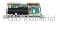
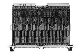
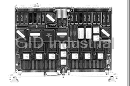


What they say about us
FANTASTIC RESOURCE
One of our top priorities is maintaining our business with precision, and we are constantly looking for affiliates that can help us achieve our goal. With the aid of GID Industrial, our obsolete product management has never been more efficient. They have been a great resource to our company, and have quickly become a go-to supplier on our list!
Bucher Emhart Glass
EXCELLENT SERVICE
With our strict fundamentals and high expectations, we were surprised when we came across GID Industrial and their competitive pricing. When we approached them with our issue, they were incredibly confident in being able to provide us with a seamless solution at the best price for us. GID Industrial quickly understood our needs and provided us with excellent service, as well as fully tested product to ensure what we received would be the right fit for our company.
Fuji
HARD TO FIND A BETTER PROVIDER
Our company provides services to aid in the manufacture of technological products, such as semiconductors and flat panel displays, and often searching for distributors of obsolete product we require can waste time and money. Finding GID Industrial proved to be a great asset to our company, with cost effective solutions and superior knowledge on all of their materials, it’d be hard to find a better provider of obsolete or hard to find products.
Applied Materials
CONSISTENTLY DELIVERS QUALITY SOLUTIONS
Over the years, the equipment used in our company becomes discontinued, but they’re still of great use to us and our customers. Once these products are no longer available through the manufacturer, finding a reliable, quick supplier is a necessity, and luckily for us, GID Industrial has provided the most trustworthy, quality solutions to our obsolete component needs.
Nidec Vamco
TERRIFIC RESOURCE
This company has been a terrific help to us (I work for Trican Well Service) in sourcing the Micron Ram Memory we needed for our Siemens computers. Great service! And great pricing! I know when the product is shipping and when it will arrive, all the way through the ordering process.
Trican Well Service
GO TO SOURCE
When I can't find an obsolete part, I first call GID and they'll come up with my parts every time. Great customer service and follow up as well. Scott emails me from time to time to touch base and see if we're having trouble finding something.....which is often with our 25 yr old equipment.
ConAgra Foods