PENT/CPCI-731
Installation Guide
P/N 213021 Revision AD
August 2001
Copyright
The information in this publication is subject to change without notice. Force Computers, GmbH reserves the right to make
changes without notice to this, or any of its products, to improve reliability, performance, or design.
Force Computers, GmbH shall not be liable for technical or editorial errors or omissions contained herein, nor for indirect, special,
incidental, or consequential damages resulting from the furnishing, performance, or use of this material. This information is pro-
vided “as is” and Force Computers, GmbH expressly disclaims any and all warranties, express, implied, statutory, or otherwise,
including without limitation, any express, statutory, or implied warranty of merchantability, fitness for a particular purpose, or
non-infringement.
This publication contains information protected by copyright. This publication shall not be reproduced, transmitted, or stored in
a retrieval system, nor its contents used for any purpose, without the prior written consent of Force Computers, GmbH.
Force Computers, GmbH assumes no responsibility for the use of any circuitry other than circuitry that is part of a product of
Force Computers, GmbH. Force Computers, GmbH does not convey to the purchaser of the product described herein any license
under the patent rights of Force Computers, GmbH nor the rights of others.
Copyright 2001 by Force Computers, GmbH. All rights reserved.
The Force logo is a trademark of Force Computers, GmbH.
IEEE is a registered trademark of the Institute for Electrical and Electronics Engineers, Inc.
PICMG, CompactPCI, and the CompactPCI logo are registered trademarks and the PICMG logo is a trademark of the PCI Indus-
trial Computer Manufacturer’s Group.
MS-DOS, Windows95, Windows98, Windows2000 and Windows NT are registered trademarks and the logos are a trademark of
the Microsoft Corporation.
Intel and Pentium are registered trademarks and the Intel logo is a trademark of the Intel Corporation.
Other product names mentioned herein may be trademarks and/or registered trademarks of their respective companies.
World Wide Web: www.forcecomputers.com
24-hour access to on-line manuals, driver updates, and application
notes is provided via SMART, our SolutionsPLUS customer support
program that provides current technical and services information.
Headquarters
The Americas Europe Asia
Force Computers Inc. Force Computers GmbH Force Computers Japan KK
5799 Fontanoso Way Prof.-Messerschmitt-Str. 1 Shiba Daimon MF Building 4F
San Jose, CA 95138-1015 D-85579 Neubiberg/München 2-1-16 Shiba Daimon
U.S.A. Germany Minato-ku, Tokyo 105-0012 Japan
Tel.: +1 (408) 369-6000 Tel.: +49 (89) 608 14-0 Tel.: +81 (03) 3437 3948
Fax: +1 (408) 371-3382 Fax: +49 (89) 609 77 93 Fax: +81 (03) 3437 3968
Email: support@fci.com Email: support@force.de Email: smiyagawa@fci.com
213021 420 000 AD
Contents
Using This Manual
Other Sources of Information
Safety Notes
Sicherheitshinweise
1 Introduction
Features . . . . . . . . . . . . . . . . . . . . . . . . . . . . . . . . . . . . . . . . . . . . . . . . . . . . . . . . . 1-3
CPU . . . . . . . . . . . . . . . . . . . . . . . . . . . . . . . . . . . . . . . . . . . . . . . . . . . . . . . . . . . . . . . . . . . . . . . . . . 1-4
Memory . . . . . . . . . . . . . . . . . . . . . . . . . . . . . . . . . . . . . . . . . . . . . . . . . . . . . . . . . . . . . . . . . . . . . . . . 1-4
Interfaces . . . . . . . . . . . . . . . . . . . . . . . . . . . . . . . . . . . . . . . . . . . . . . . . . . . . . . . . . . . . . . . . . . . . . . 1-5
Block Diagram . . . . . . . . . . . . . . . . . . . . . . . . . . . . . . . . . . . . . . . . . . . . . . . . . . . 1-6
Standard Compliance . . . . . . . . . . . . . . . . . . . . . . . . . . . . . . . . . . . . . . . . . . . . . . 1-7
Ordering Information . . . . . . . . . . . . . . . . . . . . . . . . . . . . . . . . . . . . . . . . . . . . . . 1-8
Product Nomenclature . . . . . . . . . . . . . . . . . . . . . . . . . . . . . . . . . . . . . . . . . . . . . . . . . . . . . . . . . . . . 1-8
Order Numbers . . . . . . . . . . . . . . . . . . . . . . . . . . . . . . . . . . . . . . . . . . . . . . . . . . . . . . . . . . . . . . . . . . 1-9
PENT/CPCI-731 v
2Installation
Action Plan . . . . . . . . . . . . . . . . . . . . . . . . . . . . . . . . . . . . . . . . . . . . . . . . . . . . . . 2-3
Requirements . . . . . . . . . . . . . . . . . . . . . . . . . . . . . . . . . . . . . . . . . . . . . . . . . . . . 2-4
Environmental Requirements . . . . . . . . . . . . . . . . . . . . . . . . . . . . . . . . . . . . . . . . . . . . . . . . . . . . . . . 2-4
Power Requirements . . . . . . . . . . . . . . . . . . . . . . . . . . . . . . . . . . . . . . . . . . . . . . . . . . . . . . . . . . . . . 2-6
Hardware Upgrades and Accessories . . . . . . . . . . . . . . . . . . . . . . . . . . . . . . . . 2-7
Memory Module . . . . . . . . . . . . . . . . . . . . . . . . . . . . . . . . . . . . . . . . . . . . . . . . . . . . . . . . . . . . . . . . . 2-7
PMC Module . . . . . . . . . . . . . . . . . . . . . . . . . . . . . . . . . . . . . . . . . . . . . . . . . . . . . . . . . . . . . . . . . . . 2-7
Slots 1 and 2 . . . . . . . . . . . . . . . . . . . . . . . . . . . . . . . . . . . . . . . . . . . . . . . . . . . . . . . . . . . . . . . . . 2-8
Voltage Keys . . . . . . . . . . . . . . . . . . . . . . . . . . . . . . . . . . . . . . . . . . . . . . . . . . . . . . . . . . . . . . . . . 2-8
Connector Configuration . . . . . . . . . . . . . . . . . . . . . . . . . . . . . . . . . . . . . . . . . . . . . . . . . . . . . . . . 2-8
Installing the PMC Module . . . . . . . . . . . . . . . . . . . . . . . . . . . . . . . . . . . . . . . . . . . . . . . . . . . . . . 2-9
Removing the PMC Module . . . . . . . . . . . . . . . . . . . . . . . . . . . . . . . . . . . . . . . . . . . . . . . . . . . . 2-11
VGA-Acc-Kit . . . . . . . . . . . . . . . . . . . . . . . . . . . . . . . . . . . . . . . . . . . . . . . . . . . . . . . . . . . . . . . . . . . 2-11
IDE Devices . . . . . . . . . . . . . . . . . . . . . . . . . . . . . . . . . . . . . . . . . . . . . . . . . . . . . . . . . . . . . . . . . . . 2-12
HD-Accessory Kit . . . . . . . . . . . . . . . . . . . . . . . . . . . . . . . . . . . . . . . . . . . . . . . . . . . . . . . . . . . . 2-13
IOBP-CPCI-731 . . . . . . . . . . . . . . . . . . . . . . . . . . . . . . . . . . . . . . . . . . . . . . . . . . . . . . . . . . . . . . . . 2-13
Floppy Disk Connection . . . . . . . . . . . . . . . . . . . . . . . . . . . . . . . . . . . . . . . . . . . . . . . . . . . . . . . . . . 2-14
Switch Settings . . . . . . . . . . . . . . . . . . . . . . . . . . . . . . . . . . . . . . . . . . . . . . . . . . 2-15
Board Installation . . . . . . . . . . . . . . . . . . . . . . . . . . . . . . . . . . . . . . . . . . . . . . . . 2-17
Signaling Level . . . . . . . . . . . . . . . . . . . . . . . . . . . . . . . . . . . . . . . . . . . . . . . . . . . . . . . . . . . . . . . . . 2-17
Installation in a Non-Powered System . . . . . . . . . . . . . . . . . . . . . . . . . . . . . . . . . . . . . . . . . . . . . . . 2-17
Installing the PENT/CPCI-731 . . . . . . . . . . . . . . . . . . . . . . . . . . . . . . . . . . . . . . . . . . . . . . . . . . 2-17
Removing the PENT/CPCI-731 . . . . . . . . . . . . . . . . . . . . . . . . . . . . . . . . . . . . . . . . . . . . . . . . . 2-18
Installation in a Powered System Supporting Hot Swap . . . . . . . . . . . . . . . . . . . . . . . . . . . . . . . . . 2-19
Installing the PENT/CPCI-731 . . . . . . . . . . . . . . . . . . . . . . . . . . . . . . . . . . . . . . . . . . . . . . . . . . 2-19
Removing the PENT/CPCI-731 . . . . . . . . . . . . . . . . . . . . . . . . . . . . . . . . . . . . . . . . . . . . . . . . . 2-20
Software Upgrades and Accessories . . . . . . . . . . . . . . . . . . . . . . . . . . . . . . . . 2-21
Maintenance . . . . . . . . . . . . . . . . . . . . . . . . . . . . . . . . . . . . . . . . . . . . . . . . . . . . 2-22
Battery . . . . . . . . . . . . . . . . . . . . . . . . . . . . . . . . . . . . . . . . . . . . . . . . . . . . . . . . . . . . . . . . . . . . . . . 2-22
vi PENT/CPCI-731
3 Controls, Indicators, and Connectors
Front Panel . . . . . . . . . . . . . . . . . . . . . . . . . . . . . . . . . . . . . . . . . . . . . . . . . . . . . . 3-3
PMC Cutouts . . . . . . . . . . . . . . . . . . . . . . . . . . . . . . . . . . . . . . . . . . . . . . . . . . . . . . . . . . . . . . . . . . . 3-4
LEDs . . . . . . . . . . . . . . . . . . . . . . . . . . . . . . . . . . . . . . . . . . . . . . . . . . . . . . . . . . . . . . . . . . . . . . . . . . 3-5
Keys . . . . . . . . . . . . . . . . . . . . . . . . . . . . . . . . . . . . . . . . . . . . . . . . . . . . . . . . . . . . . . . . . . . . . . . . . . 3-6
Connectors . . . . . . . . . . . . . . . . . . . . . . . . . . . . . . . . . . . . . . . . . . . . . . . . . . . . . . . . . . . . . . . . . . . . . 3-7
CompactPCI Connectors . . . . . . . . . . . . . . . . . . . . . . . . . . . . . . . . . . . . . . . . . . . 3-8
J1 and J2 . . . . . . . . . . . . . . . . . . . . . . . . . . . . . . . . . . . . . . . . . . . . . . . . . . . . . . . . . . . . . . . . . . . . . . 3-8
J3 . . . . . . . . . . . . . . . . . . . . . . . . . . . . . . . . . . . . . . . . . . . . . . . . . . . . . . . . . . . . . . . . . . . . . . . . . . . . 3-8
J4 . . . . . . . . . . . . . . . . . . . . . . . . . . . . . . . . . . . . . . . . . . . . . . . . . . . . . . . . . . . . . . . . . . . . . . . . . . . 3-10
J5 . . . . . . . . . . . . . . . . . . . . . . . . . . . . . . . . . . . . . . . . . . . . . . . . . . . . . . . . . . . . . . . . . . . . . . . . . . . 3-11
4BIOS
Introduction . . . . . . . . . . . . . . . . . . . . . . . . . . . . . . . . . . . . . . . . . . . . . . . . . . . . . . 4-3
Changing Configuration Settings . . . . . . . . . . . . . . . . . . . . . . . . . . . . . . . . . . . . 4-4
Selecting the Boot Device . . . . . . . . . . . . . . . . . . . . . . . . . . . . . . . . . . . . . . . . . . 4-5
Via Setup . . . . . . . . . . . . . . . . . . . . . . . . . . . . . . . . . . . . . . . . . . . . . . . . . . . . . . . . . . . . . . . . . . . . . . 4-5
Via Boot Selection Menu . . . . . . . . . . . . . . . . . . . . . . . . . . . . . . . . . . . . . . . . . . . . . . . . . . . . . . . . . . 4-6
Serial Console Redirection . . . . . . . . . . . . . . . . . . . . . . . . . . . . . . . . . . . . . . . . . 4-7
Requirements . . . . . . . . . . . . . . . . . . . . . . . . . . . . . . . . . . . . . . . . . . . . . . . . . . . . . . . . . . . . . . . . . . . 4-7
Remote Configuration . . . . . . . . . . . . . . . . . . . . . . . . . . . . . . . . . . . . . . . . . . . . . . . . . . . . . . . . . . . . . 4-8
Remote Configuration Set . . . . . . . . . . . . . . . . . . . . . . . . . . . . . . . . . . . . . . . . . . . . . . . . . . . . . . . 4-8
Remote Configuration Not Set . . . . . . . . . . . . . . . . . . . . . . . . . . . . . . . . . . . . . . . . . . . . . . . . . . . . 4-8
Updating BIOS via Software . . . . . . . . . . . . . . . . . . . . . . . . . . . . . . . . . . . . . . . . 4-9
BIOS Messages . . . . . . . . . . . . . . . . . . . . . . . . . . . . . . . . . . . . . . . . . . . . . . . . . . . 4-9
PENT/CPCI-731 vii
5 Buses
2
Board Information I C Bus . . . . . . . . . . . . . . . . . . . . . . . . . . . . . . . . . . . . . . . . . . 5-3
System Management Bus . . . . . . . . . . . . . . . . . . . . . . . . . . . . . . . . . . . . . . . . . . 5-4
6 Maps and Registers
Overview . . . . . . . . . . . . . . . . . . . . . . . . . . . . . . . . . . . . . . . . . . . . . . . . . . . . . . . . 6-3
I/O and Memory Maps . . . . . . . . . . . . . . . . . . . . . . . . . . . . . . . . . . . . . . . . . . . . . . 6-4
PENT/CPCI-731 Registers . . . . . . . . . . . . . . . . . . . . . . . . . . . . . . . . . . . . . . . . . . 6-6
ISA-Bus Decoding . . . . . . . . . . . . . . . . . . . . . . . . . . . . . . . . . . . . . . . . . . . . . . . . . . . . . . . . . . . . . . . 6-7
Flash Control Register . . . . . . . . . . . . . . . . . . . . . . . . . . . . . . . . . . . . . . . . . . . . . . . . . . . . . . . . . 6-8
2
I C Register . . . . . . . . . . . . . . . . . . . . . . . . . . . . . . . . . . . . . . . . . . . . . . . . . . . . . . . . . . . . . . . . . 6-9
Reset . . . . . . . . . . . . . . . . . . . . . . . . . . . . . . . . . . . . . . . . . . . . . . . . . . . . . . . . . . . . . . . . . . . . . . . . . 6-9
NMI/Reset Sources . . . . . . . . . . . . . . . . . . . . . . . . . . . . . . . . . . . . . . . . . . . . . . . . . . . . . . . . . . . 6-10
Reset Control Register . . . . . . . . . . . . . . . . . . . . . . . . . . . . . . . . . . . . . . . . . . . . . . . . . . . . . . . . 6-11
NMI Control Register . . . . . . . . . . . . . . . . . . . . . . . . . . . . . . . . . . . . . . . . . . . . . . . . . . . . . . . . . 6-14
Reset/NMI Status Register . . . . . . . . . . . . . . . . . . . . . . . . . . . . . . . . . . . . . . . . . . . . . . . . . . . . . 6-15
Software NMI/Reset Register . . . . . . . . . . . . . . . . . . . . . . . . . . . . . . . . . . . . . . . . . . . . . . . . . . . 6-16
Watchdog Retrigger and Watchdog Timer . . . . . . . . . . . . . . . . . . . . . . . . . . . . . . . . . . . . . . . . . . . . 6-17
PCI Configuration and Interrupt, Operating Modus . . . . . . . . . . . . . . . . . . . . . . . . . . . . . . . . . . . . . 6-19
Interrupt and ENUM Service Mode . . . . . . . . . . . . . . . . . . . . . . . . . . . . . . . . . . . . . . . . . . . . . . . 6-19
Signal Direction . . . . . . . . . . . . . . . . . . . . . . . . . . . . . . . . . . . . . . . . . . . . . . . . . . . . . . . . . . . . . . 6-19
Interrupt Mask . . . . . . . . . . . . . . . . . . . . . . . . . . . . . . . . . . . . . . . . . . . . . . . . . . . . . . . . . . . . . . . 6-20
PCI Control Register . . . . . . . . . . . . . . . . . . . . . . . . . . . . . . . . . . . . . . . . . . . . . . . . . . . . . . . . . . 6-20
PCI Interrupt Control Register . . . . . . . . . . . . . . . . . . . . . . . . . . . . . . . . . . . . . . . . . . . . . . . . . . 6-21
Geographical Addressing and Rear Transition Module . . . . . . . . . . . . . . . . . . . . . . . . . . . . . . . . . . 6-22
Geographical Address . . . . . . . . . . . . . . . . . . . . . . . . . . . . . . . . . . . . . . . . . . . . . . . . . . . . . . . . 6-22
Rear Transition Module Detection . . . . . . . . . . . . . . . . . . . . . . . . . . . . . . . . . . . . . . . . . . . . . . . 6-23
Hot-Swap ENUM Register . . . . . . . . . . . . . . . . . . . . . . . . . . . . . . . . . . . . . . . . . . . . . . . . . . . . . . . . 6-23
LED Control Register . . . . . . . . . . . . . . . . . . . . . . . . . . . . . . . . . . . . . . . . . . . . . . . . . . . . . . . . . . . . 6-24
Register Lock and Page Function . . . . . . . . . . . . . . . . . . . . . . . . . . . . . . . . . . . . . . . . . . . . . . . . . . 6-25
Flag Register . . . . . . . . . . . . . . . . . . . . . . . . . . . . . . . . . . . . . . . . . . . . . . . . . . . . . . . . . . . . . . . . . . 6-25
Version Register . . . . . . . . . . . . . . . . . . . . . . . . . . . . . . . . . . . . . . . . . . . . . . . . . . . . . . . . . . . . . . . 6-26
Spare Configuration Switches . . . . . . . . . . . . . . . . . . . . . . . . . . . . . . . . . . . . . . 6-27
viii PENT/CPCI-731
PMC Slot Identification . . . . . . . . . . . . . . . . . . . . . . . . . . . . . . . . . . . . . . . . . . . . 6-28
Hardware Monitor . . . . . . . . . . . . . . . . . . . . . . . . . . . . . . . . . . . . . . . . . . . . . . . . 6-29
Troubleshooting . . . . . . . . . . . . . . . . . . . . . . . . . . . . . . . . . . . . . . . . . . . . . . . . . . A-3
Index
Product Error Report
PENT/CPCI-731 ix
x PENT/CPCI-731
Tables
Introduction
Table 1 Interfaces . . . . . . . . . . . . . . . . . . . . . . . . . . . . . . . . . . . . . . . . . . . . . . . . . . . . . . . . . . 1-5
Table 2 Standard Compliance. . . . . . . . . . . . . . . . . . . . . . . . . . . . . . . . . . . . . . . . . . . . . . . . . 1-7
Table 3 Nomenclature. . . . . . . . . . . . . . . . . . . . . . . . . . . . . . . . . . . . . . . . . . . . . . . . . . . . . . . 1-8
Table 4 Ordering Information Excerpt . . . . . . . . . . . . . . . . . . . . . . . . . . . . . . . . . . . . . . . . . . 1-9
Installation
Table 5 Environmental Requirements. . . . . . . . . . . . . . . . . . . . . . . . . . . . . . . . . . . . . . . . . . . 2-5
Table 6 PENT/CPCI-731 Switch Settings . . . . . . . . . . . . . . . . . . . . . . . . . . . . . . . . . . . . . . . 2-15
Controls, Indicators, and Connectors
Table 7 Description of Front Panel LEDs . . . . . . . . . . . . . . . . . . . . . . . . . . . . . . . . . . . . . . . . 3-5
Buses
2
Table 8 Devices on Module Information I C Bus . . . . . . . . . . . . . . . . . . . . . . . . . . . . . . . . . . 5-3
2
Table 9 Devices on System Management I C Bus . . . . . . . . . . . . . . . . . . . . . . . . . . . . . . . . . 5-4
Maps and Registers
Table 10 Register Overview . . . . . . . . . . . . . . . . . . . . . . . . . . . . . . . . . . . . . . . . . . . . . . . . . . . 6-3
Table 11 I/O Map . . . . . . . . . . . . . . . . . . . . . . . . . . . . . . . . . . . . . . . . . . . . . . . . . . . . . . . . . . . 6-4
Table 12 Register on Page 1 Overview . . . . . . . . . . . . . . . . . . . . . . . . . . . . . . . . . . . . . . . . . . 6-6
Table 13 Register on Page 2 Overview . . . . . . . . . . . . . . . . . . . . . . . . . . . . . . . . . . . . . . . . . . 6-6
Table 14 Flash Control Register . . . . . . . . . . . . . . . . . . . . . . . . . . . . . . . . . . . . . . . . . . . . . . . . 6-8
2
Table 15 I C Register . . . . . . . . . . . . . . . . . . . . . . . . . . . . . . . . . . . . . . . . . . . . . . . . . . . . . . . . 6-9
Table 16 NMI/Reset Sources . . . . . . . . . . . . . . . . . . . . . . . . . . . . . . . . . . . . . . . . . . . . . . . . . 6-10
Table 17 Possible NMI/Reset Configurations . . . . . . . . . . . . . . . . . . . . . . . . . . . . . . . . . . . . . 6-11
Table 18 Reset Control Register 1 . . . . . . . . . . . . . . . . . . . . . . . . . . . . . . . . . . . . . . . . . . . . . 6-11
PENT/CPCI-731 xi
Table 19 Reset Control Register 2 . . . . . . . . . . . . . . . . . . . . . . . . . . . . . . . . . . . . . . . . . . . . . 6-12
Table 20 NMI Control Register. . . . . . . . . . . . . . . . . . . . . . . . . . . . . . . . . . . . . . . . . . . . . . . . 6-14
Table 21 Reset/NMI Status Register . . . . . . . . . . . . . . . . . . . . . . . . . . . . . . . . . . . . . . . . . . . 6-15
Table 22 Software NMI/Reset Register . . . . . . . . . . . . . . . . . . . . . . . . . . . . . . . . . . . . . . . . . 6-16
Table 23 Watchdog Timer . . . . . . . . . . . . . . . . . . . . . . . . . . . . . . . . . . . . . . . . . . . . . . . . . . . 6-17
Table 24 Watchdog Timer Register . . . . . . . . . . . . . . . . . . . . . . . . . . . . . . . . . . . . . . . . . . . . 6-18
Table 25 Signal Direction . . . . . . . . . . . . . . . . . . . . . . . . . . . . . . . . . . . . . . . . . . . . . . . . . . . . 6-19
Table 26 PCI Control Register . . . . . . . . . . . . . . . . . . . . . . . . . . . . . . . . . . . . . . . . . . . . . . . . 6-20
Table 27 PCI Interrupt Control Register . . . . . . . . . . . . . . . . . . . . . . . . . . . . . . . . . . . . . . . . . 6-21
Table 28 Geographical Address Register . . . . . . . . . . . . . . . . . . . . . . . . . . . . . . . . . . . . . . . 6-22
Table 29 TM_PRNT Signal . . . . . . . . . . . . . . . . . . . . . . . . . . . . . . . . . . . . . . . . . . . . . . . . . . 6-23
Table 30 Hot-Swap ENUM Register. . . . . . . . . . . . . . . . . . . . . . . . . . . . . . . . . . . . . . . . . . . . 6-23
Table 31 LED Control Register . . . . . . . . . . . . . . . . . . . . . . . . . . . . . . . . . . . . . . . . . . . . . . . 6-24
Table 32 Lock and Page Register . . . . . . . . . . . . . . . . . . . . . . . . . . . . . . . . . . . . . . . . . . . . . 6-25
Table 33 Flag Register. . . . . . . . . . . . . . . . . . . . . . . . . . . . . . . . . . . . . . . . . . . . . . . . . . . . . . 6-25
Table 34 Version Register . . . . . . . . . . . . . . . . . . . . . . . . . . . . . . . . . . . . . . . . . . . . . . . . . . . 6-26
Table 35 Configuration Switches . . . . . . . . . . . . . . . . . . . . . . . . . . . . . . . . . . . . . . . . . . . . . . 6-27
Table 36 Busmode/GPIO Routing . . . . . . . . . . . . . . . . . . . . . . . . . . . . . . . . . . . . . . . . . . . . . 6-28
Table 37 General Purpose I/O Registers in Intel21150 . . . . . . . . . . . . . . . . . . . . . . . . . . . . . 6-28
Table 38 Monitored Board Voltages versus Hardware Monitor Voltage Inputs . . . . . . . . . . . 6-29
Table 39 Hardware Monitor Base Address . . . . . . . . . . . . . . . . . . . . . . . . . . . . . . . . . . . . . . 6-30
xii PENT/CPCI-731
Figures
Introduction
Figure 1 Function Blocks . . . . . . . . . . . . . . . . . . . . . . . . . . . . . . . . . . . . . . . . . . . . . . . . . . . . .1-3
Figure 2 Block Diagram . . . . . . . . . . . . . . . . . . . . . . . . . . . . . . . . . . . . . . . . . . . . . . . . . . . . . .1-6
Installation
Figure 3 Voltage Keys . . . . . . . . . . . . . . . . . . . . . . . . . . . . . . . . . . . . . . . . . . . . . . . . . . . . . . .2-8
Figure 4 PMC Connectors and Slots . . . . . . . . . . . . . . . . . . . . . . . . . . . . . . . . . . . . . . . . . . . 2-10
Figure 5 Position of Mounting Holes . . . . . . . . . . . . . . . . . . . . . . . . . . . . . . . . . . . . . . . . . . . 2-11
Figure 6 Flash Disk and IDE Connector . . . . . . . . . . . . . . . . . . . . . . . . . . . . . . . . . . . . . . . . 2-12
Figure 7 Floppy Connector . . . . . . . . . . . . . . . . . . . . . . . . . . . . . . . . . . . . . . . . . . . . . . . . . . 2-14
Figure 8 Switch Sets . . . . . . . . . . . . . . . . . . . . . . . . . . . . . . . . . . . . . . . . . . . . . . . . . . . . . . .2-15
Controls, Indicators, and Connectors
Figure 9 PENT/CPCI-731 Front Panel . . . . . . . . . . . . . . . . . . . . . . . . . . . . . . . . . . . . . . . . . . 3-3
Figure 10 Cutouts for PMC Modules . . . . . . . . . . . . . . . . . . . . . . . . . . . . . . . . . . . . . . . . . . . . . 3-4
Figure 11 KBD/MS - Keyboard and Mouse Connector Pinout . . . . . . . . . . . . . . . . . . . . . . . . . 3-7
Figure 12 COM1 Connector Pinout . . . . . . . . . . . . . . . . . . . . . . . . . . . . . . . . . . . . . . . . . . . . . . 3-7
Figure 13 CompactPCI J3 Connector Pinout . . . . . . . . . . . . . . . . . . . . . . . . . . . . . . . . . . . . . . 3-9
Figure 14 CompactPCI J4 Connector Pinout . . . . . . . . . . . . . . . . . . . . . . . . . . . . . . . . . . . . . 3-10
Figure 15 CompactPCI J5 Connector Pinout . . . . . . . . . . . . . . . . . . . . . . . . . . . . . . . . . . . . . 3-11
BIOS
Figure 16 Main Menu . . . . . . . . . . . . . . . . . . . . . . . . . . . . . . . . . . . . . . . . . . . . . . . . . . . . . . . . 4-4
Figure 17 Boot Device Order . . . . . . . . . . . . . . . . . . . . . . . . . . . . . . . . . . . . . . . . . . . . . . . . . . . 4-5
Figure 18 Boot Menu . . . . . . . . . . . . . . . . . . . . . . . . . . . . . . . . . . . . . . . . . . . . . . . . . . . . . . . . . 4-6
PENT/CPCI-731 xiii
Maps and Registers
Figure 19 Memory Map . . . . . . . . . . . . . . . . . . . . . . . . . . . . . . . . . . . . . . . . . . . . . . . . . . . . . . 6-5
Figure 20 Flash Device Address Mapping . . . . . . . . . . . . . . . . . . . . . . . . . . . . . . . . . . . . . . . . 6-7
xiv PENT/CPCI-731
Using This Manual
This Installation Guide is intended for users qualified in electronics or elec-
trical engineering. Users must have a working understanding of Peripheral
Component Interconnect (PCI), Compact Peripheral Component Intercon-
nect (CPCI), and telecommunications.
Conventions
Notation Description
1234 All numbers are decimal numbers except when used with the
notations described below.
00000000 Typical notation for hexadecimal numbers (digits are 0 through
16
F), e.g. used for addresses and offsets
0000 Same for binary numbers (digits are 0 and 1)
2
x Generic use of a letter
n Generic use of numbers
n.nn Decimal point indicator is signaled
Bold Character format used to emphasize a word
Italics
Character format for references, table, and figure descriptions
Typical notation used for variables and keys
[text] Typical notation for buttons
No danger encountered. Pay attention to important information
Note: marked using this layout.
Caution Possibly dangerous situation: slight injuries to people or damage
to objects possible
Danger Dangerous situation: injuries to people or severe damage to
objects possible
PENT/CPCI-731 xv
Revision History
Order No. Revision Date Description
211605 1.0 December 1999 First Print
211605 2.0 February 2000 Corrected Forced Air Flow in Table 5
“Environmental Requirements” on
page 2-5
213021 AA June 2000 Changed SW2-3 to ON in Table 6
“PENT/CPCI-731 Switch Settings” on
page 2-15;
Corrected the “BIOS” section on page 4-
1;
Merged Reference Guide with SAP
No. 211605 to Installation Guide with
SAP No. 213021;
editorial changes
213021 AB March 2001 Revised layout of Installation Guide;
Corrected default setting of second bit in
Table 18 “Reset Control Register 1” on
page 6-11;
Added the “Troubleshooting” section on
page 7-1
213021 AC July 2001 Corrected information on default setting
of white switches in the “Switch Set-
tings” section on page 2-15;
Updated the “BIOS” section on page 4-1;
Removed Troubleshooting section;
Added the “Appendix” section on
page A-1;
Added the “Index” section on page I-1;
Editorial changes;
213021 AD August 2001 Added the “Sicherheitshinweise” sec-
tion on page -xxiii
xvi PENT/CPCI-731
Other Sources of Information
For further information refer to the following documents:
Company Web Address Documents
Force Computers www.forcecomput- PENT/CPCI-730 Installation
ers.com Guide (P/N 212399)
PENT/CPCI-731/HD-AccKit
IOBP-CPCI-731
Intel www.devel- BIOS flash: 1Mx8, 28F008S5
oper.intel.com
CPU: Intel Pentium II
Intel Pentium II Processore
Mobile Module: Mobile module
connector 2 (MMC-2)
Intel Architecture Software
Developer’s Manual
Volume 1: Basic Architecture
Volume 2: Instruction Set Refer-
ence Manual
Volume 3: System Programming
Guide
EIDE, PCI-to-ISA bridge, USB:
82371AB (82371EB)
Ethernet: 82559
Host-to-PCI bridge: 82443BX
PCI-to-PCI bridge: 21150
PCI-to-PCI bridge: 21554
Hitachi/Micron/ www.halsp.hitachi.com 8Mx8 (M5M4V64S30A) SRAM
Mitsubishi
National www.national.com Keyboard, PS2 mouse, COM1,
COM2, LPT1, floppy: PC87309
SuperI/O
2
Philips Semiconduc- www. philips.com The I C bus and how to use it
tor (including specifications)
SanDisk www.sandisk.com IDE flash disk: Flash Chipset,
SDFCSTB-128-366
Winbond www.winbond.com Hardware monitor: W83781D
PENT/CPCI-731 xvii
xviii PENT/CPCI-731
Safety Notes
This section provides safety precautions to follow when installing, operat-
ing, and maintaining the PENT/CPCI-731. For your protection, follow all
warnings and instructions found in the following text.
This Installation Guide provides the necessary information to install and
handle the PENT/CPCI-731. As the product is complex and its usage mani-
fold, we do not guarantee that the given information is complete. If you
need additional information, ask your Force Computers representative.
The PENT/CPCI-731 has been designed to meet the standard industrial
safety requirements. It must not be used except in its specific area of
office telecommunication industry and industrial control.
Only personnel trained by Force Computers or persons qualified in elec-
tronics or electrical engineering are authorized to install, uninstall or
maintain the PENT/CPCI-731. The information given in this manual is
meant to complete the knowledge of a specialist and must not be taken as
replacement for qualified personnel.
EMC
The board has been tested in a Standard Force Computers system and
found to comply with the limits for a Class A digital device in this sys-
tem, pursuant to part 15 of the FCC Rules respectively EN 55022 Class A.
These limits are designed to provide reasonable protection against harm-
ful interference when the system is operated in a commercial environ-
ment.
The board generates, uses and can radiate radio frequency energy and, if
not installed properly and used in accordance with this Installation
Guide, may cause harmful interference to radio communications. Operat-
ing the system in a residential area is likely to cause harmful interfer-
ence, in which case the user will be required to correct the interference at
his own expense.
If boards are integrated into open systems, always cover empty slots.
To ensure proper EMC shielding, always operate the PENT/CPCI-731
with the blind panels or with PMC modules installed.
PENT/CPCI-731 xix
Installation
Electrostatic discharge and incorrect board installation and removing can
damage circuits or shorten their life. Therefore:
• Before installing or removing the board, check the “Requirements”
section on page 2-4.
• Before touching integrated circuits, make sure that you are working
in an ESD-safe environment.
• When plugging the board in or removing it, do not press on the front
panel but use the handles.
• Before installing or removing an additional device or module, read
the respective documentation.
• Make sure that the board is connected to the CompactPCI backplane
via all assembled connectors and that power is available on all power
pins.
Operation
While operating the board ensure that the environmental and power
requirements are met.
When operating the board in areas of strong electromagnetic radiation
ensure that the board is bolted on the CompactPCI rack and shielded by
enclosure.
Make sure that contacts and cables of the board cannot be touched while
the board is operating.
Hot Swap
Never install or remove the board in a system under hot-swap conditions
unless the basic hot-swap, full hot-swap or high-availability platform is
used and the system documentation explicitly includes appropriate
guidelines.
xx PENT/CPCI-731
Expansion
Check the total power consumption of all components installed (see the
technical specification of the respective components).
Ensure that any individual output current of any source stays within its
acceptable limits (see the technical specification of the respective source).
Only replace components or system parts with those recommended by
Force Computers. Otherwise, you are fully responsible for the impact on
EMI and the possibly changed functionality of the product.
IOBP
The IOBP-CPCI-731 is especially designed for the base board of the
PENT/CPCI-731. Do not connect any other I/O panels with the
PENT/CPCI-731.
RJ-45 Connector
An RJ-45 connector is used for both telephone and twisted pair Ethernet
(TPE) connectors. Mismatching the two connectors may destroy your
telephone as well as your PENT/CPCI-731. Therefore:
• TPE connectors near your working area have to be clearly marked as
network connectors.
• TPE bushing of the system has to be connected only to safety extra
low voltages (SELV) circuits.
• The length of the electric cable connected to a TPE bushing must not
exceed 100 meter.
Battery
If a Lithium battery on the board has to be exchanged, observe the fol-
lowing safety notes:
• Incorrect exchange of Lithium batteries can result in a hazardous
explosion.
• Exchange the battery before five years of actual battery use have
elapsed.
• Exchanging the battery always results in data loss of the devices
which use the battery as a power backup. Therefore, back up affected
data before exchanging the battery.
PENT/CPCI-731 xxi
• Always use the same type of Lithium battery as is already installed.
• If the battery is covered by a PMC module on slot 1 or by a memory
module, the module must be removed first.
• Use an appropriate tool to remove the battery from its holder to avoid
possible damage to the board or the battery holder.
• When installing the new battery, ensure that the ’+’ on top of the bat-
tery stays at the top and therefore is visible when viewing the board
from its component side. If necessary, reinstall the PMC or memory
module in its correct position.
Environment
Always dispose of used batteries and/or old boards according to your
country’s legislation.
xxii PENT/CPCI-731
Sicherheitshinweise
Dieser Abschnitt enthält Sicherheitshinweise, welche bei der Installation,
dem Betrieb und der Wartung des PENT/CPCI-731 zu beachten sind.
Beachten Sie zu Ihrem Schutz alle folgenden Warnhinweise und Anleitun-
gen.
Dieses Installationshandbuch enthält alle notwendigen Informationen zur
Installation und zum Betrieb des PENT/CPCI-731. Da es sich um ein
komplexes Produkt mit einer aufwendigen Bedienung handelt, kann keine
Garantie dafür übernommen werden, dass die enthaltenen Informationen
vollständig sind. Für weitere Informationen wenden Sie sich bitte an Ihren
Vertreter der Firma Force Computers.
Das PENT/CPCI-731 erfüllt die gültigen industriellen Sicherheitsan-
forderungen. Dieses Produkt darf ausschließlich für Anwendungen
innerhalb der Telekommunikationsindustrie und der industriellen
Steuerung verwendet werden.
Lediglich von Force Computers eingewiesene oder im Bereich Elektro-
technik oder Elektronik qualifizierte Personen sind zur Installation, zum
Betrieb und zur Wartung dieses Produktes befugt. Die in dieser Doku-
mentation enthaltenen Informationen sollen lediglich als Hilfestellung
für entsprechend qualifiziertes Fachpersonal dienen. Keinesfalls kann es
dieses ersetzen.
EMV
Das Board wurde in einem Force Computers Standardsystem getestet
und entspricht den Grenzen eines Klasse-A-Produktes gemäß Abschnitt
15 der FCC-Richtlinien, insbesondere EN 55022 Klasse A.
Diese Grenzen sind dafür vorgesehen, einen vernünftigen Schutz gegen
störende Einflüsse bei einem Betrieb in einer kommerziellen Umgebung
zu gewährleisten.
Das Board erzeugt elektromagnetische Strahlung. Wird das System un-
sachgemäß installiert oder in anderer Weise als in diesem Installations-
handbuch beschrieben betrieben, kann es in der Umgebung von
Rundfunksendern und in Wohngegenden zu Störungen kommen. In
diesem Fall ist der Benutzer verpflichtet, entstehende Störungen auf
seine Kosten beheben zu lassen und die Kosten von Messungen selbst zu
tragen.
PENT/CPCI-731 xxiii
Werden Boards in offene Systeme eingebaut, müssen freie Steckplätze
mit einer Blende abgeschirmt werden.
Um eine ausreichende Abschirmung zu gewährleisten, darf das Board
nur mit einer Blindblende oder mit einer installierten PCMCIA-Karte
betrieben werden.
Installation
Elektrostatische Entladung und unsachgemäße Installation und Ausbau
des Boards kann Schaltkreise beschädigen oder ihre Lebensdauer
verkürzen. Deswegen sind folgende Punkte vor der Installation zu über-
prüfen:
• Lesen Sie vor Einbau oder Ausbau des Boards den Abschnitt
“Requirements” auf Seite 2-4
• Bevor Sie integrierte Schaltkreise berühren, vergewissern Sie sich,
dass Sie in einem ESD-geschützten Bereich arbeiten.
• Drücken Sie beim Einbau oder Ausbau des Boards nicht auf das Front
Panel, sondern benutzen Sie die Griffe.
• Lesen Sie vor dem Einbau oder Ausbau von zusätzlichen Geräten
oder Modulen das jeweilige Benutzerhandbuch.
• Vergewissern Sie sich, dass das Board über alle Stecker an die Com-
pactPCI Backplane angeschlossen ist und Strom an allen Power Pins
anliegt.
Betrieb
Während des Betriebs müssen die Umgebungs- und die Stromsversor-
gungsbedingungen gewährleistet sein.
Wenn das Board in Gebieten mit starker elektromagnetischer Strahlung
betrieben wird, stellen Sie sicher, dass das Board auf dem Compact PCI
Rack verschraubt ist und mit einem Gehäuse geschützt ist.
Es ist sicherzustellen, dass Anschlüsse und Kabel des Boards während
des Betriebs nicht versehentlich berührt werden können.
xxiv PENT/CPCI-731
Hot Swap
Einbau oder Ausbau des Boards in einem System unter Hot Swap Bedin-
gungen darf nur dann stattfinden, wenn die grundlegende Hot Swap
Plattform, die vollständige Hot Swap Plattform, oder die Hochverfüg-
barkeits Hot Swap Plattform benutzt wird und die Systembeschreibung
ausdrücklich die geeigneten Richtlinien vorgibt.
Erweiterung
Beachten Sie den Gesamtstromverbrauch aller installierter Kompo-
nenten (siehe technische Daten der entsprechenden Komponente).
Vergewissern Sie sich, daß jeder individuelle Ausgangsstrom jedes
Stromverbrauchers innerhalb der zulässigen Grenzwerte liegt (siehe
technische Daten des entsprechenden Verbrauchers).
Benutzen Sie bei der Erweiterung ausschließlich von Force Computers
empfohlene Komponenten und Systemteile. Ansonsten sind Sie für die
Auswirkungen auf EMV und die möglicherweise geänderte Funktional-
ität des Produktes verantwortlich.
IOBP
Das IOBP-CPCI-731 ist speziell für das Basis-Board der CPCI-731
entwickelt worden. Verwenden Sie kein anderes IOBP zusammen mit
der CPCI-731.
RJ-45 Stecker
RJ-45 Stecker werden sowohl für Telefonanschlüsse als auch für
Twisted-pair-Ethernet (TPE) verwendet. Die Verwechslung solcher
Anschlüsse kann sowohl das Telefonsystem als auch das Board zer-
stören. Daher:
• TPE-Anschlüsse in der Nähe Ihres Arbeitsplatzes müssen deutlich als
Netzwerkanschlüsse gekennzeichnet sein.
• An TPE-Buchsen dürfen nur SELV-Kreise angeschlossen werden
(Sicherheitskleinspannungsstromkreise).
• Die Länge der an einer TPE-Buchse angeschlossenen Leitung darf
nicht mehr als 100 Meter betragen.
PENT/CPCI-731 xxv
Batterie
Muss eine Lithium Batterie auf dem Board ausgetauscht werden, müssen
die folgenden Sicherheitshinweise beachtet werden:
• Fehlerhafter Austausch von Lithium Batterien kann zu lebensgefähr-
lichen Explosionen führen.
• Tauschen Sie die Batterie aus, bevor die fünf Jahre tatsächlicher
Betriebsdauer vorbei sind.
• Beim Austausch der Batterie gibt es immer einen Datenverlust bei
den Bausteinen, die die Batterie aus Notstromversorgung verwenden.
Sichern Sie deshalb die betroffenen Daten vor dem Austausch der
Batterie.
• Es darf nur der Batterietyp verwendet werden, der auch bereits ein-
gesetzt ist.
• Falls die Batterie von einem PMC Modul auf Steckplatz 1 oder von
einem Speichermodul verdeckt wird, muss erst das Modul entfernt
werden.
• Verwenden Sie zum Entfernen der Batterie aus dem Halter geeignetes
Werkzeug, um Schaden an Board oder Batteriehalter zu vermeiden.
• Vergewissern Sie sich beim Einbau einer neuen Batterie, dass das ’+’
oben auf der Batterie oben und damit sichtbar bleibt, wenn das Board
von der Komponentenseite betrachtet wird. Falls nötig, installieren
Sie das PMC-Modul oder das Speichermodul in der dafür vorgese-
henen Position.
Umweltschutz
Alte Batterien und/oder Boards oder Systeme müssen stets gemäß der in
Ihrem Land gültigen Gesetzgebung entsorgt werden.
xxvi PENT/CPCI-731
1
Introduction
Introduction Features
Features
The PENT/CPCI-731 is a 6U CompactPCI computer based on the Intel Pen-
tium III CPU and is a CompactPCI non-host or I/O board. It requires the
space of one slot. All PENT/CPCI-731 PCI buses are 32-bit wide and oper-
ate at 33 MHz PCI bus frequency.
The PENT/CPCI-731 is qualified to run with Windows NT Version 4.0. or
higher, VxWorks and LynxOS. It is provided with inrush current protection
and supports full hot swap.
One Serial
Keyboard
PMC2
PMC1
Port
Controller
2.5” EIDE
EIDE
Hard Disk
440BX Northbridge Flash disk
Pentium II
PCI-to-ISA PCI-to-PCI PCI-to-PCI
Bridge Bridge Bridge
L2 Cache
BANK 0
Watchdog
Super I/O
BANK 1
BANK 2-5
BIOS
ETH 0 ETH 1
1Mbyte flash
Figure 1: Function Blocks
PENT/CPCI-731 1 - 3
Features Introduction
CPU
The PENT/CPCI-731 offers a mobile module based on a Pentium II proces-
sor with 333 MHz speed or higher with 512 KByte L2 cache or a Pentium III
processor with 500 MHz speed with 256 KByte L2 cache.
Additional features are:
• Motorola 146818 compatible real-time clock and CMOS RAM for storing fac-
tory settings, both RTC and RAM with battery backup
• Program-readable vintage registers for board information protocol (BIP)
• Software-controllable, scalable watchdog, which controls the CPU activ-
ity and causes a RESET or an NMI in case of malfunction
• Two 82C37A compatible DMA controllers on the PCI-to-ISA bridge
• Two 82C29 compatible interrupt controllers on the PCI-to-ISA bridge
• 8254 compatible 3-channel timer
Memory
Memory features include:
• One MByte flash BIOS, 8-bit wide
• Optional 16 MByte flash disk
• Synchronous DRAM with ECC support running at 66 or 100 MHz clock
frequency
• Up to 768 MByte main memory with ECC, depending on selected mem-
ory option
1 - 4 PENT/CPCI-731
Introduction Features
Interfaces
The front panel and on-board interfaces of the PENT/CPCI-731 are shown
in the table below.
Table 1: Interfaces
Interface Description
Ethernet Two 10/100 BaseTEthernet available via CompactPCI con-
nector J5 (IOBP-CPCI-731)
Floppy Floppy controller via CompactPCI connector J4
IDE Primary IDE interface available via on-board connector
Secondary IDE interface available via CompactPCI connec-
tors J4 and J5
Keyboard/Mouse PS2 keyboard and mouse interface available on front panel
and on CompactPCI connector J5
Parallel I/O Parallel interface IEEE 1284, compatible with ECP (Exten-
dend Capabilities Port) and EPP (Extended Parallel Port) at
CompactPCI connector J4
PMC Two PMC interfaces, both supporting the front panel inter-
face and the rear interface via CompactPCI connectors J3 and
J5
Serial I/O Two serial interfaces
COM1 on front panel and on CompactPCI connector J3
COM2 on CompactPCI connector J3
USB Two USB interfaces available on CompactPCI connector J3
PENT/CPCI-731 1 - 5
Block Diagram Introduction
Block Diagram
This block diagram serves as an overview of how the PENT/CPCI-731
devices operate together and which data paths they use.
Ethernet LEDs
Ethernet 0
Ethernet 0
82559
EIDE(S)
Local PCI Bus 0, 3.3V J5
Ethernet 1
Ethernet 1
Ethernet LEDs
82559
Keybd., Mouse
Slot 0 Front Panel
PMC slot B
PMC Slot 2
Rear I/O
PMC Slot 1
EIDE(P)
Transparent Bridge
Slot 1 Front Panel
J4
Floppy, LPT
COM1 COM1/2
USB1/2
User Flash
Super I/O
16 MByte EIDE
PMC slot A
PC87309
Master
J3
EIDE
on-board
Up to 4 MByte
Watchdog/
Flash
Control
8 pages 512 KByte J2
440BX
Northbridge
Bank Bank Bank
0 1 2-5
Pentium II L2 Cache
64/ 64/ 512 MB
J1
128 MB 128 MB
Figure 2: Block Diagram
1 - 6 PENT/CPCI-731
Introduction Standard Compliance
Standard Compliance
The PENT/CPCI-731 complies with the following standards:
Table 2: Standard Compliance
Standard Description
IEC 68-2-1/2/3/13/14 Climatic environmental requirements.The
PENT/CPCI-731 can only be used in an
restricted temperature range (see Table 5
“Environmental Requirements” on page 2-5
for details.)
IEC 68-2-6/27/32 Mechanical environmental requirements
EN 609 50/UL 1950 (predefined Force Legal requirements
system);
UL 94V-0/1
EN 50081-1, EMC requirements on system level
EN 50082-2,
FCC Part 15 Class A
ANSI/IPC-A-610 Rev.B Class 2, Manufacturing requirements
ANSI/IPC-R-700B, ANSI-J-001...003
ISO 8601 Y2K compliance
PENT/CPCI-731 1 - 7
Ordering Information Introduction
Ordering Information
When ordering PENT/CPCI-731 board variants, upgrades, and accessories,
use the order numbers given below.
Product Nomenclature
The following table will provide you with the key for the product name
extensions.
Table 3: Nomenclature
PENT/CPCI-731//dd-ppp-Lccc-u
ddd DRAM size in MByte
ppp Processor clock frequency in MHz
Lccc L2 cache capacity in KByte
u MByte IDE flash disk
1 - 8 PENT/CPCI-731
Introduction Ordering Information
Order Numbers
The upgrades and accessories available depend on the variant of the
PENT/CPCI-731 under consideration. Consult your local sales representa-
tive to confirm availability of specific combinations.
1)
Table 4: Ordering Information Excerpt
Order No. PENT/CPCI-731 Description
106759 .../128-266-L512-0 Intel Pentium II 266 MHz with 128 MByte main
memory, 512 KByte L2 cache, no flash disk
106666 .../256-333-L256-16 Intel Pentium II 333 MHz with 256 MByte main
memory, 256 KByte L2 cache, 16 MByte flash
disk
107092 PENT/MEM-700/III III= 512 MByte memory module
107088 PMC/VGA-4 PMC based VGA graphics card and related
installation components
Accessories PENT/CPCI-731
106810 .../HD-AccKit Hard Disk and related installation components
106619 IOBP/CPCI-731 Rear transition board and related installation
components
Software Accessories PENT/CPCI-731
106710 .../BIOS Upgrade Kit BIOS upgrade utilities
1) Status: August 2001
PENT/CPCI-731 1 - 9
Ordering Information Introduction
1 - 10 PENT/CPCI-731
2
Installation
Installation Action Plan
Action Plan
In order to install the board, follow the procedure listed in the flow chart
below.
Start installation
Check “Requirements” on page 2-4
Hardware upgrades and NO
accessories to be installed?
YES
Page 2-7
Check “Switch Settings” on page 2-15
non-powered
system
Install the board
powered system
Page 2-17
Page 2-19
NO
IOBP to be
installed?
YES
Page 2-11
Software upgrades NO
and accessories to be
installed?
YES
Page 2-21
Installation finished
PENT/CPCI-731 2 - 3
Requirements Installation
Requirements
The PENT/CPCI-731 fulfills the standard Force Computers reliability
requirements for board products. It is a CompactPCI peripheral slot board.
The PCI bus supports 32-bit data bus width with a frequency of 33 MHz.
Caution Always install the PENT/CPCI-731 in a peripheral slot which is marked
by a circle. Otherwise, irreversible damage may occur to the board or to
the system into which the board has been installed.
Environmental Requirements
The environmental values must be tested and proven in the used system
configuration. These conditions refer to the surroundings of the board
within the user environment.
Note: Operating temperatures refer to the temperature of the air circulat-
ing around the board and not to the actual component temperature. To
ensure that the operating conditions are met, forced air cooling is re-
quired within the chassis environment.
2 - 4 PENT/CPCI-731
Installation Requirements
Table 5: Environmental Requirements
Feature Operating Non-Operating
1)
Temperature 0°C to +55°C –40°C to +85°C
Forced Air Flow (in 300 LFM -
LFM= Linear Feet
per Minute)
Temp. Change +/- 0.5°C/min +/- 1°C/min
Rel. Humidity 5% to 95% non-condensing at 5% to 95% non-condensing at
+40°C +40°C
Altitude -300 m to + 3,000 m - 300 m to + 13,000 m
Vibration
10 to 15 Hz 2 mm amplitude 5 mm amplitude
15 to 150 Hz 2 g 5 g
2)
Shock 5 g/11 ms halfsine 15g/11 ms halfsine
Free Fall 100 mm/3 axis 1,200 mm/all edges and cor-
ners (packed state)
1. For information on the allowed hard disk operating temperature, consult the Installation
Guide of the PENT/CPCI-731/HD-AccKit.
2. For information on shock and vibration values that are valid when using the PENT/CPCI-
731 together with the PENT/CPCI-731/HD-AccKit, refer to the Installation Guide
of the PENT/CPCI-731/HD-AccKit.
Caution If the PENT/CPCI-731/HD-AccKit is installed on the PENT/CPCI-731,
operating temperature, shock and vibration values are limited by the
hard disk environmental requirements. For details, refer to the Installa-
tion Guide of PENT/CPCI-731/HD-AccKit.
PENT/CPCI-731 2 - 5
Requirements Installation
Power Requirements
The power requirements of the PENT/CPCI-731 depend on the PMC modules
installed. The PENT/CPCI-731 provides a limited current at the PMC supply pins.
If no other boards are installed, these are the typical power requirements for 5V and
3.3V for the PENT/CPCI-731:
• Current of 1.8A at +5V
• Current of 1.7A at +3.3V
If you want to install any accessories, the load of the respective accessory
has to be added to the load of the board variant. For information on the ac-
cessory’s power requirements, refer to the documentation delivered togeth-
er with the respective accessory or consult your local Force Computers
representative.
Caution The total maximal power consumption per PMC slot at +/-12V, 5V, and
3.3V level must not exceed 7.5W (total overall used voltages).
2 - 6 PENT/CPCI-731
Installation Hardware Upgrades and Accessories
Hardware Upgrades and Accessories
The PENT/CPCI-731 allows for an easy and cost-efficient way to adapt the
board to the application‘s needs by adding memory modules, PMC mod-
ules, and a hard-disk drive.
Memory Module
In addition to the local SDRAM of the PENT/CPCI-731, the memory mod-
ule PENT/MEM-700 with SDRAM chips can be installed on the
PENT/CPCI-731. The maximum possible memory size of the memory
module is 512 MByte. This allows a maximum possible system memory of
768 MByte in total.
Note: The memory module option can only be installed on this location
if no PMC is required on this slot.
For installation information, refer to the Installation Guide shipped with
the memory module.
PMC Module
The PENT/CPCI-731 provides two cutouts to enable the installation of
PMC modules. If the PENT/CPCI-731 is shipped without modules
installed, the front panel cutouts are covered by blind panels to ensure
proper EMC shielding.
Note:
• To ensure proper EMC shielding, always operate a PENT/CPCI-731
with the blind front panel or with the modules installed.
• If the PENT/CPCI-731 is upgraded with PMC modules, ensure that
the blind panels are stored in a safe place to be used again when
removing the upgrades.
PENT/CPCI-731 2 - 7
A
T
Hardware Upgrades and Accessories Installation
Slots 1 and 2
The PMC slot 1 can be used to install a standard PMC module with front
panel I/O and rear I/O onto the PENT/CPCI-731. The PMC slot 2 can be
used to install a standard PMC module with front panel I/O and rear panel
I/O onto the PENT/CPCI-731.
Note: Slot 1 is only available if no memory module is installed and Slot
2 is only available if no hard drive is assembled.
Voltage Keys
The PCI bus uses a 5V or 3.3V voltage signal level on the PMC slots (factory
option). The appropriate voltage key prevents 3.3V PMC cards, or respec-
tive 5V PMC cards, from being plugged into the PMC slots.
5V Voltage Key
5V Voltage
Key
CR 2430
Figure 3: Voltage Keys
Connector Configuration
The 32-bit PCI bus requires two PMC connectors. The third PMC connector
connects additional user I/O signals of PMC slots 1 and 2 with the Com-
pactPCI J3 and J5 connector.
2 - 8 PENT/CPCI-731
R
A
V
Installation Hardware Upgrades and Accessories
Installing the PMC Module
In order to install a PMC module on a PMC slot, proceed as follows:
Note: If PMC slot 1 is intended for use, the memory module option can-
not be used. If the space for PMC slot 1 is occupied by a memory module,
the memory module must first be removed. If PMC slot 2 is intended for
use, the on-board hard drive option cannot be used. If the space of PMC
slot 2 is occupied by a hard drive, the hard drive must first be removed.
1. Remove blind panel of respective PMC slot from front panel and
store in safe place
2. Plug PMC module into connectors PN11, PN12, and PN14 for
PMC slot 1 or PN21, PN22, and PN24 for PMC slot 2, so that
standoffs of module fit on mounting holes PN11...PN14 or
PN21...PN24
PENT/CPCI-731 2 - 9
Hardware Upgrades and Accessories Installation
Figure 4: PMC Connectors and Slots
3. Check whether standoffs of module cover mounting holes of
PENT/CPCI-731
2 - 10 PENT/CPCI-731
Installation Hardware Upgrades and Accessories
Figure 5: Position of Mounting Holes
4. Place screws delivered together with PMC module in mounting
holes
5. Fasten screws
Removing the PMC Module
In order to remove a PMC module from PMC slots 1 or 2, proceed as fol-
lows:
1. Remove screws 1 through 4
2. Remove PMC module carefully from slot
3. Cover front panel at free slot with blind panel
VGA-Acc-Kit
The VGA accessory kit PMC/VGA is a PMC-based VGA card. It can be
installed in one of the PMC slots of the PENT/CPCI-731. For installation
information refer to the Installation Guide delivered together with the VGA
accessory kit.
PENT/CPCI-731 2 - 11
Hardware Upgrades and Accessories Installation
IDE Devices
It is possible to have up to two IDE devices on the PENT/CPCI-731:
• As a factory option, a 16 MByte flash disk can be installed on the board.
It is connected to the primary IDE port.
• A HD-accessory kit can be installed to the primary IDE port via the on-
board connector.
Figure 6: Flash Disk and IDE Connector
2 - 12 PENT/CPCI-731
Installation Hardware Upgrades and Accessories
HD-Accessory Kit
The PENT/CPCI-731/HD-AccKit is a local mass storage device. It has to be
connected to the primary IDE port via the on-board connector. The 2.5”
hard drive may be installed at the location of the PMC slot 2 instead of a
PMC module.
For installation information, refer to the Installation Guide delivered to-
gether with the hard disk accessory kit.
Caution If the standard PENT/CPCI-731/HD-AccKit is installed, the operation
temperature of the PENT/CPCI-731 is limited by the maximum operation
temperature of the hard disk. If the maximum operation temperature of
the hard disk is lower than the maximum temperature of the
PENT/CPCI-731, the maximum temperature specified for the hard disk
must not be exceeded.
Note: If the hard disk is installed on the PENT/CPCI-731 with a
16 MByte flash disk, either the hard disk or the flash disk has to be set to
IDE master. For the configuration options, refer to the Installation Guide
delivered with the hard disk accessory kit and to “Switch Settings” on
page 2-15.
IOBP-CPCI-731
The IOBP-CPCI-731 is available as a separate price list item for the
PENT/CPCI-731. It has to be connected to the PENT/CPCI-731 from the
rear after the CPU board has been installed.
The IOBP-CPCI-731 provides access to the base board‘s CompactPCI user
I/O interfaces via industry standard connectors. It is included in the IOBP-
CPCI-731 accessory kit, containing the I/O panel itself and the cables.
Caution The IOBP-CPCI-731 is especially designed to be used on the PENT/CPCI-
731. Do not use any other I/O panels on the PENT/CPCI-731.
For additional information, refer to the IOBP-CPCI-731 Installation Guide.
PENT/CPCI-731 2 - 13
Hardware Upgrades and Accessories Installation
Floppy Disk Connection
The floppy disk connector provides BIOS field upgrade ability of the
PENT/CPCI-731 if no IOBP-CPCI-731 is available.
Figure 7: Floppy Connector
2 - 14 PENT/CPCI-731
Installation Switch Settings
Switch Settings
The PENT/CPCI-731 is configurable via three micro switches, SW1, SW2,
and SW3. The switches are located on the left-hand side of the base board
seen from the front panel.
Figure 8: Switch Sets
As default setting, the white switches are moved to the OFF position,
except for SW2-3 whose default position is set to ON.
Table 6: PENT/CPCI-731 Switch Settings
Name and Default Settings Description
2
SW1 1 I C USER EEPROM write protection
OFF (default): Write-protected
ON: Write enabled
2 Boot Block write protection
OFF (default): Write enabled
ON: Write-protected
3 Flash disk enable
OFF (default): Flash disk disabled
ON: Flash disk enabled
4 Flash Disk Master/Slave (boot enable)
OFF (default): Primary IDE slave
ON: Primary IDE master
PENT/CPCI-731 2 - 15
Switch Settings Installation
Table 6: PENT/CPCI-731 Switch Settings (cont.)
Name and Default Settings Description
SW2 1 FPGA Download source
OFF (default): Via EEPROM
ON: Via Download Cable
2 FPGA Init Select
OFF (default): Lower 64KB
ON: Upper 64KB
3 12V Supervising
OFF: Enabled
ON (default): Disabled
4 Reset Key
OFF (default): Enabled
ON: Disabled
SW3 1 FPGA Spare Switch
OFF (default)
2 FPGA Spare Switch
OFF (default)
3 FPGA Spare Switch
OFF (default)
4 FPGA Spare Switch
OFF (default)
2 - 16 PENT/CPCI-731
Installation Board Installation
Board Installation
Since the PENT/CPCI-731 is a peripheral board, it is not allowed to install
the board in a system slot. Otherwise, the board or other cards in the sys-
tem may be damaged.
Caution Always plug the PENT/CPCI-731 into a peripheral slot marked by a cir-
cle.
The PENT/CPCI-731 provides hot-swap support, i.e. it may be installed in
or removed from a powered system supporting hot swap. In this section
you will find the instructions for installing the board in a non-powered sys-
tem and in a powered system supporting hot swap.
Signaling Level
Due to the hot-swap capability and compliance to the CompactPCI Hot
Swap Specification 2.1, the PENT/CPCI-731 board can only be used in a 5V
system. A 5V voltage key within the CPCI P1 connector prevents the board
from being installed in a non-5V system.
Installation in a Non-Powered System
Note: Before installing the board, install the accessories, if necessary
(see the “Hardware Upgrades and Accessories” section on page 2-7).
Installing the PENT/CPCI-731
1. Check installation guides of all installed boards for steps to be
taken before turning off power, take those steps, and finally turn
off power
2. Plug board into peripheral slot
3. Press handles towards front panel to lock board on CompactPCI
rack
4. Fasten board with screws
PENT/CPCI-731 2 - 17
Board Installation Installation
5. Plug in interface cables in front panel connectors, if applicable
Caution Before powering up the board, check the switch settings for consistency.
6. Turn on power
Removing the PENT/CPCI-731
1. Check installation guides of all installed boards for steps to be
taken before turning off power, take those steps, and finally, turn
off power
2. Unplug interface cables from front panel connector, if applicable
3. Unfasten mounting screws
4. Release locks of board on rack by pressing them towards rack
5. Remove board
2 - 18 PENT/CPCI-731
Installation Board Installation
Installation in a Powered System Supporting Hot Swap
If hot swap is supported by the system, the system documentation includes
at least installation guidelines on how to install or remove boards under
hot-swap conditions.
Note: When installing or removing the PENT/CPCI-731, refer to the doc-
umentation of all installed boards and to the system documentation.
Caution • The PENT/CPCI-731 can be used in non-hot-swap platforms, hot-
swap platforms, and high-availability platforms. Never install or
remove the board in a system under hot-swap conditions unless a hot-
swap or high-availability platform is used and the system documenta-
tion explicitly includes appropriate guidelines for these tasks.
• The power of the HDDs connected to the board via IOBPs must be
controlled by the 5V supply voltage on the IOBP to ensure that the
HDDs are powered down when the PENT/CPCI-731 is removed from
or inserted into the system.
• The PENT/CPCI-731 as a peripheral board can support full hot swap.
This covers board support in the following situation:
The purpose of hot-swap support is to allow the board to be installed in
and removed from a powered system without adversely affecting the sys-
tem. This is helpful for exchanging faulty boards or reconfiguring a system.
Installing the PENT/CPCI-731
To install the board in the hot-swap system, proceed as follows:
1. Check board configuration (switch settings, additional memory
modules)
2. Check use of appropriate rear transition board, if applicable
3. Insert board into powered system
4. Connect software according to system documentation
PENT/CPCI-731 2 - 19
Board Installation Installation
To install the board in a full hot-swap or high-availability system, proceed
as follows:
1. Check board configuration (switch settings, additional memory
modules)
2. Check use of appropriate rear transition board, if applicable
3. Insert board into powered system
The hot-swap LED stays blue until the board goes healthy.
Removing the PENT/CPCI-731
To remove the board in a hot-swap system, proceed as follows:
1. Start removing board by disconnecting software using system
documentation
2. Check that software disconnection process has been completed
3. Remove board from powered system
2 - 20 PENT/CPCI-731
Installation Software Upgrades and Accessories
Software Upgrades and Accessories
The only software upgrade and accessory available for the PENT/CPCI-731
is the BIOS-Upgrade Kit. The PENT/CPCI-731/BIOS-UpKit contains a
DOS-formatted floppy disk with a BIOS upgrade file and upgrade utilities
e.g. to reflect extended hardware support.
For installation information refer to the README file contained on the
floppy disk delivered with the PENT/CPCI-731/BIOS-UpKit.
PENT/CPCI-731 2 - 21
Maintenance Installation
Maintenance
This board is designed to be maintenance-free. The only component which
might be exchanged is the Lithium battery installed on the PENT/CPCI-
731. Before exchanging the battery, read the information given below.
Battery
The battery provides a data retention of five years summing up all periods
of actual battery use. Therefore, Force Computers assumes that there usu-
ally is no need to exchange the Lithium battery except for example in the
case of long-term spare-part handling.
Caution • Incorrect exchange of Lithium batteries can result in a hazardous
explosion.
• Exchange the battery before five years of actual battery use have
elapsed.
• Exchanging the battery always results in data loss of the devices
which use the battery as power backup. Therefore, back up affected
data before exchanging the battery.
• Always use the same type of Lithium battery as is installed.
In order to exchange the battery, follow the instructions below:
1. If battery is covered by PMC module or memory module, remove
module first
Caution To avoid possible damage to the PCB or the battery holder, do not use a
screwdriver to remove the battery from its holder.
2. Remove battery
3. When installing new battery, ensure that the ’+’ on top of battery
stays at top and therefore is visible when viewing board from its
component side
4. If required, reinstall PMC or memory module in its correct posi-
tion
2 - 22 PENT/CPCI-731
3
Controls, Indicators, and Connectors
Controls, Indicators, and Connectors Front Panel
Front Panel
The following figure displays the position of cutouts for PMC modules,
connectors, and LEDs on the PENT/CPCI-731 front panel.
Figure 9: PENT/CPCI-731 Front Panel
PENT/CPCI-731 3 - 3
Front Panel Controls, Indicators, and Connectors
PMC Cutouts
The PENT/CPCI-731 provides two cutouts to install PMC modules.
Figure 10: Cutouts for PMC Modules
3 - 4 PENT/CPCI-731
Controls, Indicators, and Connectors Front Panel
LEDs
The PENT/CPCI-731 provides four front panel LEDs.
Table 7: Description of Front Panel LEDs
LED Description
U1, U2 Per default U1 signals board power and U2 signals IDE activ-
ity. These LEDs are fully software-programmable by means of
a register. Possible LED status: Green, red, or off
ETH 1 Ethernet 1 active, link LED: signals status of Ethernet Interface
1. Possible LED status:
LED is illuminated when properly connected to an Ethernet
Network.
LED flashes during network access.
ETH2 Ethernet 2 active, link LED: signals status of ethernet interface
2. Possible LED status:
LED is illuminated when properly connected to an Ethernet
Network.
LED flashes during network access.
PENT/CPCI-731 3 - 5
Front Panel Controls, Indicators, and Connectors
Keys
The only front panel key used is the mechanical reset key.
When enabled and toggled, it instantaneously affects the system board by
generating a main reset. The main reset generates a CompactPCI reset.
A reset of all on-board I/O devices and the CPU is performed when the
reset key is pushed to the active position. Reset is held active until the key is
back in the inactive position, however, at least 200 ms are guaranteed by a
local timer. Power fail (below approximately 4.7V) and power up - both
lasting a minimum of 200 ms to 300 ms - also force a reset to start the sys-
tem board.
For information on how to disable the key, see the “Switch Settings” section
on page 2-15 and the “Reset” section on page 6-9.
3 - 6 PENT/CPCI-731
Controls, Indicators, and Connectors Front Panel
Connectors
The front panel of the PENT/CPCI-731 provides a Keyboard/Mouse and a
COM1 connector.
If the PENT/CPCI-731 is to be incorporated into larger systems and adapt-
ed to specific needs, the following connector pinouts may be useful to give
information on which signal is assigned to which pin.
4
Keyboard data 1 6-pin mini DIN
2 6
Mouse data 2
GND 3
Vcc 4
Keyboard clock 5
1
5
Mouse clock 6
3
Figure 11: KBD/MS - Keyboard and Mouse Connector Pinout
Note: Make sure that the length of the keyboard, mouse and USB cables
does not exceed three meters and that the cables are installed apart from
other cables.
9-pin D-Sub (cable
9-pin micro D-
DCD 1
adapter, male)
6 DSR Sub (male)
RxD
RTS
TxD
CTS
5
1
DTR
9
6
9 RI
GND 5
6
9
1
5
Figure 12: COM1 Connector Pinout
PENT/CPCI-731 3 - 7
CompactPCI Connectors Controls, Indicators, and Connectors
CompactPCI Connectors
The PENT/CPCI-731 provides the CompactPCI connectors J1, J2, J3, J4, and
J5. The interfaces available on the CompactPCI connectors can be routed to
the interface-dependent standard connectors via IOBP-CPCI-731.
The PENT/CPCI-731 provides full hot swap. This, however, does only cov-
er the CPCI interfaces of connectors J1 and J2. If I/O devices are used at the
connectors J3, J4, and J5 (e.g. via IOBP-CPCI-731), refer to the respective
documentation for hot-swap capability.
J1 and J2
The J1 and J2 connectors implement the CompactPCI 64-bit connector
pinout as specified by the CompactPCI specification. Therefore, this man-
ual only documents the pinout of the J3, J4, and J5 connectors.
J3
The following interfaces are available via the PENT/CPCI-731 CompactPCI
J3 connector (the designations used in the following pinout are given in
brackets):
• USB 1 (USB1)
• USB 2 (USB2)
• COM 1 (COM1)
• COM 2 (COM2)
• PMC Slot 1 I/O signals (PMC1IO)
Note: Make sure that the length of the keyboard, mouse and USB cables
does not exceed three meters and that the cables are installed apart from
other cables.
3 - 8 PENT/CPCI-731
Controls, Indicators, and Connectors CompactPCI Connectors
Figure 13: CompactPCI J3 Connector Pinout
PENT/CPCI-731 3 - 9
CompactPCI Connectors Controls, Indicators, and Connectors
J4
The following interfaces are available on the CompactPCI J4 connector (the
designations used in the pinout below are given in brackets):
• Floppy Disk (FD)
• LPT (LPT)
• Primary IDE (PIDE)
Figure 14: CompactPCI J4 Connector Pinout
3 - 10 PENT/CPCI-731
Controls, Indicators, and Connectors CompactPCI Connectors
J5
The following interfaces are available via the PENT/CPCI-731 CompactPCI
J5 connector (the name used in the below pinout is given in brackets):
• Ethernet 1 (ETH1)
• Ethernet 2 (ETH2)
• Keyboard (KBD), PS2 mouse (MS)
Note: Make sure that the length of the keyboard, mouse and USB cables
does not exceed three meters and that the cables are installed apart from
other cables.
• PMC Slot 2 I/O signals (PMC2IO)
• Secondary IDE (SIDE)
Figure 15: CompactPCI J5 Connector Pinout
PENT/CPCI-731 3 - 11
CompactPCI Connectors Controls, Indicators, and Connectors
3 - 12 PENT/CPCI-731
4
BIOS
BIOS Introduction
Introduction
BIOS (Basic Input Output System) provides an interface between the oper-
ating system and the hardware of the board. It is used for the hardware
configuration. Before loading the operating system, BIOS performs basic
hardware tests and prepares the board for the initial boot-up procedure.
BIOS offers the following features:
• Hardware set-up utility for setting configuration data
• Multiboot for a flexible boot order
• Software upgrade utilities
The BIOS complies to the following specifications:
• Plug and Play BIOS Specification 1.0A
• PCI BIOS Specification 2.1
• SMBIOS Specification 2.1
• BIOS Boot Specification 1.01
The BIOS set-up program is required to configure the hardware of the
board. This configuration is necessary for operating the board and connect-
ed peripherals. It is stored in the CMOS memory. A battery preserves con-
figuration data when the board is powered off.
When you are not sure about configuration settings, restore the default val-
ues. They are provided in case that a value has been changed and one
wishes to reset settings. To restore the default values, press in setup.
Note:
• Loading the BIOS default values will affect all set-up items and will
reset options previously altered.
• If you set the default values, the displayed default values are not yet
stored to be effective for the next boot. They are just loaded to be dis-
played. However, they become effective if the BIOS setup is exited
after changes have been saved.
PENT/CPCI-731 4 - 3
Changing Configuration Settings BIOS
Changing Configuration Settings
When the system is turned on or rebooted, the presence and functionality
of the system components is tested by POST (power-on self-test).
Press while the message Press to enter SETUP appears on
the screen. The main menu appears.
Figure 16: Main Menu
Note:
• Make sure that BIOS is properly configured prior to installing the
operating system and its drivers.
• If you save changes in setup, the next time the board boots, BIOS will
configure the system according to the setup selections stored. If those
values cause the system boot to fail, reboot and enter Setup to get the
default values or to change the selections that caused the failure.
In order to navigate in setup, use the arrow keys on the keyboard to high-
light items on the menu. All other navigation possibilities are shown at the
bottom of the menu.
Additionally, an item-specific help is displayed on the right side of the
menu window.
4 - 4 PENT/CPCI-731
BIOS Selecting the Boot Device
Selecting the Boot Device
There are two possibilities to determine the device from which BIOS
attempts to boot:
• Via setup to select a permanent order of boot devices
• Via boot selection menu to select any device for the next boot-up proce-
dure only
Via Setup
To determine the order of boot devices in setup, proceed as follows:
1. In menu line, select [Boot]
2. Select order of devices from which BIOS attempts to boot operat-
ing system
Figure 17: Boot Device Order
If BIOS is not successful at booting from one device, it tries to boot from the
next device on the list.
If there is more than one device of the same type, e.g. several hard disks, the
displayed entry represents the first of these devices as specified in the boot
configuration via setup.
PENT/CPCI-731 4 - 5
Selecting the Boot Device BIOS
The same options determine the order in which POST installs the devices
and the operating system assigns device letters. BIOS supports up to two
floppy devices to which the operating system may assign drive letters A:
and B:. The drives C:, D:, E: etc. are reserved for hard-disk drives.
Note: There is not always an exact correspondence between the order
specified in setup and the letters assigned by the operating system. Many
devices, such as legacy option ROMs, support more than one device that
can be assigned to several letters. If the CD-ROM drive should have a let-
ter coming before the one assigned to the hard drive, move it in front of
the hard drive. The group of bootable add-in cards refers to devices with
non-multiboot compliant BIOS option ROM from which you can boot
the operating system.
Via Boot Selection Menu
To enter the boot menu, press during POST.
Figure 18: Boot Menu
Continue with one of the following options:
a) Override existing boot sequence by selecting another boot device from
the boot order list
Note: If the selected device does not load the operating system, BIOS re-
verts to the previous boot sequence.
b) Select [Enter Setup] to enter setup utility
c) Press to return to POST screen and continue with previous boot
sequence
4 - 6 PENT/CPCI-731
BIOS Serial Console Redirection
Serial Console Redirection
The firmware of the board provides a serial console redirection feature.
This allows remote board configuration by connecting a terminal to the
board via a serial communication link.
The terminal can be connected to display VGA text information. Terminal
keyboard input is redirected and treated as a normal PC input. The serial
console redirection feature can be configured via setup utility.
Note: If serial console redirection is enabled the terminal represents an
option and is not necessarily required for boot-up procedure.
Requirements
For serial console redirection, the following is required:
• Terminal which supports a VT100 or ANSI mode
• NULL-modem cable
Terminal emulation programs such as Hyper Terminal or TeraTermPro can
be used.
Serial console redirection does not necessarily require a VGA card. If no
VGA card is present, an on-board SRAM memory is used as video buffer.
PENT/CPCI-731 4 - 7
Serial Console Redirection BIOS
Remote Configuration
The procedure to configure the board remotely for boot-up depends on the
board’s configuration.
Remote Configuration Set
If the board is set for remote configuration and if you are familiar with the
setting, proceed as follows:
1. Configure terminal to communicate using the same parameters as
in BIOS setup
2. Connect terminal to NULL-modem cable
3. Connect NULL-modem cable to COM port you have selected in
setup
4. Turn on board
Remote Configuration Not Set
If the board is not set for remote configuration, proceed as follows:
1. Connect monitor and keyboard to board
2. Turn on board
3. Press when Press to enter SETUP appears on
screen
4. Select [Advanced]
5. Select [Console Redirection]
6. Select appropriate parameters for communication
7. Save setup
8. Reboot board
9. Configure terminal to communicate using same parameters as in
BIOS setup
10. Connect NULL-modem cable to COM port you have selected in
setup
4 - 8 PENT/CPCI-731
BIOS Updating BIOS via Software
Updating BIOS via Software
For the board the BIOS upgrade kit PENT/CPCI-731/BIOS-UpKit is
offered. It contains a DOS-formatted floppy disk with BIOS upgrade file
and upgrade utilities e.g. to reflect extended hardware support. For instal-
lation information, refer to the README file provided on the floppy disk.
BIOS Messages
The following messages may be displayed, e.g. if your system fails after
you made changes in the setup menus. If it is not possible to fix a problem
with the help of this section, contact your local sales representative or FAE
for further support.
Message Explanation Corrective Action
nnnn Cache SRAM nnnn is amount of sys- None
Passed tem cache in KBytes suc-
cessfully tested
CD-ROM Drive Identi- Autotyping identified None
fied CD-ROM Drive
Diskette drive A Drive A: or B: fails the Check that drive is defined
error BIOS POST disk tests. with proper disk type in
Diskette drive B Drive is selected via Setup, that disk drive is
error setup but either not attached correctly and that
present or defect. controller is enabled.
Entering SETUP ... Starting set-up program None
Extended RAM Failed Extended memory not Check if memory modules
at offset:nnnn working or not config- are installed correctly. Other-
ured properly at offset wise contact your local sales
nnnn representative or FAE for
further support.
nnnn Extended RAM nnnn is amount of RAM None
Passed in MBytes successfully
tested.
PENT/CPCI-731 4 - 9
BIOS Messages BIOS
Message Explanation Corrective Action
Failing Bits:nnnn nnnn is a map of the bits Check if memory modules
at the RAM address (in are installed correctly. Other-
system, extended or wise contact your local sales
shadow memory) which representative or FAE for
failed the memory test. further support.
Each 1 (one) in the map
indicates a failed bit.
Fixed Disk 0 Failure Fixed disk not working Check if fixed disk is
Fixed Disk 1 Failure or not configured prop- attached properly. Run setup
Fixed Disk Control- erly to be sure the fixed-disk type
ler Failure is correctly identified.
Fixed Disk 0...3 Autotyping identified None
Identified specified fixed disk.
Incorrect Drive A Type of floppy drive not Check for correct floppy
type - run SETUP correctly identified in drive in setup.
Incorrect Drive B setup
type - run SETUP
Keyboard controller Keyboard controller Replace keyboard
error failed test
Keyboard error Keyboard not working Check for correct keyboard
connection.
Keyboard error nnn BIOS discovered a stuck Replace keyboard, check for
key and displays scan stuck keys.
code nn for stuck key.
Operating system not Operating system can- Enter setup and check if fixed
found not be located on either disk and drive A: are prop-
drive A:or drive C:. erly identified.
Parity Check 1 nnnn Parity error found in sys- Check for correct memory
tem bus. BIOS attempts module types.
to locate address nnnn
and display it on screen.
If it cannot locate the
address, it displays
????.
Parity Check 2 nnnn Parity error found in sys- Check for correct memory
tem bus. BIOS attempts module types.
to locate address nnnn
and display it on the
screen. If it cannot locate
the address, it displays
????.
4 - 10 PENT/CPCI-731
BIOS BIOS Messages
Message Explanation Corrective Action
Press to resume, Displayed after any Press to start boot pro-
to set up recoverable error mes- cess or to enter setup
sage and change any settings.
Previous boot incom- Previous POST did not Run setup to restore original
plete - Default con- complete successfully. configuration. This error is
figuration used POST loads default val- cleared the next time the sys-
ues and offers to run tem is booted.
setup. If failure was
caused by incorrect val-
ues and they are not cor-
rected, the next boot will
likely fail.
Real time clock error Real-time clock fails May require board repair
BIOS test.
Resource allocation Possible interrupt or Run ISA or EISA Configura-
conflict on mother- interface resource con- tion Utility to resolve
board - flict. resource conflict.
Run Configuration
Utility
Shadow RAM Failed at Shadow RAM failed at Contact your local sales rep-
offset:nnnn offset nnnn of the 64k resentative or FAE for further
block at which error was support.
detected.
nnnn Shadow RAM nnnn is amount of None
Passed shadow RAM in KBytes
successfully tested.
System battery is The NVRAM (CMOS) Replace battery and run
dead - Replace and clock battery indicator setup to reconfigure system.
run SETUP shows the battery is
dead.
System BIOS shadowed System BIOS copied to None
shadow RAM
System cache error - RAM cache failed BIOS Contact your local sales rep-
Cache disabled test. BIOS disabled resentative or FAE for further
cache. support.
System CMOS checksum System NVRAM Run setup and reconfigure
bad - run SETUP (CMOS) has been cor- system either by getting
rupted or modified default values and/or mak-
incorrectly, perhaps by ing your own selections.
an application program
that changes data stored
in NVRAM (CMOS).
PENT/CPCI-731 4 - 11
BIOS Messages BIOS
Message Explanation Corrective Action
System RAM Failed at System RAM failed at Check for correct memory
offset:nnnn offset nnnn in the 64k modules. Otherwise contact
block at which the error your local sales representa-
was detected. tive or FAE for further sup-
port.
nnnn System RAM nnnn is amount of sys- None
Passed tem RAM in KBytes suc-
cessfully tested.
System timer error Timer test failed. Requires repair of system
board.
UMB upper limit seg- Address nnnn of the None
ment address:nnnn upper limit of upper
memory blocks indicates
released segments of
BIOS which may be
reclaimed by a virtual
memory manager.
Video BIOS shadowed Video BIOS successfully None
copied to shadow RAM.
Invalid System Con- Enter setup and use
figuration Data – run advanced configuration
configuration util- option to reset configuration
ity data (due to corrupted ESCD
data).
4 - 12 PENT/CPCI-731
5
Buses
2
Buses Board Information I C Bus
2
Board Information I C Bus
2
This serial bus uses the I C serial protocol and contains a serial EEPROM
free for application. The EEPROM has a size of 256 Bytes.
2
Table 8: Devices on Module Information I C Bus
Device Name Device Type Function Location Address
BIB 24C04 Contains board Base board 1010000X
2
information
24C02 Memory module 1010011X
2
MEEPROM3 24C02 Free for applications Base board 101001X0
2
Note: In order to avoid malfunction, do not write any data to the BIB I2C
EEPROM which contains board-specific information.
PENT/CPCI-731 5 - 3
System Management Bus Buses
System Management Bus
This serial bus is used for the PC compatible serial devices which comply
with the SMBus specification from Intel. Via the temperature sensores, the
bus provides the CPU with status information on the following devices:
• Pentium II Mobile Module
• Hardware monitor chip W83781D
• One SPD serial EEPROM for the first and second memory bank
If the memory module is installed, two SPD serial EEPROMs on the module
are visible on this bus as well. They contain information for memory banks
two to five. The SPD serial EEPROMs are built with the 24C02 version.
2
Table 9: Devices on System Management I C Bus
Device Name Device Function Location Address
Type
SPDEEPROM1 24C02 Memory bank 0, 1 Base board 1010000X
2
information
SPDEEPROM2 24C02 Memory bank 2, 3 Memory module 1010001X
2
information
SPDEEPROM3 24C02 Memory bank 4, 5 Memory module 1010010X
2
information
TEMPSENSE1 MAX1617 Temperature sen- Pentium II 1001110X
2
sor mobile module
1)
HWMON W83781D Hardware monitor Base board 0101101X
2
chip
1)Power-on default value, can be altered via software
5 - 4 PENT/CPCI-731
6
Maps and Registers
Maps and Registers Overview
Overview
Following the block diagram for the PENT/CPCI-731, this section gives an
overview of the I/O and memory maps and describes all PENT/CPCI-731
specific registers.
Table 10: Register Overview
Register Description
Flag Register page 6-25
Flash Control Register page 6-8
General Purpose I/O Registers in page 6-28
Intel21150
Geographical Address Register page 6-22
Hot Swap ENUM Register page 6-23
2
I C Register page 6-9
LED Control Register page 6-24
Lock and Page Register page 6-25
NMI Control Register page 6-14
PCI Control Register page 6-20
PCI Interrupt Control Register page 6-21
Register on Page 1 overview page 6-6
Register on Page 2 overview page 6-6
Reset Control Register 1 page 6-11
Reset Control Register 2 page 6-12
Reset/NMI Status Register page 6-15
Software NMI/Reset Register page 6-16
Version Register page 6-26
Watchdog Timer Register page 6-18
PENT/CPCI-731 6 - 3
I/O and Memory Maps Maps and Registers
I/O and Memory Maps
Table 11: I/O Map
I/O Address Device
EIDE, PCI-to-ISA bridge
Keyboard, PS2 Mouse, COM1, COM2, LPT1, floppy
0000 …001F x DMA controller 1
16 16
0020 …003F x Interrupt controller 1
16 16
0040 …005F xCounter and timer
16 16
0060 x Keyboard controller
16
0061 xNMI status and control
16
0064 x Keyboard controller
16
0070 …0071 xRTC and NMI mask
16 16
0080 …009F x DMA page register
16 16
0100 …010F (x) PENT/CPCI-731 specific register (partially
16 16
implemented in separate FPGA)
00A0 …00BF x Interrupt controller 2
16 16
00C0 …00DF x DMA controller 2
16 16
00E0 …00FF n.a. n.a. Coprocessor
16 16
0170 …0177 x Secondary EIDE / ATAPI
16 16
01F0 …01F7 x Primary EIDE / ATAPI
16 16
0295 …0296 n.a. n.a. Hardware monitor
16 16
02F8 …02FF x COM2
16 16
03BC …03BF xLPT1
16 16
03C0 …03DA n.a. n.a. Graphic controller
16 16
03F2 …03F7 x Floppy EIDE / ATAPI
16 16
03F8 …03FF x COM1
16 16
6 - 4 PENT/CPCI-731
Maps and Registers I/O and Memory Maps
FFFFFFFF 4 GByte
16
System BIOS
FFFEFFFF 4 GByte – 64 KByte
16
System BIOS extension
FFEFFFFF 4 GByte – 960KByte
16
Extended memory
(depending on actual size, on
PENT/CPCI-731 at most 256 MByte
SDRAM)
000FFFFF 1 MByte
16
System BIOS
000EFFFF 1 MByte – 64 KByte
16
System BIOS extension
000DFFFF 1 MByte – 128 KByte
16
Extension BIOS
(e.g. for SCSI BIOS and Ethernet BIOS)
000C7FFF 1 MByte – 224 KByte
16
Video (VGA) BIOS
000BFFFF 1 MByte – 256 KByte
16
Video memory
0009FFFF 1 MByte – 384 KByte
16
System memory
000003FF
16
(first 640 KByte of SDRAM)
1 KByte
00000000
16 IRQ vector table
Figure 19: Memory Map
PENT/CPCI-731 6 - 5
PENT/CPCI-731 Registers Maps and Registers
PENT/CPCI-731 Registers
Table 12: Register on Page 1 Overview
ISA-Bus Register on Page 1 Comments
Address
1)
100 LED control register
16
1)
101 Reserved
16
1)
102 Reserved
16
1)
103 Flash control register
16
1)
104 Watchdog timer register
16
1)
105 Watchdog retrigger address
16
1)
106 Hot Swap ENUM register
16
1)
107 Geographical address register
16
2 1)
108 I C bus register
16
1)
109 Reset control register 1
16
1)
10A Reset control register 2
16
1)
10B NMI control register
16
1)
10C Software NMI/Reset register
16
1)
10D h Reset/NMI status register
16
1)
10F FLAG register
16
1)Register controlled by lock feature and locked after power-up
Table 13: Register on Page 2 Overview
ISA-BUS Register on Page 2 Comment
ADDRESS
1)
103 PCI control register
16
1)
104 PCI interrupt control register
16
1)
10F Version register
16
2)
10E Lock and page register
16
1)Register controlled by lock feature and locked after power up
2)Register not controlled by lock feature
6 - 6 PENT/CPCI-731
Maps and Registers PENT/CPCI-731 Registers
ISA-Bus Decoding
The PCI-to-ISA bridge provides a 512 KByte or a 1 MByte address window
to access the BIOS on the ISA-Bus. The FPGA allows the mapping of eight
pages with a size of 512 KByte or four pages with a size of 1 MByte in the
BIOS address range. Four 1 MByte flash devices are provided. The flash
device selection is performed via register bits in the flash control register
(see Table 14 “Flash Control Register” page 6-8). The address range is
determined with the register bit RANGE.
The following figure gives an overview on the address mapping.
BIOS address range: 512 KByte
BIOS address range: 1 MByte
Flash Device 0
Flash Device 0
Page 0
512 KByte
Page 0/1
Page 1
512 KByte
1 MByte
Flash Device 1
Flash Device 1
Page 2
512 KByte
Page 2/3
Page 3
512 KByte 1 MByte
Flash Device 2 Flash Device 2
Page 4
512 KByte
Page 4/5
Page 5
512 KByte 1 MByte
Flash Device 3
Flash Device 3
Page 6
512 KByte
Page 6/7
Page 7
512 KByte
1 MByte
Figure 20: Flash Device Address Mapping
PENT/CPCI-731 6 - 7
PENT/CPCI-731 Registers Maps and Registers
Flash Control Register
The flash device 0 programmed with the standard PC BIOS contains a write
protected boot block area. The write protection can be enabled/disabled via
switch SW1-2 (see “Switch Settings” page 2-15).
Table 14: Flash Control Register
Address: 0103 PAGE 1
Bit Value Description Access
2-0 FLASH_SEL_0, Selects flash device which is accessible in BIOS r/w
FLASH_SEL_1, address range.
FLASH_SEL_2 000 (default): Flash device 0 is selected
2
001 : Flash device 1 is selected
2
010 : Flash device 2 is selected
2
011 : Flash device 3 selected
2
100 : FPGA Initialization Flash is selected
2
101 : reserved
2
110 : reserved
2
111 : reserved
2
3 RANGE Selects flash address range between 512 Kbyte and 1 r/w
Mbyte.
0 (default): Address range is 512 Kbyte.
1: Address range is 1 MByte.
4 A19 Drives address line FLASH_A19 of selected flash r/w
devices directly.
0: Flash address line FLASH_A19 low.
1 (default): Flash address line FLASH_A19 high.
5 A20 Drives address line FLASH_A20 of flash devices r/w
directly.
0: Flash address line FLASH_A20 low
1 (default): Flash address line FLASH_A20 high
6 WE Selects between write protect and write enable r/w
mode of flash memory devices.
0: Flash memory device write-protected
1 (default): Enabled for write access
7 INIT_REQ Allows software caused reinitialization of FPGA. r/w
0 (default): Reinitialization disabled
1: Starts reinitialization directly after write access
6 - 8 PENT/CPCI-731
Maps and Registers PENT/CPCI-731 Registers
2
I C Register
2 2
The I C register is used for data transfer settings on the I C bus and pro-
vides access to the program-readable vintage registers for the base board
and the memory modules.
2
Table 15: I C Register
Address: 0108 PAGE 1
16
Bit Value Description Access
0 DIR Specifies direction of data transfer. r/w
0: Data is written to data line.
1(default): Data is read from data line.
2
1 SCLK Serial Clock line of I C bus r/w
0: Signal is driven low.
1 (default): Signal is driven high.
2 DATA_IN Stores current value of data line. r
7-3 Reserved r/w
Reset
The reset logic supports a destructive/non-destructive board reset for
every reset source. Non-destructive reset means that the contents of the
main memory remains unchanged during the reset phase. The FPGA sup-
ports the following two different reset types:
a) Non-destructive reset
b) Destructive reset
Independent of all register settings, the signal BRG_S_RST_N causes in
all cases a destructive reset if it is asserted via writing the reset register
of the DEC 21554. This function is necessary to cause a destructive reset
on a peripheral board in a system which does not allow an FPGA regis-
ter access anymore or to reset a single slave board without resetting the
whole CompactPCI bus. The PWR_FAIL_DET_N and WATCHDOG2
signals will also cause a destructive reset independent of all register set-
tings.
PENT/CPCI-731 6 - 9
PENT/CPCI-731 Registers Maps and Registers
NMI/Reset Sources
The following NMI/Reset sources and functions are implemented.
Table 16: NMI/Reset Sources
Signal Function Reset Reset Type NMI Comments
Name Mask Mask
De- Non
able able
struc De-
tive struc
tive
CPCI_RST_ CompactPCI bus x x x x External source,
N reset bidirectional
CPCI_PBRS CompactPCI bus xx x x External source
T_N push button reset
RESET_IN_ Reset input from xx x x
P5 P5
SWITCH_ Front panel reset xx x x
RESET_N key
BRG_S_RST This signal is con- - x - - External source,
_N trolled by the RE- causes in any
SET register of case a destruc-
the PCI-to-PCI- tive reset
bridge
PWR_FAIL_ Power fail detec- -x - -
DET_N tion form power
up CPLD
WDOG_1_ Watchdog 1 x x x x Internal source
N
WDOG_2_ Watchdog 2 x x - -
N
SOFT Software x x x x
SB PCI-to-ISA bridge NA NA NA NA External source,
causes only an
NMI
RST_HW_ System control NA NA NA NA External source,
MON_N chip causes only an
NMI
6 - 10 PENT/CPCI-731
Maps and Registers PENT/CPCI-731 Registers
Reset Control Register
In the reset control register 1, the NMI/reset sources can be enabled/dis-
abled to cause a reset. The Reset control register 2 determines the reset type
(destructive/non-destructive). In the NMI control register, the NMI/Reset
source can be enabled/disabled to cause an NMI.
Table 17: Possible NMI/Reset Configurations
Reset Mask Bit Reset Type Bit NMI Mask Bit NMI/Reset Source
(Reset Configu- (Reset Configu- (NMI Configu-
ration Register 1) ration Register ration Register)
2)
1 - 1 Disabled
0 0 1 Causes destructive reset
(default)
0 1 1 Causes non-destructive reset
1 - 0 Causes NMI
0 0 0 Causes NMI and after 1s
destructive reset
0 1 0 Causes NMI and after 1 s
non-destructive reset
Table 18: Reset Control Register 1
Address: 0109 PAGE 1
16
Bit Value Description Access
0 SWITCH_RST_MASK Reset mask bit for front panel reset key. r/w
0(default): Reset source enabled
1: Reset source disabled
1 RST_IN_P5_MASK Reset mask bit for reset input from P5 con- r/w
nector.
0 (default): Reset source enabled
1: Reset source disabled
2 CPCI_PRBST_MASK Reset mask bit for CompactPCI bus push- r/w
button reset.
0: Reset source enabled
1 (default): Reset source disabled
3 CPCI_RST_MASK Reset mask bit for CompactPCI bus reset. r/w
0 (default): Reset source enabled
1: Reset source disabled
PENT/CPCI-731 6 - 11
PENT/CPCI-731 Registers Maps and Registers
Table 18: Reset Control Register 1 (cont.)
Address: 0109 PAGE 1
16
Bit Value Description Access
4 WDOG1_RST_MASK Reset mask bit for watchdog 1 reset. r/w
0: Reset source enabled
1 (default): Reset source disabled
5 SOFT_RST_MASK Reset mask bit for software reset. r/w
0 (default): Reset source enabled
1: Reset source disabled
6 WDOG2_RST_MASK Reset mask bit for watchdog 2 reset. r/w
0: Reset source enabled
1 (default): Reset source disabled
7 Reserved
Note: Invalid configuration if WDOG2_RST_MASK is enabled and
WDOG1_RST_MASK is disabled.
Table 19: Reset Control Register 2
Address: 010A PAGE 1
16
Bit Value Description Access
0 SWITCH_RST_TYPE Specifies reset type. r/w
0 (default): Reset source causes destructive
reset.
1: Reset source causes non-destructive reset.
1 RST_IN_P5_TYPE Specifies reset type of reset input from P5 r/w
connector.
0 (default): Reset source causes destructive
reset.
1: Reset source causes non-destructive reset.
2 CPCI_PBRST_TYPE Specifies reset type of CompactPCI bus push r/w
button reset.
0 (default): Reset source causes destructive
reset.
1: Reset source causes non-destructive reset.
3 CPCI_RST_TYPE Specifies reset type of CompactPCI bus reset. r/w
0 (default): Reset source causes destructive
reset.
1: Reset source causes non-destructive reset.
6 - 12 PENT/CPCI-731
Maps and Registers PENT/CPCI-731 Registers
Table 19: Reset Control Register 2 (cont.)
Address: 010A PAGE 1
16
Bit Value Description Access
5-4 WDOG1_RST_TYPE_0, Specifies reset type of watchdog reset. r/w
WDOG1_RST_TYPE_1 00 (default): Reset source causes destructive
2
reset
01 : Reset source causes non-destructive
2
reset.
=10 : Reset source causes NMI
2
=11 reserved.
2:
6 SOFT_RST_TYPE Specifies reset type of software reset. r/w
0 (default): Reset source causes destructive
reset.
1: Reset source causes non-destructive reset.
7Reserved
PENT/CPCI-731 6 - 13
PENT/CPCI-731 Registers Maps and Registers
NMI Control Register
Every reset source is configured via the NMI control register to cause an
NMI before asserting the reset signals. In addition to the described reset
sources, the PCI-to-ISA bridge and the hardware monitor chip may also
cause an NMI. The PCI-to-ISA bridge NMI source is not maskable in the
NMI control register. The time between the assertion of the CPU_NMI sig-
nal and the reset signals is fixed to 1 s.
Table 20: NMI Control Register
Address: 010B PAGE 1
16
Bit Value Description Access
0 SWITCH_NMI_MASK NMI mask bit for reset key r/w
0: NMI enabled
1(default): NMI disabled
1 RST_IN_P5_NMI_ NMI mask bit for reset input of P5 connector r/w
MASK 0: NMI enabled
1 (default): NMI disabled
2 CPCI_PB_NMI_MASK NMI mask bit for CompactPCI bus push- r/w
button reset
0: NMI enabled
1 (default): NMI disabled
3 CPCI_NMI_MASK NMI mask bit for CompactPCI bus reset r/w
0: NMI enabled
1 (default): NMI disabled
4 WDOG_NMI_MASK NMI mask bit for watchdog r/w
0: NMI enabled
1 (default): NMI disabled
5 SOFT_NMI_MASK NMI mask bit for software reset r/w
0: NMI enabled
1 (default): NMI disabled
6 HW_MON_NMI_ NMI mask bit for Hardware Monitor Chip r/w
MASK reset
0: NMI enabled
1 (default): NMI disabled
7 Reserved
6 - 14 PENT/CPCI-731
Maps and Registers PENT/CPCI-731 Registers
Reset/NMI Status Register
The Reset/NMI status register allows the software to find out which reset
source has caused an NMI and/or a non-destructive reset and enables
clearing all of its status bits via a write access to this register.
Table 21: Reset/NMI Status Register
Address:010D PAGE 1
16
Bit Value Description Access
0 SWITCH_RST_STAT Reset key has caused NMI and/or reset r/w
0 (default): No NMI/reset
1: NMI/reset
1 RST_IN_P5_RST_ Reset input of P5 connector has caused r/w
STAT NMI/reset
0 (default): No NMI/reset
1: NMI/reset
2 CPCI_PBRST_STAT Indicates whether CompactPCI bus push-but- r/w
ton reset caused NMI/reset
0 (default): No NMI/reset
1: NMI/reset
3 CPCI_RST_STAT Indicates whether CompactPCI bus reset r/w
caused non-destructive reset
0 (default): No NMI/reset
1: NMI/reset
4 WDOG_RST_STAT Indicates whether watchdog caused non- r/w
destructive reset
0 (default): No NMI/reset
1: NMI/reset
5 SOFT_RST_STAT Indicates whether software caused non- r/w
destructive reset
0 (default): No NMI/reset
1: NMI/reset
6 SB_NMI_STAT Indicates whether South Bridge caused NMI r/w
0 (default): No NMI
1: NMI
7 HW_MON_NMI_ Indicates whether the hardware monitor chip r/w
STAT caused an NMI
0 (default): No NMI
1: NMI
PENT/CPCI-731 6 - 15
PENT/CPCI-731 Registers Maps and Registers
Software NMI/Reset Register
The software NMI/Reset can be caused by writing a magic byte to the Soft-
ware NMI/Reset register.
Table 22: Software NMI/Reset Register
Address: 010C PAGE 1
16
Bit Value Description Access
7-0 SWRST[7…0] Write access can cause NMI/reset. w
01010101 : Reset source can cause an NMI/reset.
2
„ 01010101 : No NMI/reset will be generated.
2
6 - 16 PENT/CPCI-731
Maps and Registers PENT/CPCI-731 Registers
Watchdog Retrigger and Watchdog Timer
The watchdog can be configured according to “Possible NMI/Reset Con-
figurations” page 6-11. The watchdog timer starts running if the
WDG_RST_MASK bit in the reset control register 1 is set to 0. If not masked
by the reset control register 1 watchdog 2 will assert a destructive reset one
second after watchdog 1 has set an NMI. A write access to the I/O address
0105 retriggers the watchdog timer when the watchdog is enabled. This
16
must be done at least once in every period specified in the watchdog timer
register to prevent a watchdog time out. The FPGA input clock signal
FPGA_CLK33 with f=33.33MHz is used to implement the watchdog timer.
Table 23: Watchdog Timer
DIV [3..0] Bit FPGA_CLK33
(Watchdog Control 33.33 MHz == 30.00 ns Watchdog Timer
Register
13
0000 2 = 8192 245.760 μs
2
14
0001 2 = 16384 491.520 μs
2
15
0010 2 = 32768 983.040 μs
2
16
0011 2 = 65536 1.966 μs
2
17
0100 2 = 131072 3.932 ms
2
18
0101 2 = 262144 7.864 ms
2
19
0110 2 = 524288 15.729 ms
2
20
0111 2 = 1048576 31.457 ms
2
21
1000 2 = 2097152 62.915 ms
22
1001 2 = 4194304 0.126 s
2
23
1010 2 = 8388608 0.252 s
2
24
1011 2 = 16777216 0.503 s
2
25
1100 2 = 33554432 1.007 s
2
26
1101 2 = 67108864 2.013 s
2
27
1110 2 = 134217728 4.027 s
2
28
1111 2 = 268435465 8.053 s
2
PENT/CPCI-731 6 - 17
PENT/CPCI-731 Registers Maps and Registers
Table 24: Watchdog Timer Register
Address:0104 PAGE 1
16
Bit Value Description Access
3-0 DIV[0...3] Controls retrigger period of watchdog. Retrigger r/w
period is programmable from 245.760 us to 8.053 s
in 16 steps.
= 0000
2
== 245.760 us
= 0001
2
== 491.520 us
= 0010
2
== 983.040 us
= 0011
2
== 1.966 ms
= 0100
2
== 3.932 ms
= 0101
2
== 7.864 ms
= 0110
2
== 15.729 ms
= 0111
2
== 31.457 ms
= 1000
2
== 62.915 ms
= 1001
2
== 0.126 s
= 1010
2
== 0.252 s
= 1011
2
== 0.503 s
= 1100
2
== 1.007 s
= 1101
2
== 2.013 s
= 1110
2
== 4.027 s
= 1111
== 8.053 s
7-4 Reserved
6 - 18 PENT/CPCI-731
Maps and Registers PENT/CPCI-731 Registers
PCI Configuration and Interrupt, Operating Modus
The PENT/CPCI-731 is configurable to operate in a normal peripheral
board or in a special mode, the Interrupt and ENUM service mode.
Interrupt and ENUM Service Mode
In this mode, CompactPCI interrupts and ENUM signals are serviced and
the CompactPCI reset signal is driven. The interrupt routing is configurable
independent of the currently active mode.
Signal Direction
Via the PCI_DIR bit of the PCI control register, the PENT/CPCI-731 can be
configured to cause or to receive CompactPCI interrupts, CompactPCI reset
and Hot Swap CompactPCI ENUM. The inverted state of this bit is mir-
rored to the INT_LVT_DIR signal to control the direction of the Compact-
PCI signal buffer on the PENT/CPCI-731.
After power up, the CPCI_SYSEN_N signal is sampled and the state is writ-
ten in the PCI_DIR register bit. A low signal state configures the board to
provide the interrupt and ENUM service mode. A high signal state config-
ures the board to operate as a normal peripheral board. The PCI_DIR bit
can be overwritten by software after power up.
Table 25: Signal Direction
CompactPCI Signal Interrupt and ENUM Configuration as Peripheral
Service Mode
Interrupts Input Output
CPCI_INT[D...A]_N
Reset Output Input
CPCI_RST_N
ENUM Input Output
CPCI_ENUM_N
PENT/CPCI-731 6 - 19
PENT/CPCI-731 Registers Maps and Registers
Interrupt Mask
Every CompactPCI interrupt is maskable via the INTx_MASK bit in the PCI
Control register, x= A, B, C, D.
PCI Control Register
Table 26: PCI Control Register
Address: 0103 PAGE 2
16
Bit Value Description Access
0 INTD_MASK 0: CompactPCI bus interrupt is not masked (enable). r/w
1 (default): CompactPCI bus interrupt is masked (dis-
abled).
1 INTC_MASK 0: CompactPCI bus interrupt is not masked (enable). r/w
1 (default): CompactPCI bus interrupt is masked (dis-
abled).
2 INTB_MASK 0: CompactPCI bus interrupt is not masked (enable). r/w
1 (default): CompactPCI bus interrupt is masked (dis-
abled).
3 INTA_MASK 0: CompactPCI bus interrupt is not masked (enable). r/w
1 (default): CompactPCI bus interrupt is masked (dis-
abled).
4 PCI_DIR Selects direction of CompactPCI bus interrupt, reset r/w
and ENUM signals.
0: Drives signal INT_LVT_DIR low.
1 (default): Drives signal INT_LVT_DIR high.
5PCIDIR_MA Selects whether PCI_DIR bit is programmable via soft- r/w
SK ware or determined by CPCI_SYSEN_N signal.
0: PCI_DIR bit is determined by CPCI_SYSEN_N pin.
1 (default): User can write 0 or 1 to PCI_DIR bit to force
Interrupt and ENUM service mode or normal non-host
functionality.
7-6 Reserved
6 - 20 PENT/CPCI-731
Maps and Registers PENT/CPCI-731 Registers
PCI Interrupt Control Register
The interrupt routing from the CompactPCI to the local PCI bus, from the
primary side of the PCI-to-PCI bridge to the CompactPCI and from the sec-
ondary side of the PCI-to-PCI bridge to the local PCI bus can be selected in
the PCI interrupt control register.
Table 27: PCI Interrupt Control Register
Address: 0104 PAGE 2
16
Bit Value Description Access
1-0 PCI_INT [1...0] Selects interrupt routing between CompactPCI bus r/w
and local bus.
002 (default):
L_PCI_INTA_N is routed to CPCI_INTA_N.
L_PCI_INTB_N is routed to CPCI_INTB_N.
L_PCI_INTC_N is routed to CPCI_INTC_N.
L_PCI_INTD_N is routed to CPCI_INTD_N.
012:
L_PCI_INTA_N is routed to CPCI_INTB_N.
L_PCI_INTB_N is routed to CPCI_INTC_N.
L_PCI_INTC_N is routed to CPCI_INTD_N.
L_PCI_INTD_N is routed to CPCI_INTA_N.
10 :
2
L_PCI_INTA_N is routed to CPCI_INTC_N.
L_PCI_INTB_N is routed to CPCI_INTD_N.
L_PCI_INTC_N is routed to CPCI_INTA_N.
L_PCI_INTD_N is routed to CPCI_INTB_N.
11 :
2
L_PCI_INTA_N is routed to CPCI_INTD_N.
L_PCI_INTB_N is routed to CPCI_INTA_N.
L_PCI_INTC_N is routed to CPCI_INTB_N.
L_PCI_INTD_N is routed to CPCI_INTC_N.
3-2 SEC_INT [1...0] Selects interrupt routing between secondary inter- r/w
rupt of PCI-to-PCI bridge and local PCI-Bus.
00 : BRG_S_INT_N is routed to L_PCI_INTA_N.
2
01 : BRG_S_INT_N is routed to L_PCI_INTB_N.
2
10 (default): BRG_S_INT_N is routed to
2
L_PCI_INTC_N.
11 : BRG_S_INT_N is routed to L_PCI_INTD_N.
2
5-4 PRIM_INT [1…0] Selects interrupt routing between secondary inter- r/w
rupt of PCI-to-PCI bridge and local PCI-Bus.
00 (default): BRG_P_INT_N is routed to
2
CPCI_INTA_N.
01 : BRG_P_INT_N is routed to CPCI_INTB_N.
2
10 : BRG_P_INT_N is routed to CPCI_INTC_N.
2
11 : BRG_P_INT_N is routed to CPCI_INTD_N.
2
7-6 Reserved
PENT/CPCI-731 6 - 21
PENT/CPCI-731 Registers Maps and Registers
Geographical Addressing and Rear Transition Module
The state of the CompactPCI Geographical Address signals CPCI_GA[4...0]
and the Rear Transition Module Present signal TM_RPNT are readable via
the geographical address register bits.
Geographical Address
The state of the geographical address lines CPCI_GA[4...0] is directly read-
able via the register bits GA[4...0] of the geographical address register.
Table 28: Geographical Address Register
Address: 0107 PAGE 1
16
Bit Value Description Access
4-0 GA[4…0] Mirrors signal state of geographical address lines. r
5 TM_PRNT Mirrors signal state of Rear Transition Module Present r
signal TM_PRNT.
7-6 Reserved
Set to 0
6 - 22 PENT/CPCI-731
Maps and Registers PENT/CPCI-731 Registers
Rear Transition Module Detection
The TM_PRNT signal indicates if a rear transition module is assembled or
not behind the corresponding CompactPCI slot.
Table 29: TM_PRNT Signal
TM_PRNT Status of the Rear Transition Module
Low Present
High Not present
Hot-Swap ENUM Register
The hot-swap ENUM register is used to detect the assertion of the hot-swap
ENUM signal. The ENUM signal can either be polled via the register or the
enumeration can cause an interrupt on level 11.
Table 30: Hot-Swap ENUM Register
Address: 0106 PAGE 1
16
Bit Value Description Access
0 ENUM Shows logic level of CPCI_ENUM_R_N signal at r
CompactPCI backplane.
0: CPCI_ENUM_R_N signal is asserted.
1: CPCI_ENUM_R_N is not asserted.
1 MASK Masks ENUM interrupt. r/w
0 (default): ENUM interrupt masked
1: ENUM interrupt unmasked
2 IRQ Reflects status of interrupt line. r/w
0 (default): ISA-Bus IRQ is not asserted.
1: ISA-Bus IRQ level 11 is asserted
7-3 Reserved
Set to 0
PENT/CPCI-731 6 - 23
PENT/CPCI-731 Registers Maps and Registers
LED Control Register
The FPGA controls two bicolor (red/green) LEDs. The LEDs are config-
urable as user LEDs and to show the primary and secondary IDE device
access. LED 2 can be programmed as IDE-LED. User LED 2 has no effect in
that case. The LED control register specifies the status of the LEDs. The
BIOS activates the IDE-LED after booting.
Table 31: LED Control Register
Address: 0100 Page 1
16
Bit Value Description Access
1-0 1_LEDSTAT Specifies status of user LED on front panel. r/w
[1…0] 00 (default): off
2
01 : red
2
10 : green
2
11 : off
2
3-2 2_LEDSTAT Specifies status of user LED on front panel. Function r/w
[1…0] of 2_LEDSTAT depends on configuration of
IDE_LEDSTAT.
00 (default): off
2
01 : red
2
10 : green
2
11 : off
2
5-4 IDE_LEDSTAT Specifies color and function of IDE access LED on r/w
[1…0] front panel.
00 (default): off
2
01 : Signals IDE activity red.
2
10 : Signals IDE activity green.
2
11 : reserved.
2
7-6 Reserved
Set to 0
6 - 24 PENT/CPCI-731
Maps and Registers PENT/CPCI-731 Registers
Register Lock and Page Function
The Lock and Page register enables or disables read and write access to the
registers which can be protected. The affected registers are listed in
“PENT/CPCI-731 Registers” page 6-6.
The read-back value of a protected register is always FF , even the
16
Lock/Unlock register is read as FF , but is write accessible.
16
Table 32: Lock and Page Register
Address: 010E Page Independent
16
Bit Value Description Access
2-0 B[2…0] Specifies whether protectable registers are r/w
unlocked or locked.
010 : Unlocks specific registers.
2
„ 010 (default): Locks specific registers.
2
3 Reserved
4 PAGE Sets access to registers located in Page 1 or Page 2. r/w
0: Registers located in Page 1 are accessible.
1: Registers located in Page 2 are accessible.
7 Reserved
Flag Register
Table 33: Flag Register
Address: 010F Page 1
16
Bit Value Description Access
0 FLAG BIOS determines execution of full POST or whether r/w
to jump directly to external boot loader located in
user flash.
0: Normal BIOS is carried out.
1: BIOS jumps to an external bootloader.
7-1 Reserved
Set to 0
PENT/CPCI-731 6 - 25
PENT/CPCI-731 Registers Maps and Registers
Version Register
The version Register provides the version of the FPGA software in BCD
code.
Table 34: Version Register
Address: 010F Page 2
16
Bit Value Description Access
3-0 x[3…0] The most significant four bits specify the first r/w
number of the version.
7-4 y [3…0] The least significant four bits specify the second r/w
number of the version. The version can therefore
be max. 99 .
d
6 - 26 PENT/CPCI-731
Maps and Registers Spare Configuration Switches
Spare Configuration Switches
Four additional configuration switches are connected to the FPGA. These
switches are currently unused and are reserved for features in the future.
Table 35: Configuration Switches
Switch Position CONF_SW_x_N Signal State
SW3-x Off High
SW3-x On Low
PENT/CPCI-731 6 - 27
PMC Slot Identification Maps and Registers
PMC Slot Identification
The PMC slot identification mechanism is used to detect if a PCI bus com-
pliant module (i.e. PMC) is plugged on one of the PMC module sockets. For
the detect mechanism four signals (BUSMODE4-BUSMODE1) are used.
BUSMODE2, 3, and 4 is a signal group generated by the PMC host. Each
PMC socket has one BUSMODE1 signal which is pulled high on the host
side. BUSMODE2, 3, and 4 are fixed to a certain logic level (001 ) to indicate
2
that the host board is capable of driving the PCI bus protocol. A module us-
ing the PCI bus protocol should drive the BUSMODE1 pin low to indicate
the host that it is capable of driving the PCI bus protocol.
Note: The PENT/CPCI-731 accepts PMC modules which do not drive the
BUSMODE1 pin low. Application software may use the described detect
mechanism to verify if a PMC card is installed.
The BUSMODE1 signals of PMC slot 1 and 2 are connected to general pur-
pose I/O pins of the PCI-to-PCI bridge. This bridge is used to connect the
PMC slots to the local PCI bus of the PENT/CPCI-731. The general purpose
I/O pins used to read the logic level of the BUSMODE1 signals must be
configured as inputs (default setting). The general purpose registers are
accessible via the PCI configuration space of the Intel21150 PCI-to-PCI chip.
Table 36: Busmode/GPIO Routing
General Purpose I/O Pin GPIO0 GPEI1
PMC slots 2 1
Table 37: General Purpose I/O Registers in Intel21150
Base Address I/O Offset Function
Via PCI configuration 0x65 GPIO Output Data register
space, Intel21150
0x66 GPIO Output Enable Control register
0x67 GPIO Input Data register
6 - 28 PENT/CPCI-731
Maps and Registers Hardware Monitor
Hardware Monitor
The PENT/CPCI-731 contains a hardware monitor chip which monitors the
local board temperatures and voltages. Temperatures are monitored via
three temperature sensors located on top of the board.
The following voltages are monitored:
•+5V
•+3.3V
•+12V
•-12V
• +2.5V (the two voltages from the mobile module which are used for the
clock reference)
Note: The maximum input voltage at the hardware monitor is 4.095V ex-
cept the 5V input. To measure the +/-12 voltages, the respective inputs are
scaled with resistors. Software which sets up the hardware monitor must
consider this scale.
Table 38: Monitored Board Voltages versus Hardware Monitor Voltage Inputs
Board Voltage Voltage Input Scale
+5V +5VIN 1.0
Short to GND -5VIN None
+3.3V +3.3VIN 1.0
+12V +12VIN 0.26
-12V -12VIN -0.28
VCPUIO, 2.5V VCOREA 1.0
VCLK, 2.5V VCOREB 1.0
You can program thresholds for voltages and temperatures. If any voltage
is out of the predefined range or the threshold temperature is reached, the
chip generates an alarm (external system management interrupt, EXTSMI).
The hardware monitor can be addressed either by using the system man-
agement bus (SMB) via the PCI-to-ISA bridge or directly via CPU I/O
cycles at the ISA bus. The fan inputs (FANx) are disabled on the
PENT/CPCI-731.
PENT/CPCI-731 6 - 29
Hardware Monitor Maps and Registers
A software (Winbond Hardware Doctor) is available on the delivery CD-
ROM. It initializes the hardware monitor chip and provides a user interface
under WinNT. The thresholds can be set and events can be masked or en-
abled for generating alarm. For further information on the use of this soft-
ware refer to the README file on the CD-ROM.
Table 39: Hardware Monitor Base Address
Base Address PCI-to-ISA Chip select Used Bus
295 ,296 1ISA
16 16
0101101 None SMB
2
6 - 30 PENT/CPCI-731
A
Appendix
Appendix Troubleshooting
Troubleshooting
A typical CompactPCI system is highly sophisticated. This chapter can be taken as a hint list for
detecting erroneous system configurations and strange behaviors.It cannot replace a serious and
sophisticated pre- and post- sales support during application development.
If it is not possible to fix a problem with the help of this chapter, contact your local sales representa-
tive or FAE for further support.
Problem Possible Reason Solution
Application software does not Memory ranges of system and peripheral Change application software so that
work boards do not match memory ranges match I/O cards and
host.
Not enough disk capacity on mass stor- Add disk capacity
age device
Not enough system memory Add system memory
Used I/O ranges do not match Change application software so that I/O
ranges match I/O cards and host.
Board does not boot Boot device is not partitioned according Check partition according to the operat-
to used operating system ing system’s needs.
Boot sequence not correct Correct the boot sequence
Interrupts are not set correctly Set interrupts correctly
Memory’s timing parameters in firm- Set timing parameters correctly if config-
ware are outside specified ranges of used urable
memory type
Wrong configuration of boot devices Configure boot devices correctly
Board does not work Backplane defect
1. Check CompactPCI slot position
to be used for bent or broken
pins
2. Replace damaged backplane.
Backplane voltages wrong or missing
1. Check that all backplane volt-
ages are within their specific
ranges
2. Check that power supply is
capable to drive the respective
loads
PENT/CPCI-731 A - 3
Troubleshooting Appendix
Problem Possible Reason Solution
Board connected to wrong slot Connect system boards to system slots
only. System slots are marked with a tri-
angle around the slot number.
Connect peripheral boards to I/O slots
only. I/O slots are marked with a circle
around the slot number.
Board defect Replace board
Cables not connected Connect all cables
Cables connected to wrong connector Check if plug fits into connector. Recon-
nect all cables to right connectors.
Damaged plugs, bent or broken pins Replace board
Board functions do not work Functions are disabled Configure board correctly
Board runs unstable Disregard of environmental require-
1. Check that temperature inside
ments
system stays within specified
ranges for all system devices
2. Check for hot-spots within sys-
tem.
Improve cooling system if neces-
sary.
3. Check that other environmental
values like moisture or altitude
are kept within specified ranges
Connected devices do not Backplane voltages for device not within
1. Check that all backplane volt-
work the specified range
ages are within their specific
ranges
2. Check that power supply is
capable to drive the respective
loads
Device defect Replace device
Device not connected to power supply Connect device to power supply
Wrong board configuration, faulty Configure the board correctly for the
switch setting respective device
Devices collide with each Devices might have been moved to Configure board/devices correctly
other wrong address location
Low system performance Caches are disabled Enable caches
Memory/PMC Module does Module defect Replace module
not work
A - 4 PENT/CPCI-731
Appendix Troubleshooting
Problem Possible Reason Solution
Module not defined for the used board
1. Check if module specification
match with interface specifica-
tion of board.
2. Replace module if specifications
do not match
Module not installed correctly Check if module fits perfectly in socket.
Wrong board configuration, faulty Configure the board correctly for the
switch setting respective module
Operating system runs unsta- Drivers are missing, faulty or do not
1. Check that all used hardware
ble match hardware
parts have a driver matching the
hardware
2. Reinstall hardware drivers
RTB does not work RTB defect Replace RTB
RTB installed on wrong slot position Install RTB on adjacent slot position of
the used board.
RTB not defined for the used peripheral Install RTB defined for the used periph-
or system board eral or system board.
PENT/CPCI-731 A - 5
Troubleshooting Appendix
A - 6 PENT/CPCI-731
Index
A
Air cooling .................................................. 2-4
B
Blind panels ................................................ 2-7
Busmode ................................................... 6-28
F
Flash disk ........................................2-12, 2-13
H
Hardware monitor ................................... 6-29
P
POST .................................................... 4-4, 4-6
R
Reset ........................................................... 3-6
T
Temperature sensor ..........................5-4, 6-29
PENT/CPCI-731 I - 1
I - 2 PENT/CPCI-731
Product Error Report
Product: Serial No.:
Date Of Purchase: Originator:
Company: Point Of Contact:
Tel.: Ext.:
Address:
Present Date:
Affected Product: Affected Documentation:
o Hardware o Software o Systemso Hardware o Software o Systems
Error Description:
This Area to Be Completed by Force Computers:
Date:
PR#:
Responsible Dept.:o Marketing o Production
Engineering � o Board o Systems
+Send this report to the nearest Force Computers headquarter listed on the address page.


 Manufacturers
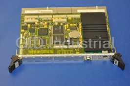


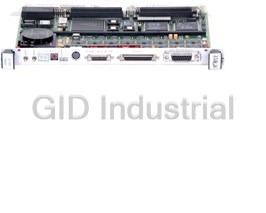


What they say about us
FANTASTIC RESOURCE
One of our top priorities is maintaining our business with precision, and we are constantly looking for affiliates that can help us achieve our goal. With the aid of GID Industrial, our obsolete product management has never been more efficient. They have been a great resource to our company, and have quickly become a go-to supplier on our list!
Bucher Emhart Glass
EXCELLENT SERVICE
With our strict fundamentals and high expectations, we were surprised when we came across GID Industrial and their competitive pricing. When we approached them with our issue, they were incredibly confident in being able to provide us with a seamless solution at the best price for us. GID Industrial quickly understood our needs and provided us with excellent service, as well as fully tested product to ensure what we received would be the right fit for our company.
Fuji
HARD TO FIND A BETTER PROVIDER
Our company provides services to aid in the manufacture of technological products, such as semiconductors and flat panel displays, and often searching for distributors of obsolete product we require can waste time and money. Finding GID Industrial proved to be a great asset to our company, with cost effective solutions and superior knowledge on all of their materials, it’d be hard to find a better provider of obsolete or hard to find products.
Applied Materials
CONSISTENTLY DELIVERS QUALITY SOLUTIONS
Over the years, the equipment used in our company becomes discontinued, but they’re still of great use to us and our customers. Once these products are no longer available through the manufacturer, finding a reliable, quick supplier is a necessity, and luckily for us, GID Industrial has provided the most trustworthy, quality solutions to our obsolete component needs.
Nidec Vamco
TERRIFIC RESOURCE
This company has been a terrific help to us (I work for Trican Well Service) in sourcing the Micron Ram Memory we needed for our Siemens computers. Great service! And great pricing! I know when the product is shipping and when it will arrive, all the way through the ordering process.
Trican Well Service
GO TO SOURCE
When I can't find an obsolete part, I first call GID and they'll come up with my parts every time. Great customer service and follow up as well. Scott emails me from time to time to touch base and see if we're having trouble finding something.....which is often with our 25 yr old equipment.
ConAgra Foods