

 Manufacturers
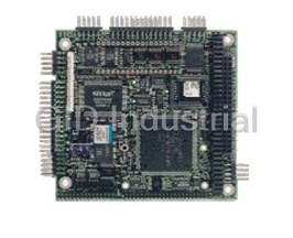
DIGITAL LOGIC MSM386SN4
Description
Digital Logic MSM386SN4 CPU Board - PC/104 Powerful ELAN310 CPU with 386 core SBC with 4 MB DRAM, without VGA/LCD, -25C to +70C Burn-In proofed, 33MHz
Part Number
MSM386SN4
Price
Request Quote
Manufacturer
DIGITAL LOGIC
Lead Time
Request Quote
Category
EMBEDDED COMPUTERS » PC/104 CPU
Datasheet

Extracted Text
TECHNICAL USER'S MANUAL FOR:
PC/104
MSM386SN/SV
Nordstrasse 11/F
CH- 4542 Luterbach
Tel.: ++41 (0)32 681 58 00
Fax: ++41 (0)32 681 58 01
Email: support@digitallogic.com
Homepage: http://www.digitallogic.com
DIGITAL-LOGIC AG MSM386SV/SN Manual V3.2
COPYRIGHT 1995- 2001 BY DIGITAL-LOGIC AG
No part of this document may be reproduced, transmitted, transcribed, stored in a retrieval system, in any
form or by any means, electronic, mechanical, optical, manual, or otherwise, without the prior written permis-
sion of DIGITAL-LOGIC AG.
The software described herein, together with this document, are furnished under a license agreement and
may be used or copied only in accordance with the terms of that agreement.
ATTENTION:
All information in this manual and the product are subject to change without prior notice.
REVISION HISTORY:
Prod.-Serialnumber: Product BIOS Doc. Date/Vis: Modification:
From: To: Version Version Version Remarks, News, Attention:
550xxx10000 550xxx1yyyy V2.2 V0.9 10.96 FK Initial Version
V4.0 V2.0 03.97 FK IDE modifications, BIOS
V5.1 V2.4 07.97 FK V5.1 Mod.
V2.5 08.97 FK BIOS Download
V2.6 08.97 FK RTC Reset IMPORTANT !
V2.61 08.97 FK RS485 description
V2.62 09.97 FK DOC2000, Virusalert
V5.1A V2.63 10.97 FK MSM104J, V5.1A Mod., Jumper
V2.64 11.97 FK V3/V4 DLFFSFMT.EXE
V2.74 03.98 SL FFS & Down.exe revision
V1.40B V2.75 03.98 JM Layout, detailed corrections
V2.76 03.98 JM POD-Code Table added
V2.77 03.98 SL FFS revision
V2.78 05.98 SL J35, J36 COM1 485 / TTL add
descr.
V2.79 08.98 JM Configuration table corrected
V2.80 11.98 FK Timer Adr. kor. page 32
V5.1A V1.41 V2.81b 01.99 JM Maintenance update
V1.41 V2.90 02.99 FK Y2K, BIOS-Hist, Address-MAP’s
V1.42 V2.91 03.99 FK New Download Tools
V2.92 03.99 JM Thermoscan pics added
V2.93 03.99 JM Related APP-NOTES
V2.94 04.99 FK Filter applications
V1.43 V2.95 05.99 JM Default chipset values
V2.96 10.99 FK Programming WatchDOG
V2.97 11.99 FK Comments in Chap.6, 4.3.2.
V2.98 01.00 STP Com 3 to Com 1 example added
V5.1A V1.43 V2.99 02.00 STP LPT- EPP sample added
V5.1A V1.43 V3.0 03.2000 STP Minor corrections
V5.1b V1.43 V3.1 10.2000 STP New address and logo, etc
V5.1b V1.44 V3.2 03.2001 STP Minor corrections
2
DIGITAL-LOGIC AG MSM386SV/SN Manual V3.2
READ CHAPTER 2.7 TO UNDERSTAND THE ELAN300 INCOMPATIBILITIES COMPARED TO THE
STANDARD PC-AT DESIGN !
Product Registration:
Please register your product at:
http://www.digitallogic.com -> SUPPORT -> Product Registration
After registration, you will receive driver & software updates, errata information, customer information and
news from DIGITAL-LOGIC AG products automatically.
3
DIGITAL-LOGIC AG MSM386SV/SN Manual V3.2
Table of Contents
1 PREFACE............................................................................................................. 7
1.1 Disclaimer ................................................................................................................................ 7
1.2 Technical Support ................................................................................................................... 7
1.3 Limited Warranty ..................................................................................................................... 8
2 OVERVIEW .......................................................................................................... 9
2.1 Standard Features................................................................................................................... 9
2.2 Unique Features ...................................................................................................................... 9
2.3 MSM386SV/SN Block Diagram............................................................................................ 10
2.4 MSM386SV/SN Specifications.............................................................................................. 11
2.5 Thermoscan ........................................................................................................................... 14
2.6 Ordering Codes ..................................................................................................................... 15
2.7 Incompatibilities or Warnings for the ELAN300/310.......................................................... 15
2.8 Related Application Notes....................................................................................................16
2.9 BIOS History .......................................................................................................................... 16
2.10 This product is “YEAR 2000 CAPABLE” ........................................................... 17
2.11 Mechanical dimensions ........................................................................................................ 18
2.12 RTC - Reset / Battery IMPORTANT INFORMATION........................................................... 19
2.13 High frequency radiation (to meet EN55022)...................................................................... 20
3 PC/104 BUS SIGNALS ...................................................................................... 21
4 DETAILED SYSTEM DESCRIPTION................................................................. 24
4.1 Power Requirements............................................................................................................. 24
4.1.1 Powersave Modes............................................................................................................24
4.2 CPU, Board and RAMs..........................................................................................................25
4.2.1 CPU of this MICROSPACE Product ................................................................................ 25
4.2.2 Numeric Coprocessor ...................................................................................................... 25
4.2.3 DRAM Memory................................................................................................................. 25
4.3 Interface.................................................................................................................................. 25
4.3.1 Keyboard AT-compatible and PS/2 Mouse...................................................................... 25
4.3.2 Line Printer Port LPT1...................................................................................................... 26
4.3.3 Serial Ports COM1-COM2-COM3.................................................................................... 27
4.3.4 Serial Ports RS485 on COM1 .......................................................................................... 28
4.3.5 Floppy Disk Interface ....................................................................................................... 28
4.3.6 Speaker Interface............................................................................................................. 29
4.4 Controllers ............................................................................................................................. 30
4.4.1 Interrupt Controllers ......................................................................................................... 30
4.5 Timers and Counters ............................................................................................................ 30
4.5.1 Programmable Timers...................................................................................................... 30
4.5.2 Battery Backed Clock (RTC)............................................................................................ 31
4.5.3 Watchdog ......................................................................................................................... 31
4.5.4 Watchdog Programming example.................................................................................... 31
4.6 BIOS........................................................................................................................................ 32
4.6.1 ROM-BIOS Sockets ......................................................................................................... 32
4.6.1.1 Standard BIOS ROM................................................................................................................. 32
4.6.2 EEPROM Memory for Setup............................................................................................ 33
4.6.3 BIOS CMOS Setup .......................................................................................................... 34
4.6.4 CMOS Setup Harddisk List .............................................................................................. 34
4.6.5 CMOS RAM Map ............................................................................................................. 35
4.6.6 Default chipset values...................................................................................................... 41
4.6.7 Harddisk PIO Modes ........................................................................................................ 41
4
DIGITAL-LOGIC AG MSM386SV/SN Manual V3.2
4.6.8 EEPROM saved CMOS Setup......................................................................................... 42
4.7 Download the VGA-BIOS and the CORE-BIOS.................................................................. 43
4.7.1 VGA- BIOS Download Function....................................................................................... 44
4.8 Memory / I/O Map................................................................................................................... 45
4.8.1 System I/O map ............................................................................................................... 46
4.8.2 BIOS-Variable-Segment................................................................................................... 61
4.8.2.1 Compatibility Service Table...................................................................................................... 67
4.8.2.2 System Configuration Parameter Table.....................................................................................68
4.9 VGA (only on MSM386SV Boards)....................................................................................... 69
4.9.1 VGA/LCD BIOS Support .................................................................................................. 72
4.9.2 Driver Resolutions and File names .................................................................................. 73
4.9.2.1 Windows.................................................................................................................................... 73
4.10 Keymatrix ............................................................................................................................... 74
4.10.1 Define a Keymatrix........................................................................................................... 74
4.10.2 Store the Keymatrix into the EEPROM ............................................................................ 74
4.10.3 Read DISK-File and store to the EEPROM-Matrix ......................................................... 74
4.10.4 Old step by step version for storing the values to another board .................................... 75
4.11 Character LCD Interface ....................................................................................................... 76
4.11.1 Character LCDs ............................................................................................................... 76
4.11.2 Two 4 Bit Character LCD with the HD44780 Controller................................................... 77
4.11.3 One 8 Bit Character LCD with the HD44780 Controller................................................... 77
4.11.4 CPU Bus interfaced DOT-Matrix LCDs............................................................................ 78
4.11.5 8 Bit Dot-Matrix LCD with the HD61830 Controller.......................................................... 79
4.11.6 8 Bit DOT-Matrix LCD with the T6963C Controller .......................................................... 80
5 DESCRIPTION OF THE CONNECTORS........................................................... 81
6 JUMPER LOCATIONS ON THE BOARD .......................................................... 90
6.1 The Jumpers on this MICROSPACE Product ..................................................................... 90
6.1.1 Jumper locations front side .............................................................................................. 92
6.1.2 Jumper locations rear side............................................................................................... 93
7 LED CRITERIONS: ............................................................................................ 94
8 CABLE INTERFACE.......................................................................................... 95
8.1 The harddisk cable 44pins ................................................................................................... 95
8.2 The COM 1/2 serial interface cable...................................................................................... 96
8.3 The printer interface cable (P4)............................................................................................ 97
8.4 The micro floppy interface cable ......................................................................................... 98
9 SPECIAL PERIPHERALS, CONFIGURATION.................................................. 99
9.1 Special peripherals................................................................................................................ 99
9.1.1 Multifunction Latch ........................................................................................................... 99
9.2 The Special Function Interface SFI...................................................................................... 99
9.2.1 EEPROM Functions: ........................................................................................................ 99
9.2.2 Watchdog functions:....................................................................................................... 101
9.2.3 INT15 Information: ......................................................................................................... 101
9.3 The Flashdisk....................................................................................................................... 102
9.3.1 Which Flashdisk Systems need a Flash-File-System.................................................... 102
9.3.2 Usable DOS size of a Flash-File-System....................................................................... 102
9.3.3 Used Memory Window on the PC.................................................................................. 103
9.3.4 Access and Data Integrity of the Flashdisk Technologies ............................................. 103
9.3.5 Installing the IDE-Flashdrives ........................................................................................ 103
9.3.5.1 Enabling and Formatting IDE-Flashdrives .............................................................................. 103
9.3.6 Installing the DIGITAL-LOGIC Flashdisk Module .......................................................... 104
9.3.6.1 Enabling and formatting the Flashdisk Module....................................................................... 104
9.3.7 Installing the flashdevice 29F040................................................................................... 105
9.3.7.1 Enabling and formatting the 29F040 flashdevice .................................................................... 105
5
DIGITAL-LOGIC AG MSM386SV/SN Manual V3.2
9.3.8 Installing the DOC2000 (M-System) .............................................................................. 106
9.3.8.1 Enabling and formatting of the DOC2000 (M-System)........................................................... 106
9.4 The Powersave Functions.................................................................................................. 108
9.4.1 Hardware controlled suspend/resume Function ............................................................ 108
9.4.2 Software controlled Power Management Functions ...................................................... 108
9.4.3 The different Powermodes............................................................................................. 108
9.4.4 Software controlled Powermode Switching.................................................................... 109
10 BUILDING A SYSTEM ..................................................................................... 110
10.1 Starting up the System ....................................................................................................... 110
11 THE POD-ERRORS ......................................................................................... 111
12 THE BIOS HARDDISK LIMITATIONS ............................................................ 113
13 INDEX............................................................................................................... 121
6
DIGITAL-LOGIC AG MSM386SV/SN Manual V3.2
1 PREFACE
This manual is for integrators and programmers of systems based on the MICROSPACE card family. It con-
tains information on hardware requirements, interconnections, and details of how to program the system.
The specifications given in this manual were correct at the time of printing; advances mean that some may
have changed in the meantime. If errors are found, please notify DIGITAL-LOGIC AG at the address shown
on the title page of this document, and we will correct them as soon as possible.
1.1 Disclaimer
DIGITAL-LOGIC AG makes no representations or warranties with respect to the contents of this manual and
specifically disclaims any implied warranty of merchantability or fitness for any particular purpose. DIGITAL-
LOGIC AG shall under no circumstances be liable for incidental or consequential damages or related ex-
penses resulting from the use of this product, even if it has been notified of the possibility of such damage.
DIGITAL-LOGIC AG reserves the right to revise this publication from time to time without obligation to notify
any person of such revisions. If errors are found, please contact DIGITAL-LOGIC AG at the address listed on
the title page of this document.
1.2 Technical Support
1. Contact your local DIGITAL-LOGIC Technical Support in your country first !
2. Use the Internet Support Request form at http://www.digitallogic.com -> Support -> Support Request
Form
3. Send a FAX or an E-mail to DIGITAL-LOGIC AG with a description of your problem.
DIGITAL-LOGIC AG
smartModule DesignIn Center
Nordstr. 11/F
CH-4542 Luterbach (SWITZERLAND)
Fax: ++41 32 681 58 01
E-Mail: support@digitallogic.com
Internet www.digitallogic.com
� Support requests will only be accepted with detailed information of the product (BIOS-, Board- Version) !
7
DIGITAL-LOGIC AG MSM386SV/SN Manual V3.2
1.3 Limited Warranty
DIGITAL-LOGIC AG warrants the hardware and software products it manufactures and produces to be free
from defects in materials and workmanship for one year following the date of shipment from DIGITAL-LOGIC
AG, Switzerland. This warranty is limited to the original purchaser of product and is not transferable.
During the one year warranty period, DIGITAL-LOGIC AG will repair or replace, at its discretion, any defec-
tive product or part at no additional charge, provided that the product is returned, shipping prepaid, to
DIGITAL-LOGIC AG. All replaced parts and products become property of DIGITAL-LOGIC AG.
Before returning any product for repair, customers are required to contact the company.
This limited warranty does not extend to any product which has been damaged as a result of accident, mis-
use, abuse (such as use of incorrect input voltages, wrong cabling, wrong polarity, improper or insufficient
ventilation, failure to follow the operating instructions that are provided by DIGITAL-LOGIC AG or other con-
tingencies beyond the control of DIGITAL-LOGIC AG), wrong connection, wrong information or as a result of
service or modification by anyone other than DIGITAL-LOGIC AG. Neither, if the user has not enough
knowledge of these technologies or has not consulted the product manual or the technical support of
DIGITAL-LOGIC AG and therefore the product has been damaged.
Except, as expressly set forth above, no other warranties are expressed or implied, including, but not limited
to, any implied warranty of merchantability and fitness for a particular purpose, and DIGITAL-LOGIC AG ex-
pressly disclaims all warranties not stated herein. Under no circumstances will DIGITAL-LOGIC AG be liable
to the purchaser or any user for any damage, including any incidental or consequential damage, expenses,
lost profits, lost savings, or other damages arising out of the use or inability to use the product.
8
DIGITAL-LOGIC AG MSM386SV/SN Manual V3.2
2 OVERVIEW
2.1 Standard Features
The MICROSPACE PC/104 is a miniaturized modulear device incorporating the major elements of a PC/AT
compatible computer. It includes standard PC/AT compatible elements, such as:
- Powerful ELAN310 CPU with 386 core
-BIOS ROM
- DRAM 2 or 4MBytes 70ns
-Timers
-DMA
- Real-time clock with CMOS-RAM and battery buffer
- LPT1 parallel port
- COM2, COM3 serial port RS232
- COM1 serial port with RS485
- Speaker interface
- AT-keyboard interface or PS/2-keyboard interface
- Keymatrix 8 x 16
- Floppy disk interface
- AT-IDE harddisk interface
- VGA/LCD video interface (only on MSM386SV boards)
- PC/104 embedded BUS
- PS/2 mouse interface
2.2 Unique Features
The MICROSPACE MSM386SV/SN includes all standard PC/AT functions plus unique DIGITAL-LOGIC AG
enhancements, such as:
- Flashdisk 512k - 8MByte
- SVGA/LCD interface
- Low power, 1 watt 3.3V CPU
- Single 5 volt supply
- WatchDog with Power-fail
- EEPROM for setup and configuration
- UL approved parts
- Onboard mounting of the MSFLASH-Drive with 4 or 10MByte
- Onboard keymatrix controller
9
DIGITAL-LOGIC AG MSM386SV/SN Manual V3.2
2.3 MSM386SV/SN Block Diagram
Accu
RTC
Speaker
DRAM
ELAN310
2, 4 MByte
386CPU
COM1
(RS485 LTC485)
16Bit
3
16Bit Data + 24Bit Address
5
ISA-BUS
PC/104 BIOS Super I/O KB Flashdisk
37C666
Bus 128kByte Mouse 0 - 8 MB
MAX211 MAX211
FD IDE LPT1 COM3 COM2 KB Mouse
ISA-BUS
Key Matrix
8Bit
Video RAM
EEPROM
Char./L LCD/VGA Con- Watchdog
1 MByte
2kByte
CD troller 65540
LCD CRT
8Bit
10
DIGITAL-LOGIC AG MSM386SV/SN Manual V3.2
2.4 MSM386SV/SN Specifications
CPU:
CPU 386:
AMD 310�
Mode: Real / Protected
Compatibility: 8086 - 80386
Word Size: 16 Bits
Physical Addressing: 24 lines
Virtual Addressing: 16 MBytes
Clock Rates: 25, 33MHz selectable
Socket Standard: directly soldered onboard
Math. Coprocessor:
not available on AMD-ELAN310
Power Management:
available clock switching, sleep, possible controlled power-up,
inactivity-auto powerdown
DMA:
8237A comp. 4 channels 8 Bits
3 channels 16 Bits
Interrupts:
8259 comp. 8 + 7 levels
PC compatible
Timers:
8254 comp. 3 programmable counter/timers
Memory:
DRAM 2 or 4 MByte directly soldered
Video only on SV boards:
Controller: 65545 from C&T
BUS: ISA 16Bit
Enhanced BIOS: VGA / LCD BIOS
Memory: VRAM onboard: 1MByte
CRT-Monitor: VGA, SVGA up to 768 x 1024 pixels 16/256 colors
Flatpanel: TFT: 640 x 480 with 8/16/256 colors
STN: 640 x 480 monochrome
STN: 640 x 480 with 256 colors
Plasma: up to 1280 x 1024
EL: 640 x 350 , 640 x 480, 768 x 1024 pixels
Controller Modes: CRT only; Flatpanel only or simultaneous CRT and Flatpanel
LCD-BIAS: not available onboard
Drivers: Windows
Mass Storage:
FD: Floppy disk interface, for max. 1 floppy with 26pin connector
HD: IDE interface, AT - Type, for max. 2 harddisks, 44pin connector, for
1.3, 1.8 and 2.5" harddisk with 44pin IDE
11
DIGITAL-LOGIC AG MSM386SV/SN Manual V3.2
Sockets SSD:
1st socket: READ/WRITE/BOOTABLE Flashdiskmodule 512kByte - 8MByte
IDE: MSFLASH-Drive 4MB or 10MB onboard mountable
Standard AT Interfaces:
Serial: Name FIFO IRQs Addr. Standard
COM1 no IRQ4 3F8 TTL / RS485 (ltc485)
COM2 yes IRQ3 2F8 RS232C
COM3 yes IRQ4/5/10 3E8 RS232C
COM3 is default on IRQ10. It may be jumpered to IRQ 4 or IRQ5.
(Baudrates: 50 - 115 KBaud programmable)
Parallel: LPT1 printer interface mode: SPP (output only) , EPP (bidirectional)
Keyboard: AT or PS/2 –keyboard
Keymatrix 8 x 16
Mouse: AT or PS/2
Speaker: 0.1 W output drive
RTC: integrated into the ELAN310, RTC with CMOS-RAM 128Byte
Backup current:
<50 μA
Battery: 3.6V 70mAh Ni-Cd or NiMh or external
Supervisory:
Watchdog: LTC1232 with power-fail detection, strobe time max. 1sec.
BUS:
PC/104 IEEE-996 standard bus, buffered with 24mA
Clock: 8 MHz or programmable
Peripheral Extension:
with PC/104 BUS
Power Supply:
Working:
5 Volts ± 5%
Power Rise Time:
>100μs (0V --> 4,75V)
Current: SV: 740mA nominal SN: 400mA nominal
SV: 410mA in sleep mode SN: 210mA in sleep mode
Physical Characteristics:
Dimensions: Length: 90 mm
Depth: 96 mm
Height: 20 mm
Weight: SV: 90gr / SN: 70gr
PCB Thickness: 1.6 mm / 0.0625 inches nominal
PCB Layer: 8 with separate ground and VCC plane for low noise
12
DIGITAL-LOGIC AG MSM386SV/SN Manual V3.2
Operating Environment:
Relative Humidity: 5 - 90% non condensing
Vibration: 5 to 2000 Hz
Shock: 10 G
Temperature: Operating: Standard version: -25°C to +70°C *)
Extended version: -40°C to +85°C T.B.A.
Storage: -55°C to +85 °C *)
*) with onboard backupbattery, only +60°C peak are allowed.
EMI / EMC (IEC1131-2 refer MIL 461/462):
ESD Electro Static Discharge: IEC 801-2, EN55101-2, VDE 0843/0847 Part 2
metallic protection needed
separate Ground Layer included
15 kV single peak
REF Radiated Electromagnetic Field: IEC 801-3, VDE 0843 Part 3, IEC770 6.2.9.
not tested
EFT Electric Fast Transient (Burst): IEC 801-4, EN50082-1, VDE 0843 Part 4
250V - 4kV, 50 ohms, Ts=5ns
Grade 2: 1KV Supply, 500 I/O, 5Khz
SIR Surge Immunity Requirements: IEC 801-5, IEEE587, VDE 0843 Part 5
Supply: 2 kV, 6 pulse/minute
I/O: 500 V, 2 pulse/minute
FD, CRT: none
High-frequency radiation: EN55022
Compatibility:
MSM386SV/SN: mechanically compatible to our MSMx86 Boards and to all other
PC/104 boards
Any information is subject to change without notice.
13
DIGITAL-LOGIC AG MSM386SV/SN Manual V3.2
2.5 Thermoscan
Product: MSM386SV4 Scan time: 60min.
14
DIGITAL-LOGIC AG MSM386SV/SN Manual V3.2
2.6 Ordering Codes
MSM386SV2 with 2 MB DRAM, with VGA/LCD -25°C to +70°C BurnIn proofed, 33MHz
MSM386SV4 with 4 MB DRAM, with VGA/LCD -25°C to +70°C BurnIn proofed, 33MHz
MSM386SN2 with 2 MB DRAM, without VGA/LCD -25°C to +70°C BurnIn proofed, 33MHz
MSM386SN4 with 4 MB DRAM, without VGA/LCD -25°C to +70°C BurnIn proofed, 33MHz
-E48 Extended temperature range -40°C to +85°C BurnIn proofed, 25MHz
MSFLASH4 Flashdrive 4 MB on IDE interface
MSFLASH10 Flashdrive 10 MB on IDE interface
MSM3/486V/-CK Cablekit for MSM386V/486V/486DX
MSSD-F2S0 Flashdisk Module 2 MB
MSSD-F4S0 Flashdisk Module 4 MB
MSSD-F6S0 Flashdisk Module 6 MB
MSSD-F8S0 Flashdisk Module 8 MB
MSSD-F0S1 SRAM Module 1 MB
MSFLA-05DL Flash Device 29F040 with 512kB DIL32
2.7 Incompatibilities or Warnings for the ELAN300/310
1. The ELAN300 has an internal PCMCIA controller, the external must have an alternative address
The internal PCMCIA controller operates at the address 3E0h / 3E1h. Using the MSM386SV board with an
MSM104J PCMCIA board needs the following modification on the MSM104J board:
J18 = 2-3 and J14 = 1-2 -> Base Address is now 3E2h
The MMCD.SYS receives the option /B:3E2h
Boot option for selecting the Index Base Addresses on the MSM104J board:
J18 J14:
INTR: SPKROUT: Index Base: I/O Address: Comment:
1-2 (VCC) 1-2 (VCC) 00h 3E0h/3E1h DEFAULT
1-2 (VCC) 2-3 (GND) 80h 3E0h/3E1h
2-3 (GND) 1-2 (VCC) 00h 3E2h/3E3h (needed on ELAN300/400 boards)
2-3 (GND) 2-3 (GND) 80h 3E2h/3E3h
15
DIGITAL-LOGIC AG MSM386SV/SN Manual V3.2
2.8 Related Application Notes
# Description
38 ELAN310 with IDE
39 ELAN310 IRQ for COM-Ports
44 Akku as a backup power for the RTC data
45 COM3 to COM1
52 EPP Mode for MSM386SV/SN
54 Problem between powerdown and int COM disable
55 All you wish to know about COM on MSM386SV/SN
57 PCMCIA Controller of the ELAN or VADEM
65 MSM386SV and MSMJ104/D, SYSCLK-Loads
78 Several versions of the FFS format
80 High frequency Radiation (to meet EN55022)
84 Power consumption on Pentium / any other boards with at-
tached drives (HDD, CD)
� Application Notes are availble at http://www.digitallogic.com ->support, or on any Application CD from
DIGITAL-LOGIC.
2.9 BIOS History
Version: Date: Status: Modifications:
1.40 Juni 97 released Basic BIOS
1.41 Aug. 98 released Y2K support added, FFS V6.0
1.42 Feb. 99 released C-Segment Shadow programmable
Wait Time for ALT-CTRL-S longer
FFS V7.02
1.43 May 99 released Boot with video shadow
FFS 7.02 read & write, read only correction
1.44 27.10.2000 released FFS 7.03, EEPROM support added
16
DIGITAL-LOGIC AG MSM386SV/SN Manual V3.2
2.10 This product is “YEAR 2000 CAPABLE”
This DIGITAL-LOGIC product is “YEAR 2000 CAPABLE”. This means, that upon installation, it accurately
stores, displays, processes, provides and/or receives date data from, into, and between 1999 and 2000, and
the 20. and 21. centuries, including leap year calculations, provided that all other technology used in combi-
nation with said product properly exchanges date data with it. DIGITAL-LOGIC makes no representation
about individual components within the product should be used independently from the product as a whole.
You should understand that DIGITAL-LOGIC’s statement that an DIGITAL-LOGIC product is “YEAR 2000
CAPABLE” means only that DIGITAL-LOGIC has verified that the product as a whole meet this definition
when tested as a stand-alone product in a test lab, but dies not mean that DIGITAL-LOGIC has verified that
the product is “YEAR 2000 CAPABLE” as used in your particular situation or configuration. DIGITAL-LOGIC
makes no representation about individual components, including software, within the product should they be
used independently from the product as a whole.
DIGITAL-LOGIC customers use DIGITAL-LOGIC products in countless different configurations and in con-
junction with many other components ans systems, and DIGITAL-LOGIC has no way to test wheter all those
configurations and systems will properly handle the transition to the year 2000. DIGITAL-LOGIC encourages
its customers and others to test whether their own computer systems and products will properly handle the
transition to the year 2000.
The only proper method of accessing the date in systems is indirectly from the Real-Time-Clock via the
BIOS. The BIOS in DIGITAL-LOGIC computerboards contain a century checking and maintenance feature
the checks the laest two significant digits of the year stored in the RTC during each BIOS request (INT 1A) to
read the date and, if less than ‘80’ (i.e. 1980 is the first year supported by the PC), updates the century byte
to ‘20’. This feature enables operating systems and applications using BIOS date/time services to reliably
manipulate the year as a four-digit value.
17
DIGITAL-LOGIC AG MSM386SV/SN Manual V3.2
2.11 Mechanical dimensions
Top View MSM386SV V5.1A
All Dimensions are in millimeters, +/-0.1
2.5
20.3
7.5
6.0
8.9 5.1
J15 - COM2
5.1
3.1
1.3
J10 - VGA/LCD
J11 - FDC - MOLEX
o3.0HOLE TYP.
2.0Typ.
22.3
2.5Typ.:VGA/LCD;COM1,2;LPT1;Keyb;Power
2.5Typ.
2.0Typ.:HD;FDC
U26
95.8
68.5
U6 - CPU
U17 - BIOS
30.4
12.3
12.6
Norm PC104
J2 - Power
5.1
6.4
2.6
1.6
21.6
80
5.1
90.2
18
2.0Typ.
2.0Typ.
J6 - Keymatrix
J17 - HD
J9 - Character LCD
2.5Typ.
J3 - Keyb J14 - COM1
J16 - LPT1
DIGITAL-LOGIC AG MSM386SV/SN Manual V3.2
2.12 RTC - Reset / Battery IMPORTANT INFORMATION
The ELAN3x0 device includes a built-in 146818A compatible realtime clock (RTC) with 114 bytes of SRAM.
The RTC SRAM is designed to hold configuration data and to maintain accurate time and date when the rest
of the system is powered down. This state is called the MICRO POWER OFF mode. MICRO POWER OFF
mode allows the system to conserve battery power by removing all power to all system components and the
ELAN300 device except for the AVCC and the VCC pins. Maintaining power on these pins allows the RTC to
remain powered up, preventing the system from losing ist configuration, time and data data. This feature al-
lows an AT-compatible system to be implemented without using an external RTC device.
REAL TIME CLOCK
The ELAN300 is designed to operate properly, while in MICRO POWER OFF mode, at voltages all the way
down to 2.4V with the power consumption of around 40μA. Any source below 2.4V will not guarantee proper
functionality, which could mean the loss of system configuration data, date and time.
BACKUP BATTERY
The MICRO POWER OFF mode of the ELAN300 allows the main system power source to be turned off and
a backup source to be switched in to maintain power for the RTC.
IMPORTANT POINT 1:
If a RTC backup battery is installed on the system , while the main power is off, the ELAN300 will come up in
an undefined state causing power consumption in the mA range which could drain the backup battery!
There are also IRQ accessing errors possible.
1. Solution:
The backup battery must be installed after the system is powered with the main source, and is fully working.
Therefore close jumper J5 only if the main source is already on.
IMPORTANT POINT 2:
If the RTC backup battery goes under 2.4V the MICRO POWER OFF mode will be stopped, and the system
will loose all configuration from the RTC. If the system main power is switched on, the configuration data will
be copied form the EEPROM to the RTC SRAM.
If the backup battery is not fully empty (in the range of 0.4V to 1.8V), the system will not come up when the
main power is on, because the ELAN is in an undefined state. In this case, the backup battery must be fully
interrupted for a very short time (by opening the J5 jumper). After the system has started, the jumper could
be closed and the system should be powered until the backup battery is fully charged.
2.A solution:
In every design, using a backup battery for the RTC (also the onboard accu), install a reset switch with a ca-
ble to jumper J5. This switch should be placed in the rearside of the case, and should be activated only with
a small pen. This prevents from accidently resetting the RTC, if the system if powered off.
Indicate in your operating manual, that the system could hang, if the RTC battery is nearly fully unloaded.
Only in this case, this RTC-Reset switch must be pressed, to interrupt J5 for a short time until the main
power is on. All palmtop computers have exactly the same RTC reset switch!
2.B solution:
If you do not need an RTC date and time, dismount the backup battery and start every bootup from the
EEPROM configuration values. In this case, nothing must be observed.
19
DIGITAL-LOGIC AG MSM386SV/SN Manual V3.2
2.13 High frequency radiation (to meet EN55022)
Since the PC/104 CPU modules are very high integrated embedded computers, no peripheral lines are pro-
tected against the radiation of high frequency spectrum. To meet a typical EN55022 requirement, all periph-
erals, they are going outside of the computer case, must be filtered externaly.
Typical signals, they must be filtered:
Keyboard: KBCLK, KBDATA, VCC
Mouse: MSCLK, MSDATA, VCC
COM1/2/3/4: All serial signals must be filtered
LPT: All parallel signals must be filtered
CRT: red,blue,green, hsynch, vsynch must be filtered
Typical signals, they must not be filtered, since they are internaly used:
IDE: connected to the harddisk
Floppy: connected to the floppy
LCD: connected to the internal LCD
1. For peripheral cables:
Use for all DSUB connector a filtered version. Select carefully the filter specifications.
Place the filtered DSUB connector directly frontside and be sure that the shielding makes
a good contact with the case.
9pin DSUB connector from AMPHENOL: FCC17E09P 820pF
25pin DSUB connector from AMPHENOL: FCC17B25P 820pF
2. For stackthrough applications:
Place on each peripheral signal line, they are going outside, a serial inductivity and
after the inductivity a capacitor of 100pF to 1000pF to ground.
In this case, no filtered connectors are needed. Place the filter directly under or
behind the onboard connector.
Serial Inductivity: TDK HF50ACB321611-T 100MHz, 500mA, 1206 Case
Ground capacitor: Ceramic Capacitor with 1000pF
Power supply:
Use a current compensated dualinductor on the 5V supply e.g.
SIEMENS B82721-K2362-N1 with 3.6A , 0.4mH
20
DIGITAL-LOGIC AG MSM386SV/SN Manual V3.2
3 PC/104 BUS SIGNALS
AEN, output
Address Enable is used to degate the microprocessor and other devices from the I/O channel to allow DMA
transfers to take place. low = CPU Cycle , high = DMA Cycle
BALE, output
Address Latch Enable is provided by the bus controller and is used on the system board to latch valid ad-
dresses and memory decodes from the microprocessor. This signal is used so that devices on the bus can
latch LA17..23. The SA0..19 address lines latched internally according to this signal. BALE is forced high
during DMA cycles.
/DACK[0..3, 5..7], output
DMA Acknowledge 0 to 3 and 5 to 7 are used to acknowledge DMA requests (DRQO through DRQ7). They
are active low. This signal indicates that the DMA operation can begin.
DRQ[0..3, 5..7], input
DMA Requests 0 through 3 and 5 through 7 are asynchronous channel requests used by peripheral devices
and the I/O channel microprocessors to gain DMA service (or control of the system). A request is generated
by bringing a DRQ line to an active level. A DRQ line must be held high until the corresponding DMA Re-
quest Acknowledge (DACK/) line goes active. DRQO through DRQ3 will perform 8-Bit DMA transfers; DRQ5-
7 are used for 16 accesses.
/IOCHCK, input
IOCHCK/ provides the system board with parity (error) information about memory or devices on the I/O
channel. low = parity error, high = normal operation
IOCHRDY, input
I/O Channel Ready is pulled low (not ready) by a memory or I/O device to lengthen I/O or memory cycles.
Any slow device using this line should drive it low immediately upon detecting its valid address and a Read
or Write command. Machine cycles are extended by an integral number of one clock cycle (67 nanosec-
onds). This signal should be held in the range of 125-15600nS. low = wait, high = normal operation
/IOCS16, input
I/O 16 Bit Chip Select signals the system board that the present data transfer is a 16-Bit, 1 wait-state, I/0 cy-
cle. It is derived from an address decode. /IOCS16 is active low and should be driven with an open collector
(300 ohm pull-up) or tri-state driver capable of sinking 20mA. The signal is driven based only on SA15-SAO
(not /IOR or /IOW) when AEN is not asserted. In the 8 Bit I/O transfer, the default transfers a 4 wait-state cy-
cle.
/IOR, input/output
I/O Read instructs an I/O device to drive its data onto the data bus. It may be driven by the system micro-
processor or DMA controller, or by a microprocessor or DMA controller resident on the I/O channel. This sig-
nal is active low.
/IOW, input/output
I/O Write instructs an I/O device to read the data on the data bus. It may be driven by any microprocessor or
DMA controller in the system. This signal is active low.
IRQ[ 3 - 7, 9 - 12, 14, 15], input
These signals are used to tell the microprocessor that an I/O device needs attention. An interrupt request is
generated when an IRQ line is raised from low to high. The line must be held high until the microprocessor
acknowledges the interrupt request.
/Master, input
This signal does not exist on the ELAN3xx designs.
/MEMCS16, input
MEMCS16 Chip Select signals the system board if the present data transfer is a 1 wait-state, 16-Bit, memory
cycle. It must be derived from the decode of LA17 through LA23. /MEMCS16 should be driven with an open
collector (300 ohm pull-up) or tri-state driver capable of sinking 2OmA.
21
DIGITAL-LOGIC AG MSM386SV/SN Manual V3.2
/MEMR input/output
These signals instruct the memory devices to drive data onto the data bus. /MEMR is active on all memory
read cycles. /MEMR may be driven by any microprocessor or DMA controller in the system. When a micro-
processor on the I/0 channel wishes to drive /MEMR, it must have the address lines valid on the bus for one
system clock period before driving /MEMR active. These signals are active low.
/MEMW, input/output
These signals instruct the memory devices to store the data present on the data bus. /MEMW is active in all
memory read cycles. /MEMW may be driven by any microprocessor or DMA controller in the system. When a
microprocessor on the I/O channel wishes to drive /MEMW, it must have the address lines valid on the bus
for one system clock period before driving /MEMW active. Both signals are active low.
OSC, output
Oscillator (OSC) is a high-speed clock with a 70 nanosecond period (14.31818 MHz). This signal is not syn-
chronous with the system clock. It has a 50% duty cycle. OSC starts 100μs after reset is inactive.
RESETDRV, output
Reset Drive is used to reset or initiate system logic at power-up time or during a low line-voltage outage. This
signal is active high. When the signal is active all adapters should turn off or tri-state all drivers connected to
the I/O channel. This signal is driven by the permanent Master.
/REFRESH, input/output
This signal does not exist on ELAN3xx designs (onboard pulled up to VCC).
SAO-SA19, LA17 - LA23 input/output
Address bits 0 through 19 are used to address memory and I/0 devices within the system. These 20 address
lines, allow access of up to 1MBytes of memory. SAO through SA19 are gated on the system bus when
BALE is high and are latched on the falling edge of BALE. LA17 to LA23 are not latched and addresses the
full 16 MBytes range. These signals are generated by the microprocessors or DMA controllers.
/SBHE, input/output
Bus High Enable (system) indicates a transfer of data on the upper byte of the data bus, XD8 through XD15.
16Bit devices use /SBHE to condition data-bus buffers tied to XD8 through XD15.
SD[O..15], input/output
These signals provide bus bits 0 through 15 for the microprocessor, memory, and I/0 devices. DO is the
least-significant Bit and D15 is the most significant Bit. All 8-Bit devices on the I/O channel should use DO
through D7 for communications to the microprocessor. The 16-Bit devices will use DO through D15.
/SMEMR input/output
These signals instruct the memory devices to drive data onto the data bus for the first MByte. /SMEMR is
active on all memory read cycles. /SMEMR may be driven by any microprocessor or DMA controller in the
system. When a microprocessor on the I/0 channel wishes to drive /SMEMR, it must have the address lines
valid on the bus for one system clock period before driving /SMEMR active. The signal is active low.
/SMEMW, input/output
These signals instruct the memory devices to store the data present on the data bus for the first MByte.
/SMEMW is active in all memory read cycles. /SMEMW may be driven by any microprocessor or DMA con-
troller in the system. When a microprocessor on the I/O channel wishes to drive /SMEMW, it must have the
address lines valid on the bus for one system clock period before driving /SMEMW active. Both signals are
active low.
SYSCLK, output
This is a 8 MHz system clock. It is a synchronous microprocessor cycle clock with a cycle time of 167 nano-
seconds. The clock has a 66% duty cycle. This signal should only be used for synchronization.
TC output
Terminal Count provides a pulse when the terminal count for any DMA channel is reached. Onboard from FD
used.
22
DIGITAL-LOGIC AG MSM386SV/SN Manual V3.2
/OWS, input
The Zero Wait State (/OWS) signal tells the microprocessor that it can complete the present bus cycle with-
out inserting any additional wait cycles.
12V +/- 5%
Used only for the flatpanel supply.
The Bus currents are:
Output Signals: IOH: IOL:
D0 - D16 12 mA 12 mA
A0 - A23 12 mA 12 mA
MR, MW, IOR, IOW, RES, ALE, AEN, C14 12 mA 12 mA
DACKx, DRQx, INTx, PSx, OPW 12 mA 12 mA
Output Signals: Logic Family: Voltage:
ABT-Logic ABT-Logic
Input Signals: ViH (min.) = 2.15 V Vil (max.) = 0.85 V
23
DIGITAL-LOGIC AG MSM386SV/SN Manual V3.2
4 DETAILED SYSTEM DESCRIPTION
This system has a system configuration based on the ISA architecture. Check the I/O and the Memory map
in this chapter.
4.1 Power Requirements
The power is connected through the PC/104 power connector; or the separate power connector on the
board. The supply uses only the +5 Volts and ground connection.
Warning: Make sure that the power plug is wired correctly before supplying power to the board!
4.1.1 Powersave Modes
MSM386SV/SN MSM486SV MSM486DX MSM486DX PCC-P5 PCC-P5
DRAM 4 8 16 16 16 16
3.3V Gen. linear linear linear switched linear switched
Fullspeed 33MHz 66MHz 100MHz 100MHz 166MHz 166MHz
at 5.0V 600mA 1000mA 1800mA 1300mA 4000mA 3000mA
Power 3W 5W 9W 6.5W 20W 15W
Ti, Sus, Sw Ti, Sus, Sw Ti, Sw Ti, Sw Ti Ti
↓ Powerdn
Low Speed 20MHz 33MHz 4MHz 4MHz 10MHz 10MHz
at 5.0V 450mA 800mA 850mA 800mA 2000mA 1800mA
Power 2W 4W 4.5W 4W 10W 9W
VGA,MAX on on on on on on
↓ Powerdn Ti, Sus, Sw Ti, Sus, Sw Ti, Sw Ti, Sw Ti Ti
↑ Powerup Ac, Res, Sw Ac,Res, Sw Ac, Res Ac, Res Ac Ac
Suspend 1MHz 1MHz
at 5.0V 160mA 180mA
Power 0.8W 0.9W
VGA off off
MAX211 off off
Ti, Sus, Sw Ti, Sus, Sw
↓ Powerdn
Ac, Res, Sw Ac,Res, Sw
↑ Powerup
Sleep 0MHz 0MHz 0MHz 0MHz
at 5.0V 140mA 160mA 600mA 600mA
VGA off off off off
MAX211 off off on on
Keyboard off off off off
↑ Powerup Res Res Res Res
In all powermodes, the program is resident in the refreshed DRAM!
Others: KBD = 10mA, Floppy = 10mA, HD = 300mA/10mA, Flashdisk = 1mA, VGA = ~300mA
Remarks: Ti 1s to 24h prog.=Timer controlled (modifiable in the CMOS-Setup)
Sus/Res 500ms = Suspend / Resume signal (hardware)
Sw 500ms = Software controlled, by programming a register
Ac 500ms = Activity, Keyboard pressed, Mouse, COMx,
24
DIGITAL-LOGIC AG MSM386SV/SN Manual V3.2
4.2 CPU, Board and RAMs
4.2.1 CPU of this MICROSPACE Product
Processor: Type: Clock: Landmark MHz: Landmark Units:
ELAN 310-B4 AMD 33 MHz 30 MHz 100
4.2.2 Numeric Coprocessor
Is not integrated in the ELAN 310 CPU.
4.2.3 DRAM Memory
Speed: 70ns
Size:
soldered onboard SOJ DRAMs
Bits: 16 Bit
Capacity: 2 or 4 MBytes
Bank: 1 or 2
4.3 Interface
4.3.1 Keyboard AT-compatible and PS/2 Mouse
J3 Pin Signal
Pin 1 Speaker out
Pin 2 Resume Input
Pin 3 Reset Input.
A mechanical pushbutton or an active
logic signal can drive the reset input. The
debounced input ignores input pulses less
than 1ms and is guaranteed to recognize
pulses of 20ms or grater.
Pin 4 VCC
Pin 5 Keyb. Data
Pin 6 Keyb. Clock
Pin 7 Ground
Pin 8 Ext. Battery
Pin 9 Mouse Clock (PS/2)
Pin 10 Mouse Data (PS/2)
25
DIGITAL-LOGIC AG MSM386SV/SN Manual V3.2
4.3.2 Line Printer Port LPT1
A standard bi-directional LPT port is integrated in the MICROSPACE PC.
Further information about these signals is available in numerous publications, including the IBM technical
reference manuals for the PC and AT computers and from some other reference documents.
The current is: IOH = 12 mA IOL = 24mA
The SMC 37C666 may be programmed with reset strap options in the following modes:
Parallel Port Address (default LPT1)
The jumpers are available since board version 5.1.
PCF1 (RTS1) R50 / J51 PCF0 (TXD1) J22 port address IRQ
low 1-2 low 2-3 disabled 7
low 1-2 high 1-2 PS2 3BCh 7
high 2-3 low 2-3 LPT1 378h
7
high 2-3 high 1-2 LPT2 278h 7
In order to make any changes the resistor must be wired to the other potential.
Parallel Port Mode (default normal)
The jumpers are available and the DACK7/DRQ7 are connected since board version 5.1!
ECPEN (MTR2) J53 PADCF (GAME) J52 port function
low 1-2 low 1-2 Standard Printer Port, output only
low 1-2 high 2-3 Enhanced Printer Port (EPP), bidirection
Extended Capabilities Printer Port (ECP)
high 2-3 low 1-2
high 2-3 high 2-3 ECP & EPP
ATTENTION:
If others than standard mode are used, check the BIOS-setup, that the “ INTERNAL LPT PORT” is disabled.
For EPP and ECP mode, the LPT port is using the DMA7 and the IRQ7.
26
DIGITAL-LOGIC AG MSM386SV/SN Manual V3.2
4.3.3 Serial Ports COM1-COM2-COM3
The serial channels are fully compatible with 16C550 UARTS. COM1 is the primary serial port, and is sup-
ported by the board's ROM-BIOS as the PC-DOS 'COM1' device. The secondary serial port is COM2; it is
supported as the 'COM2' device. In the BIOS Setup only COM1 is programmable. The COM2 and COM3 is
hardware defined.
Standard: COM 3/2: 37C666 (SMC): 2 x 16C550 compatible serial interfaces with RS232C
COM1: ELAN310: 1 x 16C450 compatible serial interface with RS485
Serial Port Connectors COM2, COM3
Pin Signal Name Function in/out DB25 Pin DB9 Pin
1 CD Data Carrier Detect in 8 1
2 DSR Data Set Ready in 6 6
3RXD Receive Data in 3 2
4 RTS Request To Send out 4 7
5 TXD Transmit Data out 2 3
6 CTS Clear to Send in 5 8
7 DTR Data Terminal Ready out 20 4
8 RI Ring Indicator in 22 9
9 GND Signal Ground 7 5
The serial port signals are compatible with the RS232C specifications.
The COM of the ELAN (default COM1)
ELAN port address IRQ
register int com disabled Disabled
register int com enabled COM1 3F8h
4
To make any changes the BIOS must be modified.
The internal UART is hardwired on the address of the COM1 and of the IRQ4. No other modification to other
addresses or IRQ numbers are possible.
The SMC 37C666 may be programmed with reset strap options in the following modes:
The first serial channel is in the ELAN controller (if enabled in the BIOS-Setup, always on COM1).
J14 = Second serial channel (default COM3)
S1CF1 (IDELO line) R45 S1CF0 (IDEHI line) R46 port address IRQ
low low Disabled 4, 5, 10
low (COM3) high COM3 3E8h 4, 5, 10
high low COM2 2F8h 4, 5, 10
high (COM1) high COM1 3F8h 4, 5, 10
In order to make any changes the resistor must be wired to the other potential. If the internal UART from the
ELAN300 is disabled (BIOS-Setup), J14 may be configured as COM1 (by setting wiring the R45 to Vcc in-
stead to GND).
In the future, the settings will be done by the CMOS- setup, and the new board version (V5.1) will use J54
instead of wiring the R45 (see also chapter 6).
J15 = Third serial channel (default COM2)
S2CF1 (DTR1 line) R53 S2CF0 (RTS2 line) R51 or J50 port address IRQ
low low Disabled 3
low high COM4 2E8h 3
high low COM1 3F8h 3
high high COM2 2F8h 3
In order to make any changes the resistor must be wired to the other potential.
27
DIGITAL-LOGIC AG MSM386SV/SN Manual V3.2
4.3.4 Serial Ports RS485 on COM1
The RS485 interface is controlled by the RTS/DTS outputs. The application must be able to control the
RS485 port correctly.
Function: Output: Input: RTS-Output DTS-Output Remarks:
RS485 RS485 = DE of the = RE/ of the LTC485
LTC485 (3FCh Bit0)
(3FCh Bit1)
RS485 Enabled Disabled 0 0 Transmit Data
RS485 Enabled Enabled 0 1 TxD & RxD, Loopback
RS485 Disabled Disabled 1 0 No Bus Access
RS485 Disabled Enabled 1 1 Receive only Data
4.3.5 Floppy Disk Interface
The onboard floppy disk controller and ROM-BIOS support one or two floppy disk drives in any of the stan-
dard PC-DOS and MS-DOS formats shown in the table.
Supported Floppy Formats
Capacity Drive size Tracks Data rate DOS version
1.2 MB 5-1/4" 80 500 KHz 3.0 - 6.22
720 K 3-1/2" 80 250 KHz 3.2 - 6.22
1.44 M 3-1/2" 80 500 KHz 3.3 - 6.22
Floppy Interface Configuration
The desired configuration of floppy drives (number and type) must be properly initialized in the board's
CMOS - configuration memory. This is generally done by using CTRL + ALT + 'S' at bootup time.
Floppy Interface Connector
The table shows the pinout and signal definitions of the board's floppy disk interface connector. It is identical
in pinout to the floppy connector of a standard AT. Note that, as in a standard PC or AT, both floppy drives
are jumpered to the same drive select: as the 'second' drive. The drives are uniquely selected as a result of a
swapping of a group of seven wires (conductors 10-16) that must be in the cable between the two drives.
The seven-wire swap goes between the computer board and drive 'A'; the wires to drive 'B' are unswapped
(or swapped a second time). The 26 pin high density (1mm pitch FCC) connector has only one drive and
motor select. The onboard jumper defines the drive A: or B:. Default is always A:.
Floppy Disk Interface Technology
We only support CMOS drives. That means that the termination resistors are 1 Kohm. 5 1/4“-drives are not
recommended (TTL interface).
The 26 pin connector: FFC/FPC 0.3mm thick 1.0mm (0.039") pitch (MOLEX 52030 Serie)
28
DIGITAL-LOGIC AG MSM386SV/SN Manual V3.2
Floppy Disk Interface connector
FD26: Pin Signal Name Function in/out
1VCC +5 volts
2 IDX Index Pulse in
3VCC +5 volts
4 DS2 Drive Select 2 out
5VCC +5 volts
6 DCHG Disk Change in
10 M02 Motor On 2 out
12 DIRC Direction Select out
14 STEP Step out
16 WD Write Data out
17 GND Signal grounds
18 WE Write Enable out
19 GND Signal grounds
20 TRKO Track 0 in
21 GND Signal grounds
22 WP Write Protect in
23 GND Signal grounds
24 RDD Read Data in
25 GND Signal grounds
26 HS Head Select out
4.3.6 Speaker Interface
One of the board's CPU device provides the logic for a PC compatible speaker port. The speaker logic signal
is buffered by a transistor amplifier, and provides approximately 0.1 watt of audio power to an external 8 ohm
speaker. Connect the speaker between VCC and speaker output to have no quiescient current.
29
DIGITAL-LOGIC AG MSM386SV/SN Manual V3.2
4.4 Controllers
4.4.1 Interrupt Controllers
An 8259A compatible interrupt controller, within the chipset device, provides seven prioritized interrupt levels.
Of these, several are normally associated with the board's onboard device interfaces and controllers, and
several are available on the AT expansion bus.
Interrupt: Sources: onboard used:
IRQ0 ROM-BIOS clock tick function, from timer 0 yes
IRQ1 Keyboard controller output buffer full yes
IRQ2 Used for cascade 2. 8259 yes
IRQ3 COM2 serial port yes
IRQ4 COM1 + yes
COM3 remappable to IRQ5, IRQ10
IRQ5 Free for user no
Remappable to COM3
IRQ6 Floppy controller yes
IRQ7 LPT1 parallel printer yes
IRQ8 Alarm function of the RTC yes
IRQ9 Free for user no
IRQ10 Free for user no
Remappable to COM3
IRQ11 Free for user no
IRQ12 PS/2 mouse yes
IRQ13 Math. coprocessor not available
IRQ14 Harddisk IDE yes
IRQ15 Free for user no
4.5 Timers and Counters
4.5.1 Programmable Timers
An 8253 compatible timer/counter device is also included in the board's ASIC device. This device is utilized
in precisely the same manner as in a standard AT implementation. Each channel of the 8253 is driven by a
1.190 MHz clock, derived from a 14.318 MHz oscillator, which can be internally divided in order to provide a
variety of frequencies.
Timer 2 can also be used as a general purpose timer if the speaker function is not required.
Timer Assignment
Timer Function
0 ROM-BIOS clock tick (18.2 Hz)
1 DRAM refresh request timing (15 µS)
2 Speaker tone generation time base
30
DIGITAL-LOGIC AG MSM386SV/SN Manual V3.2
4.5.2 Battery Backed Clock (RTC)
An AT compatible date/time clock is located within the chipset. The device also contains a CMOS static
RAM, compatible with that in standard ATs. System configuration data is normally stored in the clock chip's
CMOS RAM in a manner consistent with the convention used in other AT compatible computers.
One unique feature of the board's battery-backed clock device is that it contains the backup battery directly
on the board. The battery is rated for a minimum of 100 days of clock and internal CMOS RAM backup under
conditions of no power to the board.
The battery is a DIGITAL-LOGIC AG replacement part. The battery-backed clock can be set by using the
DIGITAL-LOGIC AG SETUP at boot-time.
Addresses: 70h = Index register
71h = Data transfer register
RTC-Address MAP: 00 - 0F Real time clock
10 - 3F BIOS setup (Standard)
40 - 7F Extended BIOS
The onboard NiCd or NiMH+ battery has a capacity of 70mAh. The chipset consumes the following currents:
Typical battery current at 25°C : <50 µA
The J5 jumper must be closed, if the main power supply +5V is applied to the board. Otherwise the
battery standby current will be increased !
4.5.3 Watchdog
The watchdog timer is not tested in the current product version.
To activate the watchdog, install jumper J28. Use the special function in INT15h to strobe the watchdog peri-
odically.
D7 = ‘1’ : Watchdog not strobed
D7 = ‘0’ : Watchdog is strobed with 32kHz
4.5.4 Watchdog Programming example
The watchdog may be initiated also directly from an applicationsoftware.
Attention: J28 must be closed, if any WDOG function should work.
Enable Watchdog (reset after 0.5sec, staying enabled)
mov dx, 2B0h
mov al,078h
out dx,al
Disable Watchdog (no reset)
mov dx, 2B0h
mov al,0F9h
out dx,al
We recommend to use the INT15 function to handle the WatchDog. Only for special and rare cases (ex. RTC
systems) , the above programming of the hardware level should be used.
Refers also to chapter 9.2.
31
DIGITAL-LOGIC AG MSM386SV/SN Manual V3.2
4.6 BIOS
4.6.1 ROM-BIOS Sockets
An EPROM socket with 8 Bit wide data access normally contains the board's AT compatible ROM-BIOS. The
socket takes any of a 27C010 to 27C040 EPROM (or equivalent) device. The board's wait-state control logic
automatically inserts four memory wait states in all CPU accesses to this socket. The ROM-BIOS sockets
occupies the memory area from C0000H through FFFFFh; however, the board's ASIC logic reserves the en-
tire area from C0000h through FFFFFh for onboard devices, so that this area is already usable for ROM-
DOS and BIOS expansion modules. Consult the appropriate address map for the MICROSPACE
MSM386SV/SN ROM-BIOS sockets.
4.6.1.1 Standard BIOS ROM
DEVICE: PLCC32 90ns
Map: 27/28F020: 29F040: PC-Adress: Function / BIOS-Extensions:
00000-07FFF 40000-47FFF C0000-C7FFF VGA BIOS from Chips & Technology
08000-0FFFF 60000-67FFF E0000-E7FFF BIOS-Extensions, FFS, BurnIn
20000-3FFFF 68000-7FFFF E8000-FFFFF Chipset BIOS
32
DIGITAL-LOGIC AG MSM386SV/SN Manual V3.2
4.6.2 EEPROM Memory for Setup
The EEPROM is used for setup and configuration data, stored as an alternative to the CMOS-RTC. Option-
ally, the EEPROM setup driver may update the CMOS RTC, if the battery is running down and the checksum
error would appear and stop the system. The capacity of the EEPROM is 2048 Bytes.
Organisation of the 2048Byte EEPROMs:
Address MAP: Function:
0000h CMOS-Setup valid (01=valid)
0001h Keymatrix-Setup valid (01=valid)
0003h Flag for DLAG-Message (FF=no message)
0010h-007Fh Copy of CMOS-Setup data
0080h-00FFh reserved for AUX-CMOS-Setup
0100h-010Fh Serial-Number
0110h-0113h Production date (year/day/month)
0114h-0117h 1. Service date (year/day/month)
0118h-011Bh 2. Service date (year/day/month)
011Ch-011Fh 3. Service date (year/day/month)
0120h-0122h Booterrors (Autoincremented if any booterror occurs)
0123h-0125h Setup Entries (Autoincremented on every Setup entry)
0126h-0128h Low Battery (Autoincremented everytime the battery is low, EEPROM -> CMOS)
0129h-012Bh Startup (Autoincremented on every poweron start)
0130h Number of 512k SRAM
0131h Number of 512k Flash
0132h/0133h BIOS Version (V1.4 => [0132h]:= 4, [0133h]:=1)
0134h/0135h BOARD Version (V1.5 => [0124h]:=5, [0125h]:=1)
0136h BOARD TYPE (‘M’=PC/104, ‘E’=Euro, ‘W’=MSWS, ‘S’=Slot, ‘C’=Custom)
0137h CPU TYPE
(01h=ELAN300/310, 02h=ELAN400, 03h=486SLC, 04h=486DX, 05h=P5).
0200h-03FFh Keymatrix-Setup data
0200h-027Fh Keymatrix Table
0400h-07FFh Free for Customer’s use
33
DIGITAL-LOGIC AG MSM386SV/SN Manual V3.2
4.6.3 BIOS CMOS Setup
If wrong setups are memorized in the CMOS-RAM, the default values will be loaded after resetting the
RTC/CMOS-RAM with the CMOS-RESET jumper. If the battery is down, it is always possible to start the
system with the default values from the BIOS.
The following entries may be made:
Date: The current Real Date of the RTC
Time: The current Real Time of the RTC
Drive: A or B none = no drive present, SSD / ROM-Disk enabled (if device is loaded)
360k = 5,25" low density drive, SSD enabled
1,2 MB = 5,25" high density drive
720 K = 3,5" low density drive
1,44 MB = 3,5" high density drive (Default for A:)
The A: Drive is the bootable drive.
Display type: CRT: for Mono CRTs, no LCD operating possible.
40 x 25: for Color CGA or LCD
80 x 25: for Color CGA or LCD (Default)
VGA: for VGA
Harddisk type: defines which drive is connected
Type = 0 means no drive is present (Default)!
Drive type 48 and 49 enable you to define a custom harddisk parameter.
WARNING:
On the next setup pages (switched with PgDn and PgUp) the values for special parameters are modifiable.
Normally the parameters are set correctly by DIGITAL-LOGIC AG. Be very careful in modifying any pa-
rameter since the system could crash. Some parameters are dependent on the CPU type. The cache pa-
rameter is always available, for example. So, if you select too few wait states, the system will not start until
you reset the CMOS-RAM using the RAM-Reset jumper, but the default values are reloaded. If you are not
familiar with these parameters, do not change anything.
4.6.4 CMOS Setup Harddisk List
Use type 48 and type 49 for user defined harddisk entries. Enter the sectors, cylinders and the number of
heads. Use the AUTODETECT mode for identifing the harddisk automatically after power-up.
If the used harddisk is larger than 508Mbyte, you must ENABLE the option HD1/2 TRANSLATE
PARAMETER to switch on the LBA-Mode for capacities up to 8GByte.
34
DIGITAL-LOGIC AG MSM386SV/SN Manual V3.2
4.6.5 CMOS RAM Map
Systems based on the industry-standard specification include a battery backed Real Time Clock
chip. This clock contains at least 64 bytes of non-volatile RAM. The system BIOS uses this area to
store information including system configuration and initialization parameters, system diagnostics,
and the time and date. This information remains intact even when the system is powered down.
SystemSoft's BIOS supports 128 bytes of CMOS RAM. This information is accessible through I/O
ports 70h and 71h. CMOS RAM can be divided into several segments:
� Locations 00h - 0Fh contain real time clock (RTC) and status information
� Locations 10h - 2Fh contain system configuration data
� Locations 30h - 3Fh contain System BIOS-specific configuration data as well as chipset-specific in-
formation
� Locations 40h - 7Fh contain chipset-specific information as well as power management configuration
parameters
The following table provides a summary of how these areas may be further divided.
Beginning Ending Checksum Description
00h 0Fh No RTC and Checksum
10h 2Dh Yes System Configuration
2Eh 2Fh No Checksum Value of 10h - 2Dh
30h 33h No Standard CMOS
34h 3Fh No Standard CMOS - SystemSoft Reserved
40h 5Bh Yes Extended CMOS - Chipset Specific
5Ch 5Dh No Checksum Value of 40h - 5Bh
5Eh 6Eh No Extended CMOS - Chipset Specific
6Fh 7Dh Yes Extended CMOS - Power Management
7Eh 7Fh No Checksum Value of 6Fh - 7Dh
35
DIGITAL-LOGIC AG MSM386SV/SN Manual V3.2
Location Description
00h Time of day (seconds) specified in BCD
01h Alarm (seconds) specified in BCD
02h Time of Day (minutes) specified in BCD
03h Alarm (minutes) specified in BCD
04h Time of Day (hours) specified in BCD
05h Alarm (hours) specified in BCD
06h Day of week specified in BCD
07h Day of month specified in BCD
08h Month specified in BCD
09h Year specified in BCD
0Ah Status Register A
Bit 7 = Update in progress
Bits 6-4 = Time based frequency divider
Bits 3-0 = Rate selection bits that define the periodic in-
terrupt rate and output frequency.
0Bh Status Register B
Bit 7 = Run/Halt
0 Run
1 Halt
Bit 6 = Periodic Timer
0 Disable
1 Enable
Bit 5 = Alarm Interrupt
0 Disable
1 Enable
Bit 4 = Update Ended Interrupt
0 Disable
1 Enable
Bit 3 = Square Wave Interrupt
0 Disable
1 Enable
Bit 2 = Calendar Format
0 BCD
1 Binary
Bit 1 = Time Format
0 12-Hour
1 24-Hour
Bit 0 = Daylight Savings Time
0 Disable
1 Enable
0Ch Status Register C
Bit 7 = Interrupt Flag
Bit 6 = Periodic Interrupt Flag
Bit 5 = Alarm Interrupt Flag
Bit 4 = Update Interrupt Flag
Bits 3-0 = Reserved
0Dh Status Register D
Bit 7 = Real Time Clock
0 Lost Power
1 Power
Continued...
36
DIGITAL-LOGIC AG MSM386SV/SN Manual V3.2
CMOS Map Continued...
Location Description
0Eh CMOS Location for Bad CMOS and Checksum Flags
bit 7 = Flag for CMOS Lost Power
0= Power OK
1 = Lost Power
bit 6 = Flag for CMOS checksum bad
0 = Checksum is valid
1 = Checksum is bad
0Fh Shutdown Code
10h Diskette Drives
bits 7-4 = Diskette Drive A
0000 = Not installed
0001 = Drive A = 360 K
0010 = Drive A = 1.2 MB
0011 = Drive A = 720 K
0100 = Drive A = 1.44 MB
0101 = Drive A = 2.88 MB
bits 3-0 = Diskette Drive B
0000 = Not installed
0001 = Drive B = 360 K
0010 = Drive B = 1.2 MB
0011 = Drive B = 720 K
0100 = Drive B = 1.44 MB
0101 = Drive B = 2.88 MB
11h Reserved
12h Fixed (Hard) Drives
bits 7-4 = Hard Drive 0, AT Type
0000 = Not installed
0001-1110 Types 1 - 14
1111 = Extended drive types
16-44. See location 19h.
bits 3-0 = Hard Drive 1, AT Type
0000 = Not installed
0001-1110 Types 1 - 14
1111 = Extended drive types 16-44.
See
location 2Ah.
See the Fixed Drive Type Parameters Table in Chapter 2 for infor-
mation on drive types 16-44.
13h Reserved
Continued...
37
DIGITAL-LOGIC AG MSM386SV/SN Manual V3.2
CMOS Map Continued...
Location Description
14h Equipment
bits 7-6 = Number of Diskette Drives
00 = One diskette drive
01 = Two diskette drives
10, 11 = Reserved
bits 5-4 = Primary Display Type
00 = Adapter with option ROM
01 = CGA in 40 column mode
10 = CGA in 80 column mode
11 = Monochrome
bits 3-2 = Reserved
bit 1 = Math Coprocessor Presence
0 = Not installed
1 = Installed
bit 0 = Bootable Diskette Drive
0 = Not installed
1 = Installed
15h Base Memory Size (in KB) - Low Byte
16h Base Memory Size (in KB) - High Byte
17h Extended Memory Size in (KB) - Low Byte
18h Extended Memory Size (in KB) - High Byte
19h Extended Drive Type - Hard Drive 0
See the Fixed Drive Type Parameters Table in Chapter 2 for infor-
mation on drive types 16-44.
1Ah Extended Drive Type - Hard Drive 1
See the Fixed Drive Type Parameters Table in Chapter 2 for infor-
mation on drive types 16-44.
1Bh Custom and Fixed (Hard) Drive Flags
bits 7-6 = Reserved
bit 5 = Internal Floppy Diskette Controller
0 = Disabled
1 = Enabled
bit 4 = Internal IDE Controller
0 = Disabled
1 = Enabled
bit 3 = Hard Drive 0 Custom Flag
0 = Disable
1 = Enabled
bit 2 = Hard Drive 0 IDE Flag
0 = Disable
1 = Enabled
bit 1 = Hard Drive 1 Custom Flag
0 = Disable
1 = Enabled
bit 0 = Hard Drive 1 IDE Flag
0 = Disable
1 = Enabled
Continued...
38
DIGITAL-LOGIC AG MSM386SV/SN Manual V3.2
CMOS Map Continued...
Location Description
1Ch Reserved
1Dh EMS Memory Size Low Byte
1Eh EMS Memory Size High Byte
1Fh - 24h Custom Drive Table 0
These 6 bytes (48 bits) contain the following data:
Cylinders
Landing Zone 10 bits
Write Precomp 10 bits
Heads
Sectors/Track 08 bits
Byte 0
1Fh
bits 7-0 = Lower 8 Bits of Cylinders
Byte 1
20h
bits 7-2 = Lower 6 Bits of Landing Zone
bits 1-0 = Upper 2 Bits of Cylinders
Byte 2
21h
bits 7-4 = Lower 4 Bits of Write Precompensation
bits 3-0 = Upper 4 Bits of Landing Zone
Byte 3
22h
bits 7-6 = Reserved
bits 5-0 = Upper 6 Bits of Write Precompensation
Byte 4
23h
bits 7-0 = Number of Heads
Byte 5
24h
bits 7-0 = Sectors Per Track
25h - 2Ah Custom Drive Table 1
These 6 bytes (48 bits) contain the following data:
Cylinders
Landing Zone 10 bits
Write Precomp 10 bits
Heads
Sectors/Track 08 bits
Byte 0
25h
bits 7-0 = Lower 8 Bits of Cylinders
Byte 1
26h
bits 7-2 = Lower 6 Bits of Landing Zone
bits 1-0 = Upper 2 Bits of Cylinders
Byte 2
27h
bits 7-4 = Lower 4 Bits of Write Precompensation
bits 3-0 = Upper 4 Bits of Landing Zone
Continued...
39
DIGITAL-LOGIC AG MSM386SV/SN Manual V3.2
CMOS Map Continued...
Location Description
Byte 3
28h
bits 7-6 = Reserved
bits 5-0 = Upper 6 Bits of Write Precompensation
Byte 4
29h
bits 7-0 = Number of Heads
Byte 5
2Ah
bits 7-0 = Sectors Per Track
2Bh Boot Password
bit 7 = Enable/Disable Password
0 = Disable Password
1 = Enable Password
bits 6-0 = Calculated Password
2Ch SCU Password
bit 7 = Enable/Disable Password
0 = Disable Password
1 = Enable Password
bits 6-0 = Calculated Password
2Dh Reserved
2Eh High Byte of Checksum - Locations 10h to 2Dh
2Fh Low Byte of Checksum - Locations 10h to 2Dh
30h Extended RAM (KB) detected by POST - Low Byte
31h Extended RAM (KB) detected by POST - High Byte
32h BCD Value for Century
33h Base Memory Installed
bit 7 = Flag for Memory Size
0 = 640KB
1 = 512KB
bits 6-0 = Reserved
34h
Minor CPU Revision
Differentiates CPUs within a CPU type (i.e., 486SX vs 486 DX,
vs 486 DX/2). This is crucial for correctly determining CPU
input clock frequency. During a power on reset, Reg DL holds
minor CPU revision.
35h
Major CPU Revision
Differentiates between different CPUs (i.e., 386, 486, Pentium).
This is crucial for correctly determining CPU input clock fre-
quency. During a power on reset, Reg DH holds major CPU
revision.
36h Hotkey Usage
bits 7-6 = Reserved
bit 5 = Semaphore for Completed POST
bit 4 = Semaphore for 0 Volt POST (not currently used)
bit 3 = Semaphore for already in SCU menu
bit 2 = Semaphore for already in PM menu
bit 1 = Semaphore for SCU menu call pending
bit 0 = Semaphore for PM menu call pending
40h-7Fh Definitions for these locations vary depending on the chipset.
40
DIGITAL-LOGIC AG MSM386SV/SN Manual V3.2
4.6.6 Default chipset values
HEX dump of MSM386SV BIOS V1.43:
Idx 0 1 2 3 4 5 6 7 8 9 A B C D E F
00 00 00 00 00 00 00 00 00 00 10 00 00 1F 00 00 FF
10 00 00 00 00 00 00 00 00 20 20 20 20 20 20 20 20
20 20 20 20 20 20 20 20 20 20 20 20 20 20 20 20 20
30 20 20 20 20 20 20 20 20 20 20 20 20 20 20 20 20
40 00 00 0A 00 FF 24 00 FF 20 20 20 20 20 20 20 20
50 20 20 20 20 20 20 20 20 20 20 20 20 20 20 20 20
60 52 52 52 52 2A 6B 52 00 00 00 52 52 00 40 00 00
70 60 00 00 00 06 00 00 10 00 FF FF FF FF FF FF FF
80 40 44 06 00 00 00 00 00 20 20 20 20 20 20 20 20
90 20 20 20 20 20 20 20 20 20 20 20 20 20 20 20 20
A0 B4 7F B7 0F 08 00 00 32 00 C0 28 E7 01 13 00 00
B0 00 10 60 00 40 FF FF FF 10 04 00 00 10 04 00 00
C0 20 20 20 20 20 20 20 20 20 20 20 20 20 20 20 20
D0 20 20 20 20 20 20 20 20 20 20 20 20 20 20 20 20
E0 20 20 20 20 20 20 20 20 20 20 20 20 20 20 20 20
F0 20 20 20 20 20 20 20 20 20 20 20 20 20 20 20 20
4.6.7 Harddisk PIO Modes
Block Mode Transfer: Block mode boots IDE drive performance by
(Multi-Sector) increasing the amount of data transferred.
No Block Mode: 512 Byte per interrupt
Block Mode: up to 64 kByte per interrupt
LBA Mode: LBA (logical block addressing) is a new method
of addressing data on a disk drive. In the standard
ST506 (MFM) ISA hard disk, data is accessed via
a cylinder - head - sector format.
LBA Mode disabled: max. 528 MByte per Disk
LBA Mode enabled: max. 8 GByte per Disk
Enable/Disable LBA-Mode: Enter the BIOS-Setup. Select the option HD1/2 TRANSLATE
PARAMETER and switch this option ON or OFF.
41
DIGITAL-LOGIC AG MSM386SV/SN Manual V3.2
4.6.8 EEPROM saved CMOS Setup
The EEPROM has different functions, as listed below:
• Backup of the CMOS-Setup values.
• Storing the keymatrix definitions, if the hardware supports a keymatrix (MSM386SV, MSM386SN,
MSM486SV).
• Storing system informations like: version, production date, customisation of the board, CPU type.
• Storing user/application values.
The EEPROM will be updated automatically after exiting the BIOS setup menu. The system will operate also
without any CMOS battery. While booting up, the CMOS is automatically updated with the EEPROM values.
Press the Esc-key while powering on the system until the video shows the BIOS message and the CMOS
will not be updated.
This would be helpful, if wrong parameters are stored in the EEPROM and the setup of the BIOS does not
start.
If the system hangs or a problem appears, the following steps must be performed:
1. Reset the CMOS-Setup (use the jumper to reset or disconnect the battery for at least 10 minutes).
2. Press Esc until the system starts up.
3. Enter the BIOS Setup:
a) load DEFAULT values
b) enter the settings for the environment
c) exit the setup
4. Restart the system.
• The user may access the EEPROM through the INT15 special functions. Refer to the chapter SFI func-
tions.
• The keymatrix is defined with special EDITMATR.EXE and SAVEMATR.EXE tools.
• The system information are read only information. To read, use the SFI functions.
42
DIGITAL-LOGIC AG MSM386SV/SN Manual V3.2
4.7 Download the VGA-BIOS and the CORE-BIOS
Before downloading a BIOS, please check as follows:
- Select the SHADOW option in the BIOS, for a BIOS and VGA (if this option is available).
- Disable the EMM386 or other memory managers in the CONFIG.SYS of your bootdisk.
- Make sure, that the DOWN_xxx.EXE programm and the BIOS to download are on the
same path and directory!
- Boot the DOS without config.sys & autoexec.bat -> press “F5” while starting DOS boot.
- Is the empty diskspace, where the down.exe is located, larger than 64kB (for safe storage)
- Is the floppydisk not write-protected
Start the DOWNLOADING Tool with:
- Start the corresponding download tool. Refer to the table to see which tool fits in, each productgroup has
its own download tool. Do never use the wrong one!
Product: BIOS-Core download VGA-BIOS download BIOS-Ext. download
File-Extension: *.COR *.V40 , *.V45 *.V48 *.BIN
depending on the product
BIOS Size: 128k 32k 32k
Addressrange: E0000 - FFFFFh C0000 – C7FFFh C8000 - CFFFFh
MSM386SN DOWN_3SN.EXE - -
MSM386SV DOWN_3SV.EXE DOWN_3SV.EXE DOWN_3SV.EXE
MSM486SL DOWN_4SN.EXE - -
MSM486SN DOWN_4SN.EXE - -
MSM486SV DOWN_4SV.EXE DOWN_4SV.EXE DOWN_4SV.EXE
MSM486SE / SEV DOWN_4SE.EXE DOWN_4SE.EXE -
MSM486DN DOWN_4DX.EXE - -
MSM486DX DOWN_4DX.EXE DOWN_4DX.EXE DOWN_4DX.EXE
SM-486PC / EK DOWN_SM4.EXE On the –EK : DOWN_SM4.EXE -
SM-486PCX / EK DOWN_S4X.EXE DOWN_S4X.EXE DOWN_S4X.EXE
MSM5x86DX DOWN_4DX.EXE DOWN_4DX.EXE DOWN_4DX.EXE
MSM586SEN / SEV To be defined To be defined
MSM-P5 - AMI82602.EXE or DOWN_000.EXE -
- FLASHAMI.COM
(AMIBOOT.ROM)**
PCC-P5L / PCC-PII AMI82602.EXE DOWN_000.EXE -
AMI- BIOS
PCC-P5L / PCC-PII PHLASH.EXE DOWN_000.EXE -
PCC-P5S / PCC-P3S PLATFORM.BIN
PHOENIX- BIOS
MSM-P5S AMI82602.EXE DOWN_000.EXE -
MSM-P5SV / SEV
AMI- BIOS
MSM-P5SN / SEN AMI82602.EXE - -
AMI- BIOS
MSM-P5S PHLASH.EXE DOWN_000.EXE -
MSM-P5SV / SEV PLATFORM.BIN
PHOENIX- BIOS
MSM-P5SN / SEN PHLASH.EXE --
PHOENIX- BIOS PLATFORM.BIN
MSEBX PHLASH.EXE DOWN_000.EXE
PLATFORM.BIN
SMP5PC / 3PC / DK PHLASH.EXE DOWN_000.EXE
PLATFORM.BIN
MAS-P5 / P3 PHLASH.EXE DOWN_000.EXE
PLATFORM.BIN
Remarks:
** Core- file has to be renamed as written in brackets
43
DIGITAL-LOGIC AG MSM386SV/SN Manual V3.2
4.7.1 VGA- BIOS Download Function
The BIOS for the VGA must be downloaded, before a LCD is connected. This could be also a new LCD- dis-
play, which needs a corresponding VGA- BIOS.
How to download a VGA- BIOS:
1. Restart the system with the SHADOW enabled (if available) and no EMM386 loaded.
2. Check, if you find the DOWN_xxx.EXE and the *.V40 / *.000 files on your disk, to get downloaded.
3. Refer to the VGABIOS.DOC for more information about the VGABIOS files.
4. Insert the floppydisk with the program DOWN_xxx.EXE and all VGA-Drivers.
5. Start DOWN_xxx.EXE.
6. Check, if the DOWN program has identified the product and the shadow correctly.
7. Select the function PROGRAMM VGA- BIOS.
8. Select the VGA- BIOS out of the proposed file list (UP/DOWN arrows) and press ENTER.
9. Check, if the new VGA- header is displayed on the VGA- INFO- screen.
10. After proceeding, switch off the power and restart the board (cold start).
What is the filename of the BIOS-Files:
Operation: Filename: Size:
Download COREBIOS *.COR 128k
Read the COREBIOS READ_3SV.COR 128k
DOWNLOAD VGA *.540, *.V40 32k
Read the VGABIOS READ_VGA.540 32k
DOWNLOAD BIOSEXT *.BIN 32k
Read the BIOSEXT READC8CF.BIN 32k
If the download does not work:
- Check, if no EMM386 is loaded.
- Check, if no peripheral card is in the system, which occupies the same memory range. Disconnect this
card.
- If the download is stopped or not completed, make only a warm boot and repeat the steps or download
another file. As the video is may shadowed, everything is visible and a cold boot would clear the screen
and nothing would be visible afterwards.
If the screen flickers or is misaligned after reboot:
- The previously loaded VGA- BIOS is not corresponding 100% or works only on the LCD properly.
If the screen is dark after the reboot of the system:
- A new system BIOS must be programmed. Ask DIGITAL-LOGIC AG for the binary file.
If the previous version is still programmed:
- Switch off the board and do not make a warm boot due to the fact that the data may are still stored in the
memory shadow.
44
DIGITAL-LOGIC AG MSM386SV/SN Manual V3.2
4.8 Memory / I/O Map
The AMD ELAN310� CPU used as central processing unit on the MICROSPACE PC has a memory ad-
dress space which is defined by 26 address bits. Therefore, it can address 64 MByte of memory. The mem-
ory address MAP is as follows:
CPU AMD ELAN310
Address: Size: Function / Comments:
0000000 - 009FFFFh 640 KBytes Onboard DRAM for DOS applications
00A0000 - 00BFFFFh 128 KBytes CGA, EGA, LCD Video RAM 128kB
00C0000 - 00C7FFFh 32 KBytes VGA BIOS
00C8000 - 00CFFFFh 32 KBytes BIOS Extension
00D0000 - 00D4000h 16 KBytes No FFS: free for user
00D4000 - 00DBFFFFh 32 KBytes With FFS: 64k used by the flashdisk
00DC000 - 00DFFFFh 16 KBytes With DOC2000: 16k used / 48k free
With PCMCIA: additional 16k used
00E0000 - 00EFFFFh 64 KBytes BIOS
00F0000 - 00FFFFFh 64 KBytes BIOS
0100000 - 01FFFFFh 1 MByte DRAM for extended onboard memory
0200000 - 03FFFFFh 2 MBytes DRAM for extended onboard memory
Address: Size: Function / Comments:
1000000 - 1FFFFFF 16 MBytes Flashdisk Window
2000000 - 2FFFFFF 16 MBytes Reserved for PCMCIA Socket 1*
3000000 - 3FFFFFF 16 MBytes Reserved for PCMCIA Socket 2*
• not available on MSM386SN/SV products!
45
DIGITAL-LOGIC AG MSM386SV/SN Manual V3.2
4.8.1 System I/O map
The following table shows the detailed listing of the I/O port assignments used in the MICROSPACE board:
I/O Ad- Read/Write Description
dress Status
0000h R / W DMA channel 0 address byte 0 (low), then byte 1
0001h R / W DMA channel 0 word count byte 0 (low), then byte 1
0002h R / W DMA channel 1 address byte 0 (low), then byte 1
0003h R / W DMA channel 1 word count byte 0 (low), then byte 1
0004h R / W DMA channel 2 address byte 0 (low), then byte 1
0005h R / W DMA channel 2 word count byte 0 (low), then byte 1
0006h R / W DMA channel 3 address byte 0 (low), then byte 1
0007h R / W DMA channel 3 word count byte 0 (low), then byte 1
0008h R DMA channel 0-3 status register
bit 7 = 1 Channel 3 request
bit 6 = 1 Channel 2 request
bit 5 = 1 Channel 1 request
bit 4 = 1 Channel 0 request
bit 3 = 1 Terminal count on channel 3
bit 2 = 1 Terminal count on channel 2
bit 1 = 1 Terminal count on channel 1
bit 0 = 1 Terminal count on channel 0
Continued...
46
DIGITAL-LOGIC AG MSM386SV/SN Manual V3.2
I/O Ad- Read/Write Description
dress Status
0008h W DMA channel 0-3 command register
bit 7 = DACK sense active high/low
0low
1high
bit 6 = DREQ sense active high/low
0low
1high
bit 5 = Write selection
0 Late write selection
1 Extended write selection
bit 4 = Priority
0Fixed
1 Rotating
bit 3 = Timing
0Normal
1 Rotating
bit 2 = Controller enable/disable
0 Enable
1 Disable
bit 1 = Memory-to-memory enable/disable
0 Disable
1 Enable
bit 0 = Reserved
0009h W DMA write request register
000Ah R / W DMA channel 0-3 mask register
bits 7-3 = Reserved
bit 2 = 0 Clear bit
1 Set bit
bits 1-0 = Channel Select
00 Channel 0
01 Channel 1
10 Channel 2
11 Channel 3
00Bh W DMA channel 0-3 mode register
bits 7-6 = 00 Demand mode
01 Single mode
10 Block mode
11 Cascade mode
bit 5 = 0 Address increment select
1 Address decrement select
bit 4 = 0 Disable auto initialization
1 Enable auto initialization
bits 3-2 = Operation type
00 Verify operation
01 Write to memory
10 Read from memory
11 Reserved
bits 1-0 = Channel select
00 Channel 0
01 Channel 1
10 Channel 2
11 Channel 3
Continued...
47
DIGITAL-LOGIC AG MSM386SV/SN Manual V3.2
I/O Ad- Read/Write Description
dress Status
000Ch W DMA clear byte pointer flip/flop
000Dh R DMA read temporary register
000Dh W DMA master clear
000Eh W DMA clear mask register
000Fh W DMA write mask register
0020h W Programmable Interrupt Controller - Initialization Command
Word 1 (ICW1) provided bit 4 = 1
bits 7-5 = 000 Used only in 8080 or 8085 mode
bit 4 = 1 ICW1 is used
bit 3 = 0 Edge triggered mode
1 Level triggered mode
bit 2 = 0 Successive interrupt vectors separated by
8 bytes
1 Successive interrupt vectors separated by
4 bytes
bit 1 = 0 Cascade mode
1 Single mode
bit 0 = 0 ICW4 not needed
1 ICW4 needed
0021h W Used for ICW2, ICW3, or ICW4 in sequential order af-
terICW1 is written to port 0020h
ICW2
bits 7-3 = Address A0-A3 of base vector address for
interrupt controller
bits 2-0 = Reserved (should be 000)
ICW3 (for slave controller 00A1h)
bits 7-3 = Reserved (should be 0000)
bits 2-0 = 1 Slave ID
ICW4
bits 7-5 = Reserved (should be 000)
bit 4 = 0 No special fully nested mode
1 Special fully nested mode
bits 3-2 = Mode
00 Non buffered mode
01 Non buffered mode
10 Buffered mode/slave
11 Buffered mode/master
bit 1 = 0 Normal EOI
1 Auto EOI
bit 0 = 0 8085 mode
1 8080 / 8088 mode
Continued...
48
DIGITAL-LOGIC AG MSM386SV/SN Manual V3.2
I/O Ad- Read/Write Description
dress Status
0021h R / W PIC master interrupt mask register (OCW1)
bit 7 = 0 Enable parallel printer interrupt
bit 6 = 0 Enable diskette interrupt
bit 5 = 0 Enable hard disk interrupt
bit 4 = 0 Enable serial port 1 interrupt
bit 3 = 0 Enable serial port 2 interrupt
bit 2 = 0 Enable video interrupt
bit 1 = 0 Enable kybd/pointing device/RTC inter-
rupt
bit 0 = 0 Enable interrupt timer
0021h W PIC OWC2 (if bits 4-3 = 0)
bit 7 = Reserved
bits 6-5 = 000 Rotate in automatic EOI mode (clear)
001 Nonspecific EOI
010 No operation
011 Specific EOI
100 Rotate in automatic EOI mode (set)
101 Rotate on nonspecific EOI command
110 Set priority command
111 Rotate on specific EOI command
bits 4-3 = Reserved (should be 00)
bits 2-0 = Interrupt request to which the command
applies
0020h R PIC interrupt request and in-service registers programmed
by OCW3
Interrupt request register
bits 7-0 = 0 No active request for the corresponding
interrupt line
1 Active request for the corresponding
interrupt line
Interrupt in-service register
bits 7-0 = 0 Corresponding interrupt line not cur-
rently being serviced
1 Corresponding interrupt line is currently
being serviced
0021h W PIC OCW3 (if bit 4 = 0, bit 3 = 1)
bit 7 = Reserved (should 0)
bits 6-5 = 00 No operation
01 No operation
10 Reset special mask
11 Set special mask
bit 4 = Reserved (should be 0)
bit = Reserved (should be 1)
bit 2 = 0 No poll command
1 Poll command
bits 1-0 = 00 No operation
01 Operation
10 Read interrupt request register on next
read at port 0020 h
11 Read interrupt in-service register on
next read at port
0020h
Continued...
49
DIGITAL-LOGIC AG MSM386SV/SN Manual V3.2
I/O Ad- Read/Write Description
dress Status
0022h R / W Chipsset Register Adress
0023h R / W Chipsset Register Data
0040h R / W Programmable Interrupt Time read/write counter 0, key-
board controller channel 0
0041h R / W Programmer Interrupt Timer channel 1
0042h R / W Programmable Interrupt Timer miscellaneous register
channel 2
0043h W Programmable Interrupt Timer mode port - control word
register for counters 0 and 2
bits 7-0 = Counter select
00 Counter 0 select
01 Counter 1 select
10 Counter 2 select
bits 5-4 = 00 Counter latch command
01 R / W counter, bits 0-7 only
10 R / W counter, bits 8-15 only
11 R / W counter, bits 0-7 first, then
bits 8-15
bits 3-1 = Select mode
000 Mode 0
001 Mode 1 programmable one shot
x10 Mode 2 rate generator
x11 Mode 3 square wave generator
100 Mode 4 software-triggered strobe
101 Mode 5 hardware-triggered strobe
bit 0 = 0 Binary counter is 16 bits
1 Binary counter decimal (BCD) counter
0048h R / W Programmable interrupt timer
0060h R Keyboard controller data port or keyboard input buffer
0060h W Keyboard or keyboard controller data output buffer
Continued...
50
DIGITAL-LOGIC AG MSM386SV/SN Manual V3.2
I/O Ad- Read/Write Description
dress Status
0064h R Keyboard controller read status
bit 7 = 0 No parity error
1 Parity error on keyboard transmission
bit 6 = 0 No timeout
1 Received timeout
bit 5 = 0 No timeout
1 Keyboard transmission timeout
bit 4 = 0 Keyboard inhibited
1 Keyboard not inhibited
bit 3 = 0 Data
1 Command
bit 2 = System flag status
bit 1 = 0 Input buffer empty
1 Input buffer full
bit 0 = 0 Output buffer empty
1 Output buffer full
0064h W Keyboard controller input buffer
0070h R CMOS RAM index register port and NMI mask
bit 7 = 1 NMI disabled
bits 6-0 = 0 CMOS RAM index
0071h R / W CMOS RAM data register port
0080h R / W Temporary storage for additional page register
0080h R Manufacturing diagnostic port (this port can access POST
checkpoints)
0081h R / W DMA channel 2 address byte 2
0082h R / W DMA channel 2 address byte 2
0083h R / W DMA channel 1 address byte 2
0084h R / W Extra DMA page register
0085h R / W Extra DMA page register
0086h R / W Extra DMA page register
0087h R / W DMA channel 0 address byte 2
0088h R / W Extra DMA page register
0089h R / W DMA channel 6 address byte 2
008Ah R / W DMA channel 7 address byte 2
008Bh R / W DMA channel 5 address byte 2
008Ch R / W Extra DMA page register
008Dh R / W Extra DMA page register
008Eh R / W Extra DMA page register
008Fh R / W DMA refresh page register
Continued...
51
DIGITAL-LOGIC AG MSM386SV/SN Manual V3.2
I/O Ad- Read/Write Description
dress Status
00A0h - 00A1h are reserved for the slave programmable interrupt controller. The bit
definitions are identical to those of addresses 0020h - 0021h except where indicated.
00A0h R / W Programmable interrupt controller 2
00A1h R / W Programmable interrupt controller 2 mask
bit 7 = 0 Reserved
bit 6 = 0 Enable hard disk interrupt
bit 5 = 0 Enable coprocessor execution interrupt
bit 4 = 0 Enable mouse interrupt
bits 3-2 = 0 Reserved
bit 1 = 0 Enable redirect cascade
bit 0 = 0 Enable real time clock interrupt
00C0h R / W DMA channel 4 memory address bytes 1 and 0 (low)
00C2h R / W DMA channel 4 transfer count bytes 1 and 0 (low)
00C4h R / W DMA channel 5 memory address bytes 1 and 0 (low)
00C6h R / W DMA channel 5 transfer count bytes 1 and 0 (low)
00C8h R / W DMA channel 6 memory address bytes 1 and 0 (low)
00CAh R / W DMA channel 6 transfer count bytes 1 and 0 (low)
00CCh R / W DMA channel 7 memory address bytes 1 and 0 (low)
00CEh R / W DMA channel 7 transfer count bytes 1 and 0 (low)
00D0h R Status register for DMA channels 4-7
bit 7 = 1 Channel 7 request
bit 6 = 1 Channel 6 request
bit 5 = 1 Channel 5 request
bit 4 = 1 Channel 4 request
bit 3 = 1 Terminal count on channel 7
bit 2 = 1 Terminal count on channel 6
bit 1 = 1 Terminal count on channel 5
bit 0 = 1 Terminal count on channel 4
00D0h W Command register for DMA channels 4-7
bit 7 = 0 DACK sense active low
1 DACK sense active high
bit 6 = 0 DREQ sense active low
1 DREQ sense active high
bit 5 = 0 Late write selection
1 Extended write selection
bit 4 = 0 Fixed Priority
1 Rotating Priority
bit 3 = 0 Normal Timing
1 Rotating Timing
bit 2 = 0 Enable controller
1 Disable controller
bit 1 = 0 Disable memory-to-memory transfer
1 Enable memory-to-memory transfer
bit 0 = Reserved
Continued...
52
DIGITAL-LOGIC AG MSM386SV/SN Manual V3.2
I/O Ad- Read/Write Description
dress Status
00D2h W Write request register for DMA channels 4-7
00D4h W Write single mask register bit for DMA channels 4-7
bits 7-3 = 0 Reserved
bit 2 = 0 Clear mask bit, 1 Set mask bit
bits 1-0 = Channel select
00 Channel 4
01 Channel 5
10 Channel 6
11 Channel 7
00D6h W Mode register for DMA channels 4-7
bits 7-6 = 00 Demand mode
01 Single mode
10 Block mode
11 Cascade mode
bit 5 = 0 Address increment select
1 Address decrement select
bit 4 = 0 Disable auto initialization
1 Enable auto initialization
bits 3-2 = Operation type
00 Verify operation
01 Write to memory
10 Read from memory
11 Reserved
bits 1-0 = Channel select
00 Channel 4
01 Channel 5
10 Channel 6
11 Channel 7
00D8h W Clear byte pointer flip/flop for DMA channels 4-7
00DAh R Read Temporary Register for DMA channels 4-7
00DAh W Master Clear for DMA channels 4-7
00DCh W Clear mask register for DMA channels 4-7
00DEh W Write mask register for DMA channels 4-7
00F0h W Math coprocessor clear busy latch
00F1h W Math coprocessor reset
00F2h - R / W Math coprocessor
00FFh
I/O addresses 0170h - 0177h are reserved for use with a secondary hard drive. See
addresses 01F0h - 01F7h for bit definitions.
0170h R / W Data register for hard drive 1
0171h R Error register for hard drive 1
0171h W Precomposition register for hard drive 1
0172h R / W Sector count - hard drive 1
Continued...
53
DIGITAL-LOGIC AG MSM386SV/SN Manual V3.2
I/O Ad- Read/Write Description
dress Status
0173h R / W Sector number for hard disk 1
0174h R / W Number of cylinders (low byte) for hard drive 1
0175h R / W Number of cylinders (high byte) for hard drive 1
0716h R / W Drive/head register for hard drive 1
0177h R Status register for hard drive 1
0177h W Command register for hard drive 1
01F0h R / W Data register base port for hard drive 0
01F1h R Error register for hard drive 0
Diagnostic mode
bits 7-3 = Reserved
bits 2-0 = Errors
0001 No errors
0010 Controller error
0011 Sector buffer error
0100 ECC device error
0101 Control processor error
Operation mode
bit 7 = Block
0 Bad block
1 Block not bad
bit 6 = Error
0 No error
1 Uncorrectable ECC error
bit 5 = Reserved
bit 4 = ID
0ID located
1 ID not located
bit 3 = Reserved
bit 2 = Command
0 Completed
1 Not completed
bit 1 = Track 000
0 Not found
1 Found
bit 0 = DRAM
0 Not found
1 Found (CP-3022 always 0)
01F1h W Write precomposition register for hard drive 0
01F2h R / W Sector count for hard disk 0
01F3h R / W Sector number for hard drive 0
01F4h R / W Number of cylinders (low byte) for hard drive 0
01F5h R / W Number of cylinders (high byte) for hard drive 0
Continued...
54
DIGITAL-LOGIC AG MSM386SV/SN Manual V3.2
I/O Ad- Read/Write Description
dress Status
01F6h R / W Drive/Head register for hard drive 0
bit 7 = 1
bit 6 = 0
bit 5 = 1
bit 4 = Drive select
0 First hard drive
1 Second hard drive
bits 3-0 = Head select bits
01F7h R Status register for hard drive 0
bit 7 = 1 Controller is executing a command
bit 6 = 1 Drive is ready
bit 5 = 1 Write fault
bit 4 = 1 Seek operation complete
bit 3 = 1 Sector buffer requires servicing
bit 2 = 1 Disk data read completed successfully
bit 1 = Index (is set to 1 at each disk revolution)
bit 0 = 1 Previous command ended with error
01F7h W Command register for hard drive 0
0200h - R / W Game controller ports
020Fh
0201h R / W I/O data - game port
0220h – R / W Soundport AD1816 reserved
022Fh
I/O addresses 0278h - 027Ah are reserved for use with parallel port 2. See the bit defi-
nitions for addresses 0378h - 037Ah.
0278h R / W Data port for parallel port 2
0279h R Status port for parallel port 2
0279h W PnP Adress register (only for PnP devices)
027Ah R / W Control port for parallel port 2
02B0h R / W Digital I/O reserved
I/O addresses 02E8h - 02EFh are reserved for use with serial port 4. See the bit defini-
tions for I/O addresses 03F8h - 03FFh.
02E8h W Transmitter holding register for serial port 4
02E8h R Receive buffer register for serial port 4
02E8h R / W Baud rate divisor (low byte) when DLAB = 1
02E9h R / W Baud rate divisor ( high byte) when DLAB = 1
02E9h R / W Interrupt enable register when DLAB = 0
02EAh R Interrupt identification register for serial port 4
02EBh R / W Line control register for serial port 4
02ECh R / W Modem control register for serial port 4
02EDh R Line status register for serial port 4
02EEh R Modem status register for serial port 4
02EFh R / W Scratch register for serial port 4 (used for diagnostics)
Continued...
55
DIGITAL-LOGIC AG MSM386SV/SN Manual V3.2
I/O Ad- Read/Write Description
dress Status
I/O addresses 02F8h - 02FFh are reserved for use with serial port 2. See the bit defini-
tions for I/O addresses 03F8h - 03FFh.
02F8h W Transmitter holding register for serial port 2
02F8h R Receive buffer register for serial port 2
02F8h R / W Baud rate divisor (low byte) when DLAB = 1
02F9h R / W Baud rate divisor ( high byte) when DLAB = 1
02F9h R / W Interrupt enable register when DLAB = 0
02FAh R Interrupt identification register for serial port 2
02FBh R / W Line control register for serial port 2
02FCh R / W Modem control register for serial port 2
02FDh R Line status register for serial port 2
02FEh R Modem status register for serial port 2
02FFh R / W Scratch register for serial port 2 (used for diagnostics)
0300h – R / W LAN controller reserved
031Fh
I/O addresses 0372h - 0377h are reserved for use with a secondary diskette controller.
See the bit definitions for 03F2h - 03F7h.
0372h W Digital output register for secondary diskette drive control-
ler
0374h R Status register for secondary diskette drive controller
0375h R / W Data register for secondary diskette drive controller
0376h R / W Control register for secondary diskette drive controller
0377h R Digital input register for secondary diskette drive controller
0377h W Select register for secondary diskette data transfer rate
Data port for parallel port 1
0378h R / W
0379h R Status port for parallel port 1
bit 7 = 0 Busy
bit 6 = 0 Acknowledge
bit 5 = 1 Out of paper
bit 4 = 1 Printer is selected
bit 3 = 0 Error
bit 2 = 0 IRQ has occurred
bit 1-0 = Reserved
Continued...
56
DIGITAL-LOGIC AG MSM386SV/SN Manual V3.2
I/O Ad- Read/Write Description
dress Status
037Ah R / W Control port for parallel port 1
bits 7-5 = Reserved
bit 4 = 1 Enable IRQ
bit 3 = 1 Select printer
bit 2 = 0 Initialize printer
bit 1 = 1 Automatic line feed
bit 0 = 1 Strobe
03B0h - R / W Various video registers
03B8h
I/O addresses 03BCh - 03BEh are reserved for use with parallel port 3. See the bit defi-
nitions for addresses 0378h - 037Ah.
03BCh R / W Data port - parallel port 3
03BDh R / W Status port - parallel port 3
03BEh R / W Control port - parallel port 3
03C0h - R / W Video subsystem (EGA/VGA)
03CFh
03C2h - R / W Various CGA and CRTC registers
03D9h
03E0h R / W PCCARD Adress select
03E1h R / W PCCARD Data transfer with 365SL controller
I/O addresses 03E8h - 03EFh are reserved for use with serial port 3. See the bit defini-
tions for I/O addresses 03F8h - 03FFh.
03E8h W Transmitter holding register for serial port 3
03E8h R Receive buffer register for serial port 3
03E8h R / W Baud rate divisor (low byte) when DLAB = 1
03E9h R / W Baud rate divisor ( high byte) when DLAB = 1
03E9h R / W Interrupt enable register when DLAB = 0
03EAh R Interrupt identification register for serial port 3
03EBh R / W Line control register for serial port 3
03ECh R / W Modem control register for serial port 3
03EDh R Line status register for serial port 3
03EEh R Modem status register for serial port 3
03EFh R / W Scratch register for serial port 3 (used for diagnostics)
03F2h W Digital output register for primary diskette drive controller
bits 7-6 = 0 Reserved
bit 5 = 1 Enable drive 1 motor
bit 4 = 1 Enable drive 0 motor
bit 3 = 1 Enable diskette DMA
bit 2 = 0 Reset controller
bit 1 = 0 Reserved
bit 0 = 0 Select drive 0
1 Select drive 1
Continued...
57
DIGITAL-LOGIC AG MSM386SV/SN Manual V3.2
I/O Ad- Read/Write Description
dress Status
03F4h R Status register for primary diskette drive controller
bit 7 = 1 Data register is ready
bit 6 = 0 Transfer from system to controller
1 Transfer from controller to system
bit 5 = 1 Non-DMA mode
bit 4 = 1 Diskette drive controller is busy
bits 3-2 = Reserved
bit 1 = 1 Drive 1 is busy
bit 0 = 1 Drive 0 is busy
03F5h R / W Data register for primary diskette drive controller
03F6h R Control port for primary diskette drive controller
bits 7-4 = Reserved
bit 3 = 0 Reduce write current
1 Head select enable
bit 2 = 0 Disable diskette drive reset
1 Enable diskette drive reset
bit 1 = 0 Disable diskette drive initialization
1 Enable diskette drive initialization
bit 0 = Reserved
03F7h R Digital input register for primary diskette drive controller
bit 7 = 1 Diskette drive line change
bit 6 = 1 Write gate
bit 5 = Head select 3 / reduced write current
bit 4 = Head select 2
bit 3 = Head select 1
bit 2 = Head select 0
bit 1 = Drive 1 select
bit 0 = Drive 0 select
03F7h W Select register for primary diskette data transfer rate
bits 7-2 = Reserved
bits 1-0 = 00 500 Kbs mode
01 300 Kbs mode
10 250 Kbs mode
11 Reserved
I/O addresses 03F8h - 03FFh are reserved for use with serial port 1. The bit definitions
for these addresses also apply to serial ports 2, 3, and 4.
03F8h W Transmitter holding register for serial port 1 - Contains the
character to be sent. Bit 0, the least significant bit, is the
first bit sent.
bits 7-0 = Data bits 0-7 when the Divisor Latch Access
Bit (DLAB) is 0
03F8h R Receive buffer register for serial port 1 - Contains the
character to be received. Bit 0, the least significant bit, is
the first bit received.
bits 7-0 = Data bits 0-7 when the Divisor Latch Access
Bit (DLAB) is 0
Continued...
58
DIGITAL-LOGIC AG MSM386SV/SN Manual V3.2
I/O Ad- Read/Write Description
dress Status
03F8h R / W Baud rate divisor (low byte) - This byte along with the high
byte (03F9h) store the data transmission rate divisor.
bits 7-0 = Data bits 0-7 when the Divisor Latch Access
Bit (DLAB) is 1
03F9h R / W Baud rate divisor (high byte) - This byte along with the low
byte (03F8h) store the data transmission rate divisor.
bits 7-0 = Bits 8-15 when DLAB = 1
03F9h R / W Interrupt enable register
bits 7-4 = Reserved
bit 3 = 1 Modem status interrupt enable
bit 2 = 1 Receiver line status interrupt enable
bit 1 = 1 Transmitter holding register empty inter-
rupt
enable
bit 0 = 1 Received data available interrupt enable
when DLAB = 0
03FAh R Interrupt identification register - serial port 1
bits 7-3 = Reserved
bits 2-1 = Identify interrupt with highest priority
00 Modem status interrupt (4th priority)
01 Transmitter holding register empty (3rd
priority)
10 Received data available (2nd priority)
11 Receiver line status interrupt (1st
priority)
bit 0 = 0 Interrupt pending (register contents can be
used as a pointer to interrupt serv-
ice routine)
1 No interrupt pending
03FBh R / W Line control register - serial port 1
bit 7 = Divisor Latch Access (DLAB)
0 Access receiver buffer, transmitter
holding register, and interrupt enable
register
1 Access divisor latch
bit 6 = 1 Set break enable. Forces serial output
to spacing state and remains
there
bit 5 = Stick parity
bit 4 = Even parity select
bit 3 = Parity enable
bit 2 = Number of stop bits
bit 1 = Word length
00 5-bit word length
01 6-bit word length
10 7-bit word length
11 8-bit word length
03FCh R / W Modem control register - serial port 1
bits 7-5 = Reserved
bit 4 = 1 Loopback mode for diagnostic testing of
serial port.
bit 3 = 1 User-defined output 2
bit 2 = 1 User-defined output 1
bit 1 = Force Request To Send active
bit 0 = Force Data Terminal Ready active
Continued...
59
DIGITAL-LOGIC AG MSM386SV/SN Manual V3.2
I/O Ad- Read/Write Description
dress Status
03FDh R Line status register - serial port 1
bit 7 = Reserved
bit 6 = 1 Transmitting shift and holding registers
empty
bit 5 = 1 Transmitter shift register empty
bit 4 = 1 Break interrupt
bit 3 = 1 Framing error
bit 2 = 1 Overrun error
bit 0 = 1 Data ready
03FEh R Modem status register - serial port 1
bit 7 = 1 Data Carrier Detect
bit 6 = 1 Ring Indicator
bit 5 = 1 Data Set Ready
bit 4 = 1 Clear To Send
bit 3 = 1 Delta Data Carrier
bit 2 = 1 Trailing Edge Ring Indicator
bit 1 = 1 Delta Data Set Ready
bit 0 = 1 Delta Clear To Send
03FFh R / W Scratch register - serial port 1 (used for diagnostics)
0A79h W PnP Data write register (only for PnP devices)
60
DIGITAL-LOGIC AG MSM386SV/SN Manual V3.2
4.8.2 BIOS-Variable-Segment
The BIOS Data Area is an area within system RAM that contains information about the system envi-
ronment. System environment information includes definitions associated with hard disks, diskette
drives, keyboard, video, as well as other BIOS functions. This area is created when the system is
first powered on. It occupies a 256-byte area from 0400h - 04FFh. The following table lists the con-
tents of the BIOS data area locations in offset order starting from segment address 40:00h.
BIOS Data Area Definitions
Location Description
00h - 07h I/O addresses for up to 4 serial ports
08h - 0Dh I/O addresses for up to 3 parallel ports
0Eh - 0Fh Segment address of extended data address
10h - 11h Equipment list
bits 15-14 = Number of parallel printer adapters
00 = Not installed
01 = One
10 = Two
11 = Three
bits 13-12 = Reserved
bits 11-9 = Number of serial adapters
00 = Not installed
001 = One
010 = Two
011 = Three
100 = Four
bit 8 = Reserved
bits 7-6 = Number of diskette drives
00 = One drive
01 = Two drives
bits 5-4 = Initial video mode
00 = EGA or PGA
01 = 40 x 25 color
10 = 80 x 25 color
11 = 80 x 25 monochrome
bit 3 = Reserved
bit 2 = (1) Pointing device present
bit 1 = (1) Math coprocessor present
bit 0 = (1) Diskette drive present
12h Reserved for port testing by manufacturer
bits 7-1 = Reserved
bit 0 = (0) Non-test mode
(1) Test mode
13h Memory size in kilobytes - low byte
14h Memory size in kilobytes - high byte
Continued...
61
DIGITAL-LOGIC AG MSM386SV/SN Manual V3.2
BIOS Data Area Definitions Continued...
Location Description
15h - 16h Reserved
17h Keyboard Shift Qualifier States
bit 7 = Insert mode
bit 6 = CAPS lock
bit 5 = Numlock
bit 4 = Scroll Lock
bit 3 = Either Alt key
bit 2 = Either control key
bit 1 = Left Shift key
bit 0 = Right shift key
0 = not set / 1 = set
18h Keyboard Toggle Key States
bit 7 = (1) Insert held down
bit 6 = (1) CAPS lock held down
bit 5 = (1) Num Lock held down
bit 4 = (1) Scroll Lock held down
bit 3 = (1) Control+Num Lock held down
bit 2 = (1) Sys Re held down
bit 1 = (1) Left Alt held down
bit 0 = (1) Left Control held down
19h Scratch area for input from Alt key and numeric keypad
1Ah - 1Bh Pointer to next character in keyboard buffer
1Ch - 1Dh Pointer to last character in keyboard buffer
1Eh - 3Dh Keyboard Buffer. Consists of 16 word entries.
3Eh Diskette Drive Recalibration Flag
bit 7 = (1) Diskette hardware interrupt occurred
bits 6-4 = Not used
bits 3-2 = Reserved
bit 1 = (0) Recalibrate drive B
bit 0 = (0) Recalibrate drive A
Continued...
62
DIGITAL-LOGIC AG MSM386SV/SN Manual V3.2
BIOS Data Area Definitions Continued...
Location Description
3Fh Diskette Drive Motor Status
bit 7 = Current operation
0 = Write or Format
1 = Read or Verify
bit 6 = Reserved
bits 5-4 = Drive Select
00 = Drive A
01 = Drive B
bits 3-2 = Reserved
0 = Disable
1 = Enabled
bit 1 = Drive B Motor Status
0= Off
1= On
bit 1 = Drive A Motor Status
0= Off
1= On
40h Diskette Drive Motor Timeout
Disk drive motor is powered off when the value via the INT 08h
timer interrupt reaches 0.
41h Diskette Drive Status
bit 7 = Drive Ready
0 = Ready
1 = Not ready
bit 6 = Seek Error
0 = No error
1= Error occurred
bit 5 = Controller operation
0= Working
1 = Failed
bits 4-0 = Error Codes
00h = No error
01h = Invalid function requested
02h = Address mark not located
03h = Write protect error
04h = Sector not found
06h = Diskette change line active (door
opened)
08h = DMA overrun error
09h = Data boundary error
0Ch = Unknown media type
10h = ECC or CRC error
20h = Controller failure
40h = Seek operation failure
80h = Timeout
42h - 48h Diskette Controller Status Bytes
49h Video Mode Setting
4Ah - 4Bh Number of Columns on screen
4Ch - 4Dh Size of Current Page, in bytes
4Eh - 4Fh Address of Current Page
Continued...
63
DIGITAL-LOGIC AG MSM386SV/SN Manual V3.2
BIOS Data Area Definitions Continued...
Location Description
50h - 5Fh Position of cursor for each video page. Current cursor po-
sition is stored two bytes per page. First byte specifies the
column, the second byte specifies the row.
60h - 61h Start and end lines for 6845-compatible cursor type. 60h
= starting scan line, 61h = ending scan line.
62h Current Video Display Page
63h - 64h 6845-compatible I/O port address for current mode
3B4h = Monochrome
3D4h = Color
65h Register for current mode select
66h Current palette setting
67 - 6Ah Address of adapter ROM
6Bh Last interrupt the occurred
6Ch - 6Dh Low word of timer count
6Eh - 6Fh High word of timer count
70h Timer count for 24-hour rollover flag
71h Break key flag
72h - 73h Reset flag
1243h = Soft reset. Memory test is bypassed.
74h Status of last hard disk operation
00h = No error
01h = Invalid function requested
02h = Address mark not located
03h = Write protect error
04h = Sector not found
05h = Reset failed
08h = DMA overrun error
09h = Data boundary error
0Ah = Bad sector flag selected
0Bh = Bad track detected
0Dh = Invalid number of sectors on format
0Eh = Control data address mark detected
0Fh = DMA arbitration level out of range
10h = ECC or CRC error
11h = Data error corrected by ECC
20h = Controller failure
40h = Seek operation failure
80h = Timeout
AAh = Drive not ready
BBh = Undefined error occurred
CCh = Write fault on selected drive
E0h = Status error or error register = 0
FFh = Sense operation failed
75h Number of hard drives
76h - 77h Work area for hard disk
Continued...
64
DIGITAL-LOGIC AG MSM386SV/SN Manual V3.2
BIOS Data Area Definitions Continued...
Location Description
78h - 7Bh Default parallel port timeout values
7Dh - 7Fh Default serial port timeout values
80h - 81h Pointer to start of keyboard buffer
82h - 83h Pointer to end of keyboard buffer
84h - 88h Reserved for EGA/VGA BIOS
8Ah Reserved
8Bh
Diskette drive data transfer rate information
bits 7-5 = Data rate on last operation
00 = 500 KBS
01 = 300 KBS
10 = 250 KBS
bits 5-4 = Last drive step rate selected
bits 3-2 = Data transfer rate at start of operation
00 = 500 KBS
01 = 300 KBS
10 = 250 KBS
bits 1-0 = Reserved
8Ch
Copy of hard status register
8Dh Copy of hard drive error register
8Eh Hard drive interrupt flag
8Fh Diskette controller information
bit 7 = Reserved
bit 6 = (1) Drive confirmed for drive B
bit 5 = (1) Drive B is multi-rate
bit 4 = (1) Drive B supports line change
bit 3 = Reserved
bit 2 = (1) Drive determined for drive A
bit 1 = (1) Drive B is multi-rate
bit 0 = (1) Drive B supports line change
90h - 91h Media type for drives
bits 7-6 = Data transfer rate
00 = 500 KBS
01 = 300 KBS
10 = 250 KBS
bit 5 = (1) Double stepping required when 360K
diskette inserted into 1.2MB drive
bit 4 = (1) Known media is in drive
bit 3 = Reserved
bits 2-0 = Definitions upon return to user applications
000 = Testing 360K in 360K drive
001 = Testing 360K in 1.2 MB drive
010 = Testing 1.2 MB in 1.2 MB drive
011 = Confirmed 360K in 360K drive
100 = Confirmed 360K in 1.2 MB
101 = Confirmed 1.2 MB in 1.2 MB drive
111 = 720K in 720K drive or 1.44 MB in
1.44 MB drive
Continued...
65
DIGITAL-LOGIC AG MSM386SV/SN Manual V3.2
BIOS Data Area Definitions Continued...
Location Description
92h - 93h Scratch area for diskette media. Low byte for drive A, high
byte for drive B.
94h - 95h Current track number for both drives. Low byte for drive A,
high byte for drive B.
96h Keyboard Status
bit 7 = (1) Read ID
bit 6 = (1) Last code was first ID
bit 5 = (1) Force to Num Lock after read ID
bit 4 = (1) Enhanced keyboard installed
bit 3 = (1) Right ALT key active
bit 2 = (1) Right Control key active
bit 1 = (1) Last code was E0h
bit 0 = (1) Last code was E1h
97h Keyboard Status
bit 7 = (1) Keyboard error
bit 6 = (1) Updating LEDs
bit 5 = (1) Resend code received
bit 4 = (1) Acknowledge received
bit 3 = Reserved
bit 2 = (1) Caps lock LED state
bit 1 = (1) Num lock LED state
bit 0 = (1) Scroll lock LED state
98h - 99h Offset address of user wait flag
9Ah - 9Bh Segment address of user wait flag
9Ch - 9Dh Wait count, in microseconds (low word)
9Eh - 9Fh Wait count, in microseconds (high word)
A0h Wait active flag
bit 7 = (1) Time has elapsed
bits 6-1 = Reserved
bit 0 = (1) INT 15h, AH = 86h occurred
A1h - A7h Reserved
A8h - ABh Pointer to video parameters and overrides
ACh - FFh Reserved
100h Print screen status byte
66
DIGITAL-LOGIC AG MSM386SV/SN Manual V3.2
4.8.2.1 Compatibility Service Table
In order to ensure compatibility with industry-standard memory locations for interrupt service routines and
miscellaneous tabular data, the BIOS maintains tables and jump vectors.
Location Description
FE05Bh Entry Point for POST
FE2C3h Entry point for INT 02h (NMI service routine)
FE3FEh Entry point for INT 13h (Diskette Drive Services)
FE401h Hard Drive Parameters Table
FE6F1h Entry point for INT 19h (Bootstrap Loader routine)
FE6F5h System Configuration Table
FE739h Entry point for INT 14h (Serial Communications)
FE82Eh Entry point for INT 16h (Keyboard Services)
FE897h Entry point for INT 09h (Keyboard Services)
FEC59h Entry point for INT 13h (Diskette Drive Services)
FEF57h Entry point for INT OEh (Diskette Hardware Interrupt)
FEFC7h Diskette Drive Parameters Table
FEFD2h Entry point for INT 17h (Parallel Printer Services)
FF065h Entry point for INT 10h (CGA Video Services)
FF0A4h Video Parameter Table (6845 Data Table - CGA)
FF841h Entry point for INT 12h (Memory Size Service)
FF84Dh Entry point for INT 11h (Equipment List Service)
FF859h Entry point for INT 15h (System Services)
Location Description
FFA6Eh Video graphics and text mode tables
FFE6Eh Entry point for INT 1Ah (Time-of-Day Service)
FFEA5h Entry Point for INT 08h (System Timer Service)
FFEF3h Vector offset table loaded by POST
FFF53h Dummy Interrupt routine IRET Instruction
FFF54h Entry point for INT 05h (Print Screen Service)
FFFF0h Entry point for Power-on
FFFF5h BIOS Build Date (in ASCII)
FFFFEh BIOS ID
67
DIGITAL-LOGIC AG MSM386SV/SN Manual V3.2
4.8.2.2 System Configuration Parameter Table
The System Configuration Parameter Table located at F000:E6F5h contains basic configuration information
about the computer. This table can be copied to system RAM by using INT 15h function C0h "Return Sys-
tem Configuration Parameters".
Location Description
00h - 01h Table Length (from next entry)
02h System Model
0FCH = AT, Model 50, Model 60
0F8H = Model 80, Model 70
0FAH = Model 30, Model 25
03h System Sub-Model Byte
00h = Model 80 or AT
01h = Model 80 or AT
FFh = Unknown
04h BIOS Version
05h System Facilities
bit 7 = DMA Channel 3 used by BIOS
bit 6 = Slave int. PIC. available
bit 5 = Real time clock available
bit 4 = Keyboard scan code hook 1AH
bit 3 = Wait for external event supported
bit 2 = Extended data area available if set
bit 1 = MicroChannel bus installed if set
bit 0 = Unused
06h Reserved (should be zeros)
07h Reserved (should be zeros)
08h Reserved (should be zeros)
09h Reserved (should be zeros)
68
DIGITAL-LOGIC AG MSM386SV/SN Manual V3.2
4.9 VGA (only on MSM386SV Boards)
The 65540 High Performance Flatpanel/CRT VGA controller
• High integrated design (flatpanel/CRT VGA controller, RAMDAC, clock synthesizer)
• Local Bus (32 Bit CPU)
• Flexible display memory configurations
- One 256Kx16 DRAM (512 KB)
• Advanced frame buffer architecture uses available display memory, maximizing integration and minimiz-
ing chip count
• Integrated programmable linear address feature accelerates GUI performance
• Hardware windows acceleration (65545)
- 32-Bit graphics engine
- System-to-screen and screen-to-screen BitBlt
- Color expansion
- Optimized for Windows� BitBlt format
- Hardware line drawing
- 64x64x2 hardware cursor
• Hardware pop-up icon (65545)
- 64x64 pixels by 4 colors
- 128x128 pixels by 2 colors
• High performance resulting from zero wait-state writes (write buffer) and minimum wait-state reads (inter-
nal asynchronous FIFO design)
• Mixed 3.3 V / 5.0 V +/- 10 % Operation
• Interface to CHIPS' PC Video to display "live" video on flatpanel displays
• Supports panel resolutions up to 1280 x 1024, including 800x600 and 1024x768
• Supports non-interlaced CRT monitors with resolutions up to 1024 x 768 / 256 colors
• True-color and Hi-color display capability with flatpanels and CRT monitors up to 640x480 resolution
• Direct interface to Color and Monochrome Dual Drive (DD) and Single Drive (SS) panels (supports 8, 9,
12, 15, 16, 18 and 24-Bit data interfaces)
• Advanced power management features minimize power consumption during:
- Normal operation
- Standby (Sleep) modes
- Panel-Off Power-Saving Mode
• Flexible onboard Activity Timer facilitates ordered shut-down of the display system
• Power Sequencing control outputs regulate application of Bias voltage, +5 V to the panel and +12 V to
the inverter for backlight operation
• SMARTMAP� intelligent color to gray scale conversion enhances text legibility
• Text enhancement feature improves white text contrast on flatpanel displays
• Fully Compatible with IBM� VGA
69
DIGITAL-LOGIC AG MSM386SV/SN Manual V3.2
65540/545 Display Capabilities
CRT Mode Mono LCD DD STN LCD 9-Bit TFT LCD Video Simultaneous
4 4 2, 3, 4 1, 2, 3, 4
Resolution Color Gray Scales Colors Colors Memory Display
320x200 256 /256K� 61 / 61 256 / 226,981 256 / 185,193 512 KB yes
640x480 16 / 256K� 16 / 61 16 / 226,981 16 / 185,193 512 KB yes
640x480 256 / 256K� 61 / 61 256 / 226,981 256 / 185,193 512 KB yes
800x600 16 / 256K� 16 / 61 16 / 226,981 16 / 185,193 512 KB yes with 1 MB
800x600 256 / 256K� 61 / 61 256 / 226,981 256 / 185,193 512 KB yes with 1 MB
1024x768 16 / 256K� 16 / 61 16 / 226,981 16 / 185,193 512 KB yes with 1 MB
1024x768 256 / 256K� 61 / 61 256 / 226,981 256 / 185,193 1 MB yes
1280x1024 16 / 256K� 16 / 61 n/a n/a 1 MB n/a
Notes:
1 Larger color palettes and simultaneous colors can be displayed on 12-Bit, 18-Bit, and 24-Bit TFT panels via the 65540/545 video
input port.
2 Includes dithering.
3 Includes frame rate control.
4 Colors are described as number of simultaneous on-screen colors and number of unique colors available in the color palette. 256K
colors assumes DAC output mode is set to 6 bits of R, G & B. If DAC is set to 8-Bit output mode, the number of available colors is
16 M.
VGA Controller Chips
C&T 65540 16Bit local bus 1024k RAM
C&T 65545 16Bit local bus 1024k RAM hardware accelerator
All controllers are software and register compatible. The 65540 to 65545 are pin compatible and may be ex-
changed onboard.
CRT Displays
The 65540/45A supports resolution fixed frequency and variable frequency analog monitors in interlaced and
non-interlaced modes of operation. Digital monitor support is also built in.
70
DIGITAL-LOGIC AG MSM386SV/SN Manual V3.2
Supported VGA Modes
Mode: Type: Colors: CRT: Text: Graphic: DRAM: Monitor: Refresh/HR:
0,1 Text 16 ABC 40 x 25 320 x 200 256k CGA 70 Hz
2,3 Text 16 ABC 80 x 25 640 x 200 256k CGA 70 Hz
4,5 Graphic 4 ABC 40 x 25 320 x 200 256k CGA 70 Hz
6 Graphic 2 ABC 80 x 25 640 x 200 256k CGA 70 Hz
7+ Text Mono ABC 80 x 25 720 x 350 256k HGC 70 Hz
D Planar 16 ABC 40 x 25 320 x 200 256k CGA 70 Hz
E Planar 16 ABC 80 x 25 640 x 200 256k CGA 70 Hz
F Planar Mono ABC 80 x 25 640 x 350 256k EGA 70 Hz
10 Planar 16 ABC 80 x 25 640 x 350 256k EGA 70 Hz
11 Planar 2 ABC 80 x 30 640 x 480 256k VGA 60 Hz
12/12+ Planar 16 ABC/BC 80 x 30 640 x 480 256k VGA 60 Hz/72Hz
13 Planar 256 ABC 40 x 25 320 x 200 256k CGA 70 Hz (not 8 Bit Bus)
20 4 Bit Lin 16 ABC 80 x 30 640 x 480 512k VGA 60 Hz
22 4 Bit Lin 16 BC 100 x 37 800 x 600 512k SVGA 60 Hz
30 8 Bit Lin 256 ABC 80 x 30 640 x 480 512k VGA 60 Hz/72 Hz
32 8 Bit Lin 256 BC 100 x 37 800 x 600 512k SVGA 60 Hz/72 Hz
60 Text 16 ABC 132 x 25 1056 x 400 256k MGA 68 Hz
61 Text 16 ABC 132 x 50 1056 x 400 256k MGA 68 Hz
72 Planar 16 C 128 x 48 1024 x 768 512k HVGA 60 Hz
79 Packed 256 ABC 80 x 30 640 x 480 512k VGA 72 Hz
7C Packed 256 BC 100 x 37 800 x 600 512k SVGA 72 Hz
Supported on MSM386SV boards with 1024k Video-RAM
24 4 Bit Lin 16 C 128 x 48 1024 x 768 1024k HiVGA 60 Hz
26 4 Bit Lin 16 BC 128 x 48 1024 x 768 1024k HiVGA 43 Hz
34 8 Bit Lin 256 C 128 x 48 1024 x 768 1024k HiVGA 60 Hz
36 8 Bit Lin 256 BC 128 x 48 1024 x 768 1024k HiVGA 43 Hz
40 15 Bit Lin 32k ABC 80 x 30 640 x 480 1024k VGA 60 Hz
41 16 Bit Lin 64k ABC 80 x 30 640 x 480 1024k VGA 60 Hz
7E Packed 256 C 128 x 48 1024 x 768 1024k HiVGA 60 Hz
A = PS/2 fixed frequency analog monitor;
B = Multifrequency CRT monitor like NEC Multisynch 3D or eq.
C = Nanao/EIZO 9070, NEC Multisynch 5D, or eq.
71
DIGITAL-LOGIC AG MSM386SV/SN Manual V3.2
4.9.1 VGA/LCD BIOS Support
Each LCD display needs a specific adapted VGA BIOS.
This product is standardly equipped with the CRT standard VGA BIOS.
To connect an LCD Display to this product, you have to follow these steps:
1. Check the VGABIOS.DOC if the LCD BIOS is available.
To receive the latest VGA BIOS refer to our webpage www.digitallogic.com .
If the LCD is available:
2. In the FLATPANEL-SUPPORT documentation will describe the connection between the LCD
and this product.
3. DOWNLOAD the corresponding LCD BIOS with the utility DOWN.EXE.
Go to the section Fehler! Verweisquelle konnte nicht gefunden werden.
4. Restart the system and check the VGA BIOS header message. The LCD name must be
visible for only a short time. The VGA BIOS message appears as first info page on the screen.
5. Stop the system, connect the LCD to the system and restart again.
6. If on the LCD no image appears as soon as the monitor begins to show the first text, stop the
system immediately, otherways the LCD will be damaged!
7. Check the LCD connection again.
For a new LCD type, not yet available:
If the LCD BIOS for your LCD is not available, DIGITAL-LOGIC AG will adapt the LCD and provide you with
one working cable. To initialize this, we will need the following parts from you:
1. An order to adapt the LCD (for charges ask your sales contact)
2. Send the LCD panel, a datasheet, a connector to the LCD and the inverter for the backlight.
ATTENTION:
DIGITAL-LOGIC AG cannot be held responsible for a damaged LCD display. Even if there is a mistake in the
BIOS or in any documentation of the LCD.
72
DIGITAL-LOGIC AG MSM386SV/SN Manual V3.2
4.9.2 Driver Resolutions and File names
Application: Resolution: Colors: 65535/65540: Acce.: 65545/48
Windows 3.1 640 x 480 16 LINEAR4.DRV VIDGX4.DRV
800 x 600 16 LINEAR4.DRV VIDGX4.DRV
1024 x 768 16 LINEAR4.DRV VIDGX4.DRV
1280 x 1024 16 LINEAR4.DRV VIDGX4.DRV
640 x 480 256 LINEAR8:DRV VIDGX8.DRV
800 x 600 256 LINEAR8.DRV VIDGX8.DRV
1024 x 768 256 LINEAR8.DRV VIDGX8.DRV
480 x 640 Portrait 16 R12.DRV
640 x 480 64K LINEAR16.DRV VIDGX16.DRV
640 x 480 16M LINEAR24.DRV VIDGX24.DRV
Windows NT 3.5x 640 x 480 16 chips.dll
800 x 600 16
1024 x 768 16
640 x 480 256
800 x 600 256
Windows NT4.x 640 x 480 - 1024 x 768 16 miniport.dll
640 x 480 - 800 x 600 256
Windows 95 640 x 480 - 1024 x 768 16 chips.dll
640 x 480 - 800 x 600 256
OS/2 640 x 480 256 SV480256.DLL WV480256.DLL
800 x 600 256 PD600256.DLL WV600256.DLL
1024x768 256 PD768256.DLL WV768256.DLL
VESA SuperVGA 640 x 480 16 - 64K VESA.COM
800 x 600 16, 256 VESA.COM
1024x768 16, 256 VESA.COM
On the homepage of DIGITAL-LOGIC AG, on www.digitallogic.com you will find the latest VGA drivers.
- 655XXDRI.ZIP
4.9.2.1 Windows
1. Install Windows as you normally would for a VGA display.
2. Place the display driver disk 1 in drive A: and type A:
Frequently asked questions
What makes Elite.Parts unique?

What kind of warranty will the MSM386SN4 have?
Which carriers does Elite.Parts work with?
Will Elite.Parts sell to me even though I live outside the USA?
I have a preferred payment method. Will Elite.Parts accept it?


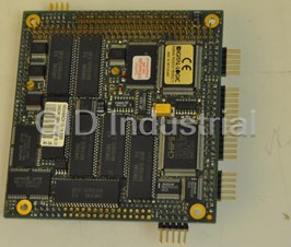


What they say about us
FANTASTIC RESOURCE
One of our top priorities is maintaining our business with precision, and we are constantly looking for affiliates that can help us achieve our goal. With the aid of GID Industrial, our obsolete product management has never been more efficient. They have been a great resource to our company, and have quickly become a go-to supplier on our list!
Bucher Emhart Glass
EXCELLENT SERVICE
With our strict fundamentals and high expectations, we were surprised when we came across GID Industrial and their competitive pricing. When we approached them with our issue, they were incredibly confident in being able to provide us with a seamless solution at the best price for us. GID Industrial quickly understood our needs and provided us with excellent service, as well as fully tested product to ensure what we received would be the right fit for our company.
Fuji
HARD TO FIND A BETTER PROVIDER
Our company provides services to aid in the manufacture of technological products, such as semiconductors and flat panel displays, and often searching for distributors of obsolete product we require can waste time and money. Finding GID Industrial proved to be a great asset to our company, with cost effective solutions and superior knowledge on all of their materials, it’d be hard to find a better provider of obsolete or hard to find products.
Applied Materials
CONSISTENTLY DELIVERS QUALITY SOLUTIONS
Over the years, the equipment used in our company becomes discontinued, but they’re still of great use to us and our customers. Once these products are no longer available through the manufacturer, finding a reliable, quick supplier is a necessity, and luckily for us, GID Industrial has provided the most trustworthy, quality solutions to our obsolete component needs.
Nidec Vamco
TERRIFIC RESOURCE
This company has been a terrific help to us (I work for Trican Well Service) in sourcing the Micron Ram Memory we needed for our Siemens computers. Great service! And great pricing! I know when the product is shipping and when it will arrive, all the way through the ordering process.
Trican Well Service
GO TO SOURCE
When I can't find an obsolete part, I first call GID and they'll come up with my parts every time. Great customer service and follow up as well. Scott emails me from time to time to touch base and see if we're having trouble finding something.....which is often with our 25 yr old equipment.
ConAgra Foods