

 Manufacturers
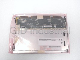
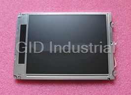
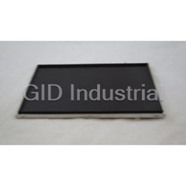
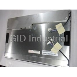
AU OPTRONICS T260XW02 V5
Description
AU OPTRONICS- T260XW02 V5-26" LCD Panel
Part Number
T260XW02 V5
Price
Request Quote
Manufacturer
AU OPTRONICS
Lead Time
Request Quote
Category
LCDS & PANEL DISPLAYS
Specifications
Active Screen Size
26.0 inches
BL Structure
8 U-Lamps
Display Area
575.769 (H) x 323.712(V) mm
Display Colors
16.7M Colors
Display Mode
Normally Black
Driver Element
a-Si TFT active matrix
Number of Pixels
1366 x 768 Pixel
Outline Dimension
626.0 (H) x 373.0 (V) x 47.5(D) mm With inverter
Pixel Arrangement
RGB vertical stripe
Pixel Pitch
0.4215 mm
Surface Treatment
AG, 3H
Datasheet

Extracted Text
Document Version: 5.1 Date: 2005/9/19 Product Specifications 26.0” WXGA Color TFT-LCD Module Model Name: T260XW02 (*) Preliminary Specifications ( ) Final Specifications ◎Copyright AU Optronics, Inc. January, 2003 All Rights Reserved T260XW02 V5-Spec. Ver5.1 1/26 Contents No ITEM COVER CONTENTS RECORD OF REVISIONS 1 GENERAL DESCRIPTION 2 ABSOLUTION MAXIMUM RATINGS 3 ELECTRICAL SPECIFICATIONS 3-1 ELECTRICAL CHARACTERISTICS INTERFACE CONNECTIONS 3-2 SIGNAL TIMING SPECIFICATIONS 3-3 SIGNAL TIMING WAVEFORMS 3-4 3-5 COLOR INPUT DATA REFERENCE 3-6 POWER SEQUENCE 4 OPTICAL SPECIFICATIONS 5 MECHANICAL CHARACTERISTICS 6 RELIABILITY 7 INTERNATIONAL STANDARDS 7-1 SAFETY 7-2 EMC PACKING 8 PRECAUTIONS 9 ◎Copyright AU Optronics, Inc. January, 2003 All Rights Reserved T260XW02 V5-Spec. Ver5.1 2/26 Record of Revision Version Date No Old Description New Description Remark 5.0 2005/8/2 Original Version 2. Absolute Maximum Ratings 2. Absolute Maximum Ratings Page 5 Symbol: VDD Symbol: VDDB Optical Specificationè Optical Specificationè 5.1 2005/9/19 Contrast Ratioè 600 : 1(min) Contrast Ratioè 800 : 1(min) Page 15 1000 : 1 (typ.) 1000 : 1 (typ.) Dark Luminanceè 0.8 (max) Dark Luminanceè 0.625 (max) ◎Copyright AU Optronics, Inc. Ja , 2003 All Rights Reser d T260XW02 V5-Spec. Ver5.1 3/26 1. General Description This specification applies to the 26.0 inch Color TFT-LCD Module T260XW02. This LCD module has a TFT active matrix type liquid crystal panel 1366x768 pixels, and diagonal size of 26.0 inch. This module supports 1366x768 XGA-WIDE mode (Non-interlace). Each pixel is divided into Red, Green and Blue sub-pixels or dots which are arranged in vertical stripes. Gray scale or the brightness of the sub-pixel color is determined with a 8-bit gray scale signal for each dot. The T260XW02 has been designed to apply the 8-bit 1 channel LVDS interface method. It is intended to support displays where high brightness, wide viewing angle, high color saturation, and high color depth are very important. * General Information Items Specification Unit Note 26.0 inches Active Screen Size 575.769 (H) x 323.712(V) Display Area mm 0.4215 mm Pixel Pitch 626.0 (H) x 373.0 (V) x 47.5(D) mm With inverter Outline Dimension a-Si TFT active matrix Driver Element 16.7M Colors Display Colors 1366 x 768 Pixel Number of Pixels RGB vertical stripe Pixel Arrangement Normally Black Display Mode BL Structure 8 U-Lamps AG, 3H Surface Treatment ◎Copyright AU Optronics, Inc. Ja , 2003 All Rights Reser d T260XW02 V5-Spec. Ver5.1 4/26 epr 2. Absolute Maximum Ratings The following are maximum values which, if exceeded, may cause faulty operation or damage to the unit. Item Symbol Min Max Unit Conditions VCC -0.3 (6.0) [Volt] Note 1 Logic/LCD Drive Voltage Vin -0.3 (3.6) [Volt] Note 1 Input Voltage of Signal VDDB -0.3 27.0 [Volt] Note 1 BLU Input Voltage BLON -0.3 7.0 [Volt] Note 1 BLU Brightness Control Voltage o TOP 0 +50 [ C] Note 2 Operating Temperature HOP 10 90 [%RH] Note 2 Operating Humidity o TST -20 +60 [ C] Note 2 Storage Temperature HST 10 90 [%RH] Note 2 Storage Humidity Note 1 : Duration = 50msec Note 2 : Maximum Wet-Bulb should be 39℃ and No condensation. ◎Copyright AU Optronics, Inc. Ja , 2003 All Rights Reser d T260XW02 V5-Spec. Ver5.1 5/26 3. Electrical Specification The T260XW02 requires two power inputs. One is employed to power the LCD electronics and to drive the TFT array and liquid crystal. The second input power for the BLU, is to power inverter.. 3-1 Electrical Characteristics Values Symbol Unit Notes Parameter Min. Typ. Max. LCD: Power Supply Input Voltage Vcc 4.5 5.0 5.5 V Power Supply Input Current Icc - 1.40 1.78 mA 1 Power Consumption Pc - 7.0 9.0 Watt 1 Inrush Current I - - 3.0 A 2 RUSH Backlight Power Consumption 84 85 Watt Life Time 50,000 60,000 Hours 3 Note : 1. Vcc=5.0V, Fv=60Hz, Fclk= 85.0 MHz , 25℃. 2. Vcc rising time = 470 ms , Vcc=5.0V 3. The performance of the Lamp in LCM, for example: lifetime or brightness, is extremely influenced by the characteristics of the DC-AC Inverter. So all the parameters of an inverter should be carefully designed so as not to produce too much leakage current from high-voltage output of the inverter. When you design or order the inverter, please make sure unwanted lighting caused by the mismatch of the lamp and the inverter (no lighting, flicker, etc) never occurs. When you confirm it, the LCD Assembly should be operated in the same condition as installed in your instrument. 4. Do not attach a conducting tape to lamp connecting wire. If the lamp wire attach to conducting tape, TFT-LCD Module have a low luminance and the inverter has abnormal action because leakage current occurs between lamp wire and conducting tape. 5. The relative humidity must not exceed 80% non-condensing at temperatures of 40℃ or less. At temperatures greater than 40℃, the wet bulb temperature must not exceed 39℃. When operate at low temperatures, the brightness of CCFL will drop and the lifetime of CCFL will be reduced. ◎Copyright AU Optronics, Inc. January, 2003 All Rights Reserved T260XW02 V5-Spec. Ver5.1 6/26 3-2 Interface Connections LCD connector (CN1): JAE FI-E30S or equivalent - - Mating Connector: - LVDS Transmitter: SN75LVDS83(Texas Instruments) or equivalent Note: 1. All GND (ground) pins should be connected together and should also be connected to the LCD ’s metal frame. All Vcc (power input) pins should be connected together. Pin No Symbol Description Default 1 N.C. No Connection (Reserved for aging mode internally) 2 N.C. No Connection (Reserved for I2C clock input) 3 N.C. No Connection (Reserved for I2C data input) 4 GND Power Ground 5 Rx0- Negative LVDS differential data input 6 Rx0+ Positive LVDS differential data input 7 GND Power Ground 8 Rx1- Negative LVDS differential data input 9 Rx1+ Positive LVDS differential data input 10 GND Power Ground 11 Rx2- Negative LVDS differential data input 12 Rx2+ Positive LVDS differential data input 13 GND Power Ground 14 RxCLK- Negative LVDS differential clock input 15 RxCLK+ Positive LVDS differential clock input 16 GND Power Ground 17 Rx3- Negative LVDS differential clock input (Even clock) 18 Rx3+ Positive LVDS differential clock input (Even clock) 19 GND Power Ground 20 Reserved No Connection ( Auo internal Test Pin) 21 LVDS Option Pull Low : JETDA LVDS format; Pull High or N.C.: NS LVDS format 22 N.C. Reserved 23 GND Power Ground 24 GND Power Ground 25 GND Power Ground 26 V +5V Power Input CC 27 V +5V Power Input CC 28 V +5V Power Input CC 29 V +5V Power Input CC 30 V +5V Power Input CC ** LVDS Option : H (3.3V) or N.C.è NS (Normal) L (GND) è JETDA ◎Copyright AU Optronics, Inc. Ja , 2003 All Rights Reser d T260XW02 V5-Spec. Ver5.1 7/26 epr LVDS Option = H (3.3V) Previous Cycle Current Cycle Next Cycle Clock RIN0+ R3 R2 G2 R7 R6 R5 R4 R3 R2 G2 RIN0- RIN1+ G4 G3 B3 B2 G6 G6 G5 G4 G3 B3 RIN1- RIN2+ B5 B4 DE NA NA B7 B6 B5 B4 DE RIN2- RIN3+ R1 R0 NA B1 B0 G1 G0 R1 R0 NA RIN3- LVDS Option = GND or OPEN Previous Cycle Current Cycle Next Cycle Clock RIN0+ R1 R0 G0 R5 R4 R3 R2 R1 R0 G0 RIN0- RIN1+ G2 G1 B1 B0 G5 G4 G3 G2 G1 B1 RIN1- RIN2+ B3 B2 DE NA NA B5 B4 B4 B2 DE RIN2- RIN3+ R7 R6 NA B7 B6 G7 G6 R7 R6 NA RIN3- ◎Copyright AU Optronics, Inc. Januar , 2003 All Rights Reser ed T260XW02 V5-Spec. Ver5.1 8/26 BACKLIGHT CONNECTOR PIN CONFIGURATION 1. Electrical specification (Ta=25±5℃) No ITEM SYMBOL CONDITION MIN TYP MAX UNIT Note 1 --- 21.6 24.0 26.4 V Input Voltage V DD V =24V DD 2 Input Current I --- --- 3.6 A DD Max. Brightness V =24V DD --- --- 85 W 3 Input Power P DD Dimming Max. V =24V DD 4 I --- --- 5 A Input inrush current, 0.3ms RUSH Dimming Max. V =24V --- 48 --- kHz 5 Output Frequency F BL DD ON V =24V 2.0 --- 3.3 V or Open DD 6 ON/OFF Control Voltage V BLON OFF V =24V 0.0 --- 0.8 V DD 7 ON/OFF Control Current I V =24V -1 --- 1.5 mA DD BLON MAX V =24V --- 3.3 --- V or Open DD 8 Dimming Control Voltage V DIM MIN V =24V --- 0.0 --- V DD MIN V =24V 1.0 --- mA 9 Dimming Control Current I DIM DD MAX --- 2.0 --- 3.3 V 10 External PWM Control Voltage EV PWM MIN --- -0.3 --- 0.8 V MAX PWM=100% 0.5 --- --- mA 11 External PWM Control Current EI PWM MIN PWM=100% 0.5 --- --- mA 12 --- 30 --- 100 % or Open External PWM Duty Ratio ED PWM 13 EF --- 150 --- 300 Hz External PWM Frequency PWM 2. Input specification Pin No Symbol Description Default 1 VDD Operating Voltage Supply, +24V DC regulated 24V 2 VDD Operating Voltage Supply, +24V DC regulated 24V 3 VDD Operating Voltage Supply, +24V DC regulated 24V 4 VDD Operating Voltage Supply, +24V DC regulated 24V 5 VDD Operating Voltage Supply, +24V DC regulated 24V 6 GND Ground GND 7 GND Ground GND 8 GND Ground GND 9 GND Ground GND 10 GND Ground GND 11 Analog DIM External Analog Dimming Control - 12 BL ON/OFF On/Off Control - 13 PWM DIM External PWM Dimming Control - 14 Reserved N.C. - CN1: S14B-PH-SM3-TB(JST) or Compatible CN2: S2B-ZR-SM3A-TF(JST) or Compatible CN3~10: SM02(12)B-BHS-1-TB(JST) or Compatible ◎Copyright AU Optronics, Inc. January, 2003 All Rights Reserved. T260XW02 V5-Spec. Ver5.1 9/26 3. Backlight Diagram HOT: High Voltage HOT 1(PINK) HOT 2(WHITE) HOT 3(PINK) HOT 4(WHITE) HOT 13(PINK) HOT 14(WHITE) HOT 15(PINK) HOT 16(WHITE) ◎Copyright AU Optronics, Inc. January, 2003 All Rights Reserved. T260XW02 V5-Spec. Ver5.1 10/26 3-3 Signal Timing Specifications This is the signal timing required at the input of the User connector. All of the interface signal timing should be satisfied with the following specifications for it ’s proper operation. * Timing Table DE only Mode Vertical Frequency Range A Signal Item Symbol Min. Typ. Max. Unit Period Tv 789 806 822 Th Vertical Tdisp 768 Th Active Section Tblk (v) 21 38 54 Th Blanking Period Th 1414 1560 1722 Tclk Horizontal Active Tdisp 1366 Tclk Section Tblk (h) 48 194 356 Tclk Blanking Clock Frequency Fclk 54 63 74 MHz Vertical Frequency Fv 48 50 52 Hz Frequency Horizontal Freq 39.45 --- 41.10 kHz Frequency Frequency Vertical Frequency Range B Signal Item Symbol Min. Typ. Max. Unit Tv 789 806 822 Th Period Vertical Tdisp 768 Th Active Section Tblk (v) 21 38 54 Th Blanking Period Th 1414 1560 1722 Tclk Horizontal Tdisp 1366 Tclk Active Section Tblk (h) 48 194 356 Tclk Blanking Clock Frequency Fclk 65 76 88 MHz Vertical Frequency Fv 58 60 62 Hz Frequency Horizontal Freq 47.32 --- 49.32 kHz Frequency Frequency *1) DCLK signal input must be valid while power supply is applied. *2) Display position is specific by the rise of ENAB signal only. st Horizontal display position is specified by the falling edge of 1 DCLK right after the rise of ENAB, is displayed on the left edge of the screen. Vertical display position is specified by the rise of ENAB after a “Low” level period equivalent to eight times st of horizontal period. The 1 data corresponding to one horizontal line after the rise of ENAB is displayed at the top line of screen. *3.) If a period of ENAB “High” is less than 1366 DCLK or less than 768 lines, the rest of the screen displays black. *4.) The display position does not fit to the screen if a period of ENAB “High” and the effective data period do not synchronize with each other. ◎Copyright AU Optronics, Inc. January, 2003 All Rights Reserved T260XW02 V5-Spec. Ver5.1 11/26 Tv Tblk(v) Tdisp(v) Th DE RGB 1366 Invalid Data 1 2 3 4 1366 Invalid Data Data Line Line Line Line Line Line CLK Th Tclk Tdisp(h) Tblk(h) DE Pixel Pixel Pixel Pixel Pixel Pixel Pixel Pixel Pixel Pixel Pixel RGB Data Invalid Data Invalid Data 768 1 2 3 4 5 6 767 768 1 3 3-4 Signal Timing Waveforms ◎Copyright AU Optronics, Inc. January, 2003 All Rights Reserved. T260XW02 V5-Spec. Ver5.1 12/26 3-5 Color Input Data Reference The brightness of each primary color (red, green and blue) is based on the 8 bit gray scale data input for the color; the higher the binary input, the brighter the color. The table below provides a reference for color versus data input. COLOR DATA REFERENCE Input Color Data RED GREEN BLUE Color MSB LSB MSB LSB MSB LSB R7 R6 R5 R4 R3 R2 R1 R0 G7 G6 G5 G4 G3 G2 G1 G0 B7 B6 B5 B4 B3 B2 B1 B0 Black 0 0 0 0 0 0 0 0 0 0 0 0 0 0 0 0 0 0 0 0 0 0 0 0 Red(255) 1 1 1 1 1 1 1 1 0 0 0 0 0 0 0 0 0 0 0 0 0 0 0 0 0 0 0 0 0 0 0 0 1 1 1 1 1 1 1 1 0 0 0 0 0 0 0 0 Green(255) Blue(255) 0 0 0 0 0 0 0 0 0 0 0 0 0 0 0 0 1 1 1 1 1 1 1 1 Basic Cyan 0 0 0 0 0 0 0 0 1 1 1 1 1 1 1 1 1 1 1 1 1 1 1 1 Color 1 1 1 1 1 1 1 1 0 0 0 0 0 0 0 0 1 1 1 1 1 1 1 1 Magenta Yellow 1 1 1 1 1 1 1 1 1 1 1 1 1 1 1 1 0 0 0 0 0 0 0 0 1 1 1 1 1 1 1 1 1 1 1 1 1 1 1 1 1 1 1 1 1 1 1 1 White RED(000) 0 0 0 0 0 0 0 0 0 0 0 0 0 0 0 0 0 0 0 0 0 0 0 0 RED(001) 0 0 0 0 0 0 0 0 0 0 0 0 0 0 0 0 0 0 0 0 0 0 0 0 RED ---- RED(254) 1 1 1 1 1 1 1 0 0 0 0 0 0 0 0 0 0 0 0 0 0 0 0 0 1 1 1 1 1 1 1 1 0 0 0 0 0 0 0 0 0 0 0 0 0 0 0 0 RED(255) GREEN(000) 0 0 0 0 0 0 0 0 0 0 0 0 0 0 0 0 0 0 0 0 0 0 0 0 GREEN(001) 0 0 0 0 0 0 0 0 0 0 0 0 0 0 0 1 0 0 0 0 0 0 0 0 GREEN ---- GREEN(254) 0 0 0 0 0 0 0 0 1 1 1 1 1 1 1 0 0 0 0 0 0 0 0 0 0 0 0 0 0 0 0 0 1 1 1 1 1 1 1 1 0 0 0 0 0 0 0 0 GREEN(255) BLUE(000) 0 0 0 0 0 0 0 0 0 0 0 0 0 0 0 0 0 0 0 0 0 0 0 0 BLUE(001) 0 0 0 0 0 0 0 0 0 0 0 0 0 0 0 0 0 0 0 0 0 0 0 1 ------- BLUE BLUE(254) 0 0 0 0 0 0 0 0 0 0 0 0 0 0 0 0 1 1 1 1 1 1 1 0 BLUE(255) 0 0 0 0 0 0 0 0 0 0 0 0 0 0 0 0 1 1 1 1 1 1 1 1 ◎Copyright AU Optronics, Inc. January, 2003 All Rights Reserved. T260XW02 V5-Spec. Ver5.1 13/26 3-6 Power Sequence 90% 90% Power Supply For LCD 10% 10% 10% VCC (+5V) & VDD GND t1 t2 t5 t6 t7 Interface Signal Valid Data 10% 10% GND t3 t4 Power For LAMP (BLON) Values Parameter Units Min. Typ. Max. t1 470 - 1000 μs t2 25 - 60 ms 600 - - ms t3 t4 200 - - ms 50 - - ms t5 t6 0.47 - 30 ms t7 1 - - s ◎Copyright AU Optronics, Inc. January, 2003 All Rights Reserved. T260XW02 V5-Spec. Ver5.1 14/26 4. Optical Specification Optical characteristics are determined after the unit has been ‘ON’ and stable for approximately 45 minutes in a dark environment at 25℃. The values specified are at an approximate distance 50cm from the LCD surface at a viewing angle of Φ and θequal to 0°. Fig.1 1 presents additional information concerning the measurement equipment and method. Values Parameter Symbol Units Notes Min. Typ. Max. Contrast Ratio 1 CR (800) (1000) Dark Luminance LBK (0.625) cd/㎡ 2 Surface Luminance, white LWH 400 500 cd/㎡ Luminance Variation 3 δ 9 p 1.4 WHITE Response Rise Time Tr 15 18 R ms 4 Time Tr 5 7 Decay Time D Gray to Gray 5 Tγ 8 35 ms Color Coordinates R 0.640 X RED R 0.330 Y G 0.290 X GREEN G 0.600 Y Typ.-0.03 Typ.+0.03 B 0.150 X BLUE B 0.060 Y W 0.280 X WHITE W 0.290 Y Viewing Angle x axis, right(φ=0°) θ 85 Degree r x axis, left(φ=180°) θ 85 Degree 6 l y axis, up(φ=90°) θ 85 Degree u y axis, down (φ=0°) θ 85 Degree d ◎Copyright AU Optronics, Inc. January, 2003 All Rights Reserved. T260XW02 V5-Spec. Ver5.1 15/26 Note: 1. Contrast Ratio (CR) is defined mathematically as: Surface Luminance of L on1 Contrast Ratio= Surface Luminance of L off1 2. Surface luminance is luminance value at point 1 across the LCD surface 50cm from the surface with all pixels displaying white. From more information see FIG 2. When V = 24V, I = 3.5A. L =Lon1 DDB DDB WH Where Lon1 is the luminance with all pixels displaying white at center 1 location. 3. The variation in surface luminance, δ is defined (center of Screen) as: WHITE δ = Maximum(L , L ,…L ) / Minimum(L , L ,…,L ) WHITE(9P) on1 on2 on9 on1 on2 on9 4. Response time is the time required for the display to transition from black to white(Rise Time, Tr ) and from white to black R (Decay Time, Tr ). For additional information see FIG3. D 5. Tγ is the response time between any two gray scale and is based on f =60Hz to optimize. v 6. Viewing angle is the angle at which the contrast ratio is greater than 10. The angles are determined for the horizontal or x axis and the vertical or y axis with respect to the z axis which is normal to the LCD surface. For more information see FIG4. V FIG. 2 Luminance 2 3 1 H/2 4 5 6 H 7 8 H/6 V/6 V/2 ◎Copyright AU Optronics, Inc. January, 2003 All Rights Reserved T260XW02 V5-Spec. Ver5.1 16/26 FIG.3 Response Time The response time is defined as the following figure and shall be measured by switching the input signal for “black” and “white”. Any brighter gray level (White) Any brighter gray level (White) 100% 90% Optical Response n a n c e Any darker gray (Black) 10% 0 Tr Tr Time D R FIG.4 Viewing angle ◎Copyright AU Optronics, Inc. January, 2003 All Rights Reserved. T260XW02 V5-Spec. Ver5.1 17/26 5. Mechanical Characteristics The contents provide general mechanical characteristics for the model T260XW02. In addition the figures in the next page are detailed mechanical drawing of the LCD. Horizontal 626.0mm Vertical 373.0mm Outline Dimension 47.5mm(w/i inverter & Shielding) Depth 30.3mm(w/o inverter) Horizontal 580.8mm Bezel Area Vertical 328.8mm Horizontal 575.769mm Active Display Area Vertical 323.712mm Weight 4200g (Typ.) Surface Treatment Anti-Glare, 3H ◎Copyright AU Optronics, Inc. January, 2003 All Rights Reserved. T260XW02 V5-Spec. Ver5.1 18/26 Front View ◎Copyright AU Optronics, Inc. January, 2003 All Rights Reserved T260XW02 V5-Spec. Ver5.1 19/26 notes: 1. l A-B l<1.6mm 2. l C-D l<1.6mm Rear View ◎Copyright AU Optronics, Inc. January, 2003 All Rights Reserved T260XW02 V5-Spec. Ver5.1 20/26 6. Reliability Environment test condition No Test Item Condition 1 High temperature storage test Ta=60℃ 240h 2 Low temperature storage test Ta=-20℃ 240h 3 High temperature operation test Ta=50℃ 80%RH 240h 4 Low temperature operation test Ta=0℃ 240h Wave form: random Vibration level: 1.0G RMS Vibration test Bandwidth: 10-500Hz 5 (non-operating) Duration: X, Y, Z 20min One time each direction Shock level: 100G Waveform: half since wave, 2ms Shock test 6 Direction: ±X, ±Y, ±Z (non-operating) One time each direction Vibration test Random Vibration: 10~200Hz, 1.5G, 30minutes 7 (with carton) in each X, Y, Z direction Height: 53.3cm Drop test 1 corner, 3 edges, 6 surfaces 8 (with carton) (ASTMD4169-I) Altitude 9 50,000 feet (12Kpa) Storage/shipment {Result Evaluation Criteria} There should be no change which might affect the practical display function when the display quality test is conducted under normal operating condition. ◎Copyright AU Optronics, Inc. January, 2003 All Rights Reserved T260XW02 V5-Spec. Ver5.1 21/26 7. International Standard 7-1. Safety (1) UL1950 Third Edition, Underwriters Laboratories, Inc. Jan. 28, 1995 Standard for Safety of Information Technology Equipment Including electrical Business Equipment. (2) CAN/CSA C22.2 No. 950-95 Third Edition, Canadian Standards Association, Jan. 28, 1995 Standard for Safety of Information Technology Equipment Including Electrical Business Equipment. (3) EN60950 : 1992+A2: 1993+A2: 1993+C3: 1995+A4: 1997+A11: 1997 IEC 950: 1991+A1: 1992+A2: 1993+C3: 1995+A4:1996 European Committee for Electrotechnical Standardization (CENELEC) EUROPEAN STANDARD for Safety of Information Technology Equipment Including Electrical Business Equipment. 7-2. EMC a) ANSI C63.4 “Methods of Measurement of Radio-Noise Emissions from Low-Voltage Electrical and Electrical Equipment in the Range of 9kHz to 40GHz. “American National standards Institute(ANSI), 1992. b) C.I.S.P.R “Limits and Methods of Measurement of Radio Interface Characteristics of Information Technology Equipment.” International Special committee on Radio Interference. c) EN 55022 “Limits and Methods of Measurement of Radio Interface Characteristics of Information Technology Equipment.” European Committee for Electrotechnical Standardization. (CENELEC), 1998. ◎Copyright AU Optronics, Inc. January, 2003 All Rights Reserved T260XW02 V5-Spec. Ver5.1 22/26 8. Packing Label sample 83mm * 23mm Carton Label AU Optronics QTY: 4 MODEL NO: T260XW02 VX PART NO: 97.26T02.XXX CUSTOMER NO: CARTON NO: Made in Taiwan *PM100-01A1600001* ◎Copyright AU Optronics, Inc. January, 2003 All Rights Reserved T260XW02 V5-Spec. Ver5.1 23/26 Carton Size 767(L)mm*330(W)mm*480(H)mm 4pcs Modules Cushion top Cushion set Cushion down V 4pcs / 1 carton ◎Copyright AU Optronics, Inc. January, 2003 All Rights Reserved T260XW02 V5-Spec. Ver5.1 24/26 9. PRECAUTIONS Please pay attention to the followings when you use this TFT LCD module. 9-1 MOUNTING PRECAUTIONS (1) You must mount a module using holes arranged in four corners or four sides. (2) You should consider the mounting structure so that uneven force (ex. Twisted stress) is not applied to module. And the case on which a module is mounted should have sufficient strength so that external force is not transmitted directly to the module. (3) Please attach the surface transparent protective plate to the surface in order to protect the polarizer. Transparent protective plate should have sufficient strength in order to the resist external force. (4) You should adopt radiation structure to satisfy the temperature specification. (5) Acetic acid type and chlorine type materials for the cover case are not desirable because the former generates corrosive gas of attacking the polarizer at high temperature and the latter causes circuit break by electro-chemical reaction. (6) Do not touch, push or rub the exposed polarizers with glass, tweezers or anything harder than HB pencil lead. And please do not rub with dust clothes with chemical treatment. Do not touch the surface of polarizer for bare hand or greasy cloth. (Some cosmetics are detrimental to the polarizer.) (7) When the surface becomes dusty, please wipe gently with absorbent cotton or other soft materials like chamois soaks with petroleum benzene. Normal-hexane is recommended for cleaning the adhesives used to attach front/ rear polarizers. Do not use acetone, toluene and alcohol because they cause chemical damage to the polarizer. (8) Wipe off saliva or water drops as soon as possible. Their long time contact with polarizer causes deformations and color fading. (9) Do not open the case because inside circuits do not have sufficient strength. 9-2 OPERATING PRECAUTIONS (1) The spike noise causes the mis-operation of circuits. It should be lower than following voltage: V= ±200mV(Over and under shoot voltage) (2) Response time depends on the temperature. (In lower temperature, it becomes longer..) (3) Brightness depends on the temperature. (In lower temperature, it becomes lower.) And in lower temperature, response time (required time that brightness is stable after turned on) becomes longer. (4) Be careful for condensation at sudden temperature change. Condensation makes damage to polarizer or electrical contacted parts. And after fading condensation, smear or spot will occur. (5) When fixed patterns are displayed for a long time, remnant image is likely to occur. (6) Module has high frequency circuits. Sufficient suppression to the electromagnetic interference shall be done by system manufacturers. Grounding and shielding methods may be important to minimize the interface. ◎Copyright AU Optronics, Inc. January, 2003 All Rights Reserved T260XW02 V5-Spec. Ver5.1 25/26 9-3 ELECTROSTATIC DISCHARGE CONTROL Since a module is composed of electronic circuits, it is not strong to electrostatic discharge. Make certain that treatment persons are connected to ground through wrist band etc. And don’t touch interface pin directly. 9-4 PRECAUTIONS FOR STRONG LIGHT EXPOSURE Strong light exposure causes degradation of polarizer and color filter. 9-5 STORAGE When storing modules as spares for a long time, the following precautions are necessary. (1) Store them in a dark place. Do not expose the module to sunlight or fluorescent light. Keep the temperature between 5℃ and 35℃ at normal humidity. (2) The polarizer surface should not come in contact with any other object. It is recommended that they be stored in the container in which they were shipped. 9-6 HANDLING PRECAUTIONS FOR PROTECTION FILM (1) The protection film is attached to the bezel with a small masking tape. When the protection film is peeled off, static electricity is generated between the film and polarizer. This should be peeled off slowly and carefully by people who are electrically grounded and with well ion-blown equipment or in such a condition, etc. (2) When the module with protection film attached is stored for a long time, sometimes there remains a very small amount of flue still on the Bezel after the protection film is peeled off. (3) You can remove the glue easily. When the glue remains on the Bezel or its vestige is recognized, please wipe them off with absorbent cotton waste or other soft material like chamois soaked with normal-hexane. ◎Copyright AU Optronics, Inc. January, 2003 All Rights Reserved T260XW02 V5-Spec. Ver5.1 26/26
Frequently asked questions
What makes Elite.Parts unique?

What kind of warranty will the T260XW02 V5 have?
Which carriers does Elite.Parts work with?
Will Elite.Parts sell to me even though I live outside the USA?
I have a preferred payment method. Will Elite.Parts accept it?
Why buy from GID?

Quality
We are industry veterans who take pride in our work

Protection
Avoid the dangers of risky trading in the gray market

Access
Our network of suppliers is ready and at your disposal

Savings
Maintain legacy systems to prevent costly downtime

Speed
Time is of the essence, and we are respectful of yours
Related Products
Au Optronics G084SN05 8.4" TFT 800 x 600 SVGA LCD Module
Au Optronics M150XN04 15" TFT 1024 x 768 XGA LCD Module
AU Optronics M150XN07 V2 LCD Panel - 15" LCD Panel
AU optronics M201EW01-V3 20.1" LCD Panel
AU Optronics T315XW01 V5 31.5" LCD Panel
AU Optronics T370XW01 V1 37" LCD Panel
Request a Quote

The quote request has been received
Close

Facing challenges or have inquiries? Feel free to contact us!
Call Us +1-469-283-2440
What they say about us
FANTASTIC RESOURCE
One of our top priorities is maintaining our business with precision, and we are constantly looking for affiliates that can help us achieve our goal. With the aid of GID Industrial, our obsolete product management has never been more efficient. They have been a great resource to our company, and have quickly become a go-to supplier on our list!
Bucher Emhart Glass
EXCELLENT SERVICE
With our strict fundamentals and high expectations, we were surprised when we came across GID Industrial and their competitive pricing. When we approached them with our issue, they were incredibly confident in being able to provide us with a seamless solution at the best price for us. GID Industrial quickly understood our needs and provided us with excellent service, as well as fully tested product to ensure what we received would be the right fit for our company.
Fuji
HARD TO FIND A BETTER PROVIDER
Our company provides services to aid in the manufacture of technological products, such as semiconductors and flat panel displays, and often searching for distributors of obsolete product we require can waste time and money. Finding GID Industrial proved to be a great asset to our company, with cost effective solutions and superior knowledge on all of their materials, it’d be hard to find a better provider of obsolete or hard to find products.
Applied Materials
CONSISTENTLY DELIVERS QUALITY SOLUTIONS
Over the years, the equipment used in our company becomes discontinued, but they’re still of great use to us and our customers. Once these products are no longer available through the manufacturer, finding a reliable, quick supplier is a necessity, and luckily for us, GID Industrial has provided the most trustworthy, quality solutions to our obsolete component needs.
Nidec Vamco
TERRIFIC RESOURCE
This company has been a terrific help to us (I work for Trican Well Service) in sourcing the Micron Ram Memory we needed for our Siemens computers. Great service! And great pricing! I know when the product is shipping and when it will arrive, all the way through the ordering process.
Trican Well Service
GO TO SOURCE
When I can't find an obsolete part, I first call GID and they'll come up with my parts every time. Great customer service and follow up as well. Scott emails me from time to time to touch base and see if we're having trouble finding something.....which is often with our 25 yr old equipment.
ConAgra Foods