

 Manufacturers
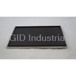
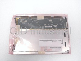
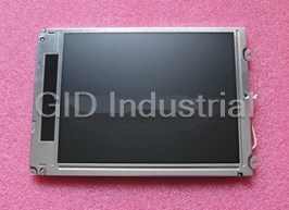
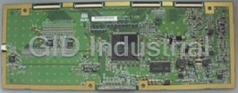
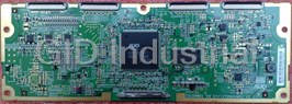
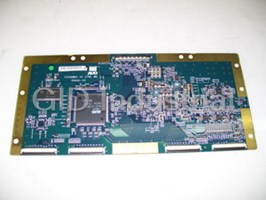
AU OPTRONICS M150XN07 V2
Description
AU Optronics M150XN07 V2 LCD Panel - 15" LCD Panel
Part Number
M150XN07 V2
Price
Request Quote
Manufacturer
AU OPTRONICS
Lead Time
Request Quote
Category
LCDS & PANEL DISPLAYS
Specifications
Brightness uniformity
80% typ. (note 2)
Contrast Ratio
400 : 1 typ.
Crosstalk(at 60Hz)
1.2% max. (note 4)
DisplayArea
304.128 (H) x 228.096(38.1cmd
DisplayMode
TN mode, Normally White
Electrical Interface
LVDS(1 ch)
Frame rate
60Hztyp., 75Hz max.
Luminance uniformity
1.7 max.(Note 3)
Mounting method
Side mounting
Outline dimension
326.5 x 253.5 x 12.0 typ.
Pixel Arrangement
R.G.B. VerticalStripe
Pixel Pitch
0.297 x 0.297
Resolution
1024(R,G,B x 3) x 768
Screen diagonal
381 (15”)
Support Colors
262,144 colors (6-bit forR,G,B)
Surface treatment
Anti-glare, hard coating (3H)
Typical white Luminan
250nit (typ) @8mA (note 1)
Weight
1100 typ.
Features
- 2 CCFLs (Cold cathode Fluorescent Lamp)
- High contrast ratio, high aperture ratio
- High-speed response
- Lowpower consumption
- Wide viewing angle
- XGA 1024(H) x768(V) resolution
Datasheet

Extracted Text
Spec. No.: DDPM-M150XN07-0.1 Version: 1 Total pages: 26 Date: 2003-July-31 AU OPTRONICS CORPORATION Product Specifications 15.0 ” XGA Color TFT-LCD Module Model Name: M150XN07 V.1 Approved by Prepared by DDBU Marketing Division / AU Optronics Croporation Customer Checked & Approved by (C) Copyright AU Optronics, Inc. Feb. 2003 All Rights Reserved. M150XN07 Ver0.1 1/28 No Reproduction and Redistribution Allowed. Product Specifications 15.0 ” XGA Color TFT-LCD Module Model Name:M150XN07 V.1 (u) Preliminary Specifications ( ) Final Specifications (C) Copyright AU Optronics, Inc. Feb. 2003 All Rights Reserved. M150XN07 Ver0.1 2/28 No Reproduction and Redistribution Allowed. i Contents 1.0 Handling Precautions 2.0 General Description 2.1 Display Characteristics 2.2 Functional Block Diagram 3.0 Absolute Maximum Ratings 4.0 Optical Characteristics 4.1 Signal for Lamp connector 4.2 Parameter guideline for CCFL Inverter 5.0 Signal Interface 5.1 Module Interface Connectors 5.2 Module Connector Pin Configuration 5.3 Backlight Connectors 5.4 Backlight Connector Pin Configuration 5.5 Signal Electrical Characteristics 5.6 Interface Timings Characteristics 5.7 Interface Timing Definition 6.0 Pixel format image 7.0 Power Consumption 8.0 Power ON/OFF Sequence 9.0 Backlight Characteristics 9.1 Signal for Lamp connector 9.2 Parameter guideline for CCFL Inverter 10.0Vibration, Shock, and Drop 10.1 Vibration & Shock 10.1.1 Vibration Test Spec 10.1.2 Shock Test Spec 10.2 Drop 11.0 Environment 11.1 Temperature and Humidity 11.1.1 Operating Conditions 11.1.2 Shipping Conditions 11.2 Atmospheric Pressure 11.3 Thermal Shock 12.0 Reliability 12.1 Failure criteria 12.2 Failure rate 12.2.1 Usage 12.2.2 Components de-rating 12.3 CCFL life 12.4 ON/OFF cycle (C) Copyright AU Optronics, Inc. Feb. 2003 All Rights Reserved. M150XN07 Ver0.1 3/28 No Reproduction and Redistribution Allowed. 13.0 Safety 13.1 Sharp edge requirement 13.2 Material 13.2.1 Toxicity 13.2.2 Flammability 13.3 Capacitors 13.4 Hazardous voltage 14.0 Other requirements 14.1 Smoke free design 14.2 National test lab requirement 15.0 Label 16.0 Mechanical Characteristics ii Record of Revision Version and Date Page Old description New Description Remark 0.1 2003/06/10 All First Edition for Customer All (C) Copyright AU Optronics, Inc. Feb. 2003 All Rights Reserved. M150XN07 Ver0.1 4/28 No Reproduction and Redistribution Allowed. 1.0 Handling Precautions 1) Since front polarizer is easily damaged, pay attention not to scratch it. 2) Be sure to turn off power supply when inserting or disconnecting from input connector. 3) Wipe off water drop immediately. Long contact with water may cause discoloration or spots. 4) When the panel surface is soiled, wipe it with absorbent cotton or other soft cloth. 5) Since the panel is made of glass, it may break or crack if dropped or bumped on hard surface. 6) Since CMOS LSI is used in this module, take care of static electricity and insure human earth when handling. 7) Do not open nor modify the Module Assembly. 8) Do not press the reflector sheet at the back of the module to any directions. 9) In case if a Module has to be put back into the packing container slot after once it was taken out from the container, do not press the center of the CCFL Reflector edge. Instead, press at the far ends of the CFL Reflector edge softly. Otherwise the TFT Module may be damaged. 10) At the insertion or removal of the Signal Interface Connector, be sure not to rotate nor tilt the Interface Connector of the TFT Module. 11) After installation of the TFT Module into an enclosure (LCD monitor housing, for example), do not twist nor bend the TFT Module even momentary. At designing the enclosure, it should be taken into consideration that no bending/twisting forces are applied to the TFT Module from outside. Otherwise the TFT Module may be damaged. 12) Cold cathode fluorescent lamp in LCD contains a small amount of mercury. Please follow local ordinances or regulations for disposal. 13) Small amount of materials having no flammability grade is used in the LCD module. The LCD module should be supplied by power complied with requirements of Limited Power Source (2.11, IEC60950 or UL1950), or be applied exemption. 14) The LCD module is designed so that the CFL in it is supplied by Limited Current Circuit (2.4, IEC60950 or UL1950). Do not connect the CFL in Hazardous Voltage Circuit. (C) Copyright AU Optronics, Inc. Feb. 2003 All Rights Reserved. M150XN07 Ver0.1 5/28 No Reproduction and Redistribution Allowed. 2.0 General Description This specification applies to the 15.0 inch Color TFT-LCD Module M150XN07. The display supports the XGA (1024(H) x 768(V)) screen format and 262,144 colors (RGB 6-bits data). All input signals are 1 Channel LVDS interface compatible. This module does not contain an inverter card for backlight. Features -XGA 1024(H) x 768(V) resolution -2 CCFLs (Cold cathode Fluorescent Lamp) -High contrast ratio, high aperture ratio -Wide viewing angle -High-speed response -Low power consumption Application Desktop monitors 2.1 Display Characteristics The following items are characteristics summary on the table under 25 ℃ condition: ITEMS Unit SPECIFICATIONS Screen diagonal [mm] 381 (15”) Outline dimension [mm] 326.5 x 253.5 x 12.0 typ. Display Area [mm] 304.128 (H) x 228.096(38.1cm diagonal) Resolution 1024(R,G,B x 3) x 768 Pixel Pitch [mm] 0.297 x 0.297 Pixel Arrangement R.G.B. Vertical Stripe Display Mode TN mode, Normally White 2 Typical white Luminance. [cd/m ] 250nit (typ) @8mA (note 1) Brightness uniformity 80% typ. (note 2) Luminance uniformity 1.7 max.(Note 3) Crosstalk (at 60Hz) 1.2% max. (note 4) Contrast Ratio 400 : 1 typ. Support Colors 262,144 colors (6-bit for R,G,B) Chromaticity(CIE1931) White-x 0.313 White-y 0.329 Color Gamut 60% typ., of NTSC coverage Viewing angle 60(left),60(right),40(up),60(down) CR=10 Response Time [msec] 16ms typ. (Tr +Tf) Nominal Input Voltage VDD [Volt] +3.3 V Power Consumption [Watt] 15 (typ.) @8mA (All Black Pattern) (VDD line + CCFL line) Electrical Interface LVDS (1 ch) Frame rate [Hz] 60Hz typ., 75Hz max. Weight [Grams] 1100 typ. Mounting method Side mounting Surface treatment Anti-glare, hard coating (3H) Temperature Range o Operating [ C] 0 to +50 o Storage (Shipping) [ C] -20 to +60 (C) Copyright AU Optronics, Inc. Feb. 2003 All Rights Reserved. M150XN07 Ver0.1 6/28 No Reproduction and Redistribution Allowed. 256 512 768 3 2 192 1 384 5 4 576 Unit: pixels Note 1: Brightness is measured at the center point of brightness value with all pixels displaying white. 90 % 50 % 10 % 10 % 50 % 90 % Unit: percentage of dimension of display area Note 2: Brightness uniformity of these 9 points is defined as below: (Min. brightness / Max. brightness) x 100% Note 3: TCO ’99 Certification Requirements and test methods for environmental labeling of Display Report No. 2 defines Luminance uniformity as below: ((Lmax,+30deg. / Lmin,+30deg.) + (Lmax,-30deg. / Lmin,-30deg.)) / 2 (C) Copyright AU Optronics, Inc. Feb. 2003 All Rights Reserved. M150XN07 Ver0.1 7/28 No Reproduction and Redistribution Allowed. TCO 99 certification requirements and test methods: : 1) Diagrammatic m d L , °and L , ° max +30 min +30 Effective area:W ×H 2) D is the diagonal of the screen in centimeters. And m is as follow. d m (cm)=D×1.5 with a minimum distance:m =50 cm d d 3) The measurement positions shall consist of an active white square of size 4 by 4 cm. 4) Measure L , °and L , °that are given as points L & R. And then rotated to an azimuth angle of –30 max +30 min +30 degrees and measure L , °and L , °again using the same procedure. max -30 min -30 5) The variation in luminance ratio is calculated as the ratio: L =(( L , °/ L , °)+(L , °/ L , °))/2 ≦ 1.7 R max +30 min +30 max -30 min -30 Note 4: 1/2 1/6 2/3 1/2 1/3 1/6 1/6 A A’ 1/6 1/3 1/2 1/2 B B’ 2/3 184 gray level 184 gray level 0 gray level Unit: percentage of dimension of display area l L -L l / L x 100%= 1.2% max., L and L are brightness at location A and B A A’ A A B l L -L l / L x 100%= 1.2% max., L and L are brightness at location A’ and B’ B B’ B A’ B’ (C) Copyright AU Optronics, Inc. Feb. 2003 All Rights Reserved. M150XN07 Ver0.1 8/28 No Reproduction and Redistribution Allowed. Y-Driver IC Connector 2.2 Functional Block Diagram The following diagram shows the functional block of 15.0 inches Color TFT-LCD Module: AU ASIC G1 Timing TFT-LCD LVDS 1024*(3)*768 LVDS Pixels Receiver RSDS + 3.3 V G768 D1 D3072 2 CCFL DC/DC Gamma Converter Correction DC POWER Inverter DF-14H-20P-1.25H (Hirose) JST BHR-03VS-1 CWY20G-A0D1T (PTWO) (C) Copyright AU Optronics, Inc. Feb. 2003 All Rights Reserved. M150XN07 Ver0.1 9/28 No Reproduction and Redistribution Allowed. 3.0 Absolute Maximum Ratings Absolute maximum ratings of the module is as following: Item Symbol Min Max Unit Conditions Logic/LCD Drive Voltage VDD 0.3 +3.6 [Volt] Input Voltage of Signal Vin 0.3 VDD+0.3 [Volt] CCFL Current ICFL 3.0 8.5 [mA] rms Note 1 o Operating Temperature TOP 0 +50 [ C] Note 2 Operating Humidity HOP 20 85 [%RH] Note 2 o Storage Temperature TST -20 +60 [ C] Note 2 Storage Humidity HST 5 95 [%RH] Note 2 Vibration 1.5 / 10-200 [G / Hz] Shock 50/20 [G / ms] Half sine wave Assured Torque at Side Mount 2.0 [kgf.cm] Re-screw 3 [Times] Note 1: CCFL life time will drop dramatically if exceeding 8.0 mA; It will have safety concern if exceeding 8.5 mA. Note 2: Maximum Wet-Bulb should be 39℃ and No condensation. Wet bulb temperature chart Relative Humidity % Twb=39℃ T=40℃,H=95% 100 95 90 80 70 T=50 ,H=55% ℃ 60 T=60℃,H=39% 50 Storage range Operation range 40 T=65℃,H=29% 30 20 Storage range 10 5 0 -20 0 50 60 o Temperature C (C) Copyright AU Optronics, Inc. Feb. 2003 All Rights Reserved. M150XN07 Ver0.1 10/28 No Reproduction and Redistribution Allowed. 4.0 Optical Characteristics The optical characteristics are measured under stable conditions at 25 ℃ (Room Temperature): Item Unit Conditions Min. Typ. Max. Horizontal (Right) 50 60 [degree] CR = 10 (Left) 50 60 Viewing Angle [degree] Horizontal (Right) 60 75 CR =5 (Left) 60 75 Vertical (Upper) 30 40 [degree] CR = 10 (Lower) 50 60 CR: Contrast Ratio [degree] Vertical (Upper) 60 70 CR = 5 (Lower) 65 75 Contrast ratio Normal Direction 300 400 - Raising Time Ton Response Time( Note 1) [msec] - 4 6 ( 10%-90% ) Falling Time Toff [msec] - 12 17 ( 90%-10% ) [msec] Raising + Falling - 16 23 Color / Chromaticity Red x 0.587 0.617 0.647 Coordinates (CIE) Red y 0.317 0.347 0.377 Green x 0.260 0.290 0.320 Green y 0.563 0.593 0.623 Blue x 0.118 0.148 0.178 Blue y 0.070 0.100 0.130 White x Color Coordinates (CIE) White 0.283 0.313 0.343 White y 0.299 0.329 0.359 Brightness Uniformity [%] 75 80 - White Luminance at CCFL 8.0mA 200 250 - 2 [cd/m ] White Luminance at CCFL 6.5mA 170 200 - Crosstalk ( in 60Hz) [%] 1.2 Note 1: Definition of Response time: The output signals of photodetector are measured when the input signals are changed from “ Black” to “ White” (falling time), and from “White” to “ Black” (rising time), respectively. The response time interval between the 10% and 90% of amplitudes. Refer to figure as below. TrR TrD % 100 90 Optical Response 10 white white 0 black (C) Copyright AU Optronics, Inc. Feb. 2003 All Rights Reserved. M150XN07 Ver0.1 11/28 No Reproduction and Redistribution Allowed. 5.0 Signal Interface 5.1 Module Interface Connectors Physical interface is described as for the connector on module. These connectors are capable of accommodating the following signals and will be following components Interface Connector Connector Name Hirose, PTWO or compatible Manufacturer Type / Part Number DF-14H-20P-1.25H (Hirose) CWY20G-A0D1T (PTWO) 5.2 Module Connector Pin Configuration DF-14H-20P-1.25H (Hirose) or CWY20G-A0D1T (PTWO) Pin No. Symbol Description 1 VDD Power Supply, 3.3V (typical) 2 VDD Power Supply, 3.3V (typical) 3 VSS Ground 4 VSS Ground 5 Rin0- - LVDS differential data input (R0-R5, G0) 6 Rin0+ + LVDS differential data input (R0-R5, G0) 7 VSS Ground 8 Rin1- - LVDS differential data input (G1-G5, B0-B1) 9 Rin1+ + LVDS differential data input (G1-G5, B0-B1) 10 VSS Ground 11 Rin2- - LVDS differential data input (B2-B5, HS, VS, DE) 12 Rin2+ + LVDS differential data input (B2-B5, HS, VS, DE) 13 VSS Ground 14 ClkIN- - LVDS differential clock input 15 ClkIN+ + LVDS differential clock input 16 VSS Ground 17 Rin3- NC 18 Rin3+ NC 19 VSS Ground 20 NC Please *floating* and don’t connect to ground. (C) Copyright AU Optronics, Inc. Feb. 2003 All Rights Reserved. M150XN07 Ver0.1 12/28 No Reproduction and Redistribution Allowed. 5.3 Backlight Connectors For Lamp Connector Connector Name / Designation JST or compatible Manufacturer Type / Part Number BHR-03VS-1 SM02(8.0)B-BHS-1-TB Mating Type / Part Number 5.4 Backlight Connector Pin Configuration Pin Symbol Description 1 HV Lamp High Voltage 2 NC No connection 3 LV Ground u Cable length: 140 +- 5 mm u Connector-output position: right side (front view) u Lamp assy design shall be easy for replacement and repair. 5.5 Signal Electrical Characteristics Each signal characteristics are as follows; Item Symbol Min Typ Max Unit LCD Drive VDD +3.0 +3.3 +3.6 [V] voltage “High” input signal V ih 2.0 - - [V] voltage “Low” input signal V il - - 0.8 [V] voltage (C) Copyright AU Optronics, Inc. Feb. 2003 All Rights Reserved. M150XN07 Ver0.1 13/28 No Reproduction and Redistribution Allowed. 6bits input data format Clkln Vdiff=0V R0IN0 G0 R5 R4 R3 R2 R1 R0 R1IN1 B1 B0 G5 G4 G3 G2 G1 R2IN2 Note: R/G/B data 7:MSB, R/G/B data 0:LSB DE VS HS B5 B4 B3 B2 Previous Data for current Clk cycle Next (C) Copyright AU Optronics, Inc. Feb. 2003 All Rights Reserved. M150XN07 Ver0.1 14/28 No Reproduction and Redistribution Allowed. 5.6 Signal Electrical Characteristics Input signals shall be low or Hi-Z state when Vin is off It is recommended to refer to the specifications of SN75LVDS82DGG (Texas Instruments) in detail. Each signal characteristics are as follows: Parameter Condition Min Max Unit Differential InputHigh [mV] Vth 100 Voltage(Vcm=+1.2V) Differential Input Low [mV] Vtl -100 Voltage(Vcm=+1.2V) 5.7 Interface Timings Basically, interface timings described here is not actual input timing of LCD module but output timing of SN75LVDS82DGG (Texas Instruments) or equivalent. 5.7.1 Timing Characteristics Signal Parameter Symbol MIN TYP MAX Unit Clock Timing Clock frequency clk 50 65 81 MHz Hsync Timing Horizontal active Thd 1024 1024 1024 Tclk Horizontal blanking Thbl 40 320 400 Tclk Horizontal period Th 1064 1344 1424 Tck Vsync Timing Vertical active Tvd 768 768 768 Th Vertical blanking Tvbl 8 38 75 Th Vertical period Tv 776 806 843 Th Note: Typical value refer to VESA STANDARD (C) Copyright AU Optronics, Inc. Feb. 2003 All Rights Reserved. M150XN07 Ver0.1 15/28 No Reproduction and Redistribution Allowed. 5.8 Interface Timing Definition (C) Copyright AU Optronics, Inc. Feb. 2003 All Rights Reserved. M150XN07 Ver0.1 16/28 No Reproduction and Redistribution Allowed. 6.0 Pixel format image Following figure shows the relationship of the input signals and LCD pixel format. (C) Copyright AU Optronics, Inc. Feb. 2003 All Rights Reserved. M150XN07 Ver0.1 17/28 No Reproduction and Redistribution Allowed. 7.0 Power Consumption Input power specifications are as follows; Symbol Parameter Min Typ Max Units Condition VDD LCD Drive Voltage 3.0 3.3 3.6 [V] IDD LCD Drive Current TBD TBD TBD [mA] VDD=3.3v, All Black Pattern PDD LCD Drive power TBD TBD TBD [Watt] VDD=3.3v, All Black Pattern consumption VDDns Allowable 100 [mV] LCD Drive Ripple p-p Noise 8.0 Power ON/OFF Sequence VDD power and lamp on/off sequence is as follows. Interface signals are also shown in the chart. 1sec min. Vin 10% 90% 90% 0 V 10% 10ms max. 10% Signal 0 min. 0 min. 10% 10% 0 V Lamp On 0 V 200ms (C) Copyright AU Optronics, Inc. Feb. 2003 All Rights Reserved. M150XN07 Ver0.1 18/28 No Reproduction and Redistribution Allowed. 9.0 Backlight Characteristics 9.1 Signal for Lamp connector Pin # signal Name 1 Lamp High Voltage 2 No connection 3 Ground 9.2 Parameter guide line for CCFL Inverter Symble Parameter Min Typ Max Units Condition IRCFL CCFL operation range 2.5 8.0 8.5 [mA] (Ta=25℃) rms Note 4 ICFL CCFL Inrush current - - 20 [mA] FCFL CCFL Frequency 40 55 80 [KHz] (Ta=25℃) Note 1 ViCFL CCFL Ignition Voltage [Volt] (Ta= 25℃) (25℃) 1000 rms Note 3 (reference) ViCFL CCFL Ignition Voltage [Volt] (Ta= 0℃) (0℃) 1300 rms Note 3 (reference) VCFL CCFL Discharge Voltage [Volt] (Ta=25℃) 590 650 (Reference) rms Note 2 PCFL CCFL Power consumption [Watt] (Ta=25℃) 9.4 10.4 @ 8mA (excluding Note 2 inverter) Note 1: CCFL Frequency should be carefully determined to avoid interference between inverter and TFT LCD Note 2: Calculator value for reference (IRCFL×VCFLx2=PCFL) Note 3: CCFL inverter should be able to give out a power that has a generating capacity of over 1300 voltage. Lamp units need 1300 voltage minimum for ignition Note 4: CCFL life time 30,000hr at 8mA,it ’s defined as when the brightness is reduced by half. It’s recommended not to exceed 8.0 mA for CCFL life time concern and it ’s prohibited to exceed 8.5 mA for safety concern. (C) Copyright AU Optronics, Inc. Feb. 2003 All Rights Reserved. M150XN07 Ver0.1 19/28 No Reproduction and Redistribution Allowed. 10.0 Vibration,Shock,and Drop 10.1 Vibration & Shock The module shall work error free after following vibration and shock condition. Likewise the module shall not sustain any damage after vibration and shock test. 10.1.1 Vibration Test Spec: Frequency: 10 - 200Hz l Sweep: 30 Minutes each Axis (X, Y, Z) l l Acceleration: 1.5G(10~200Hz P- P) l Test method: Acceleration (G) 1.5 Frequency (Hz) 10~200~10 Active time (min) 30 10.1.2 Shock Test Spec: Acceleration (G) 50 Active time(ms) 20 Wave form Half-sin Times 1 l Direction: ±X , ±Y, ±Z 10.2 Drop Package test: The drop height is defined as 60 cm. (1 corner,3 edges,6 flat faces) -- No damage and defect found for panel. (C) Copyright AU Optronics, Inc. Feb. 2003 All Rights Reserved. M150XN07 Ver0.1 20/28 No Reproduction and Redistribution Allowed. 11.0 Environment The display module will meet the provision of this specification during operating condition or after storage or shipment condition specified below. Operation at 10% beyond the specified range will not cause physical damage to the unit. 11.1 Temperature and Humidity 11.1.1 Operating Conditions The display module operates error free, when operated under the following conditions; 0 0 Temperature 0 C to 50 C Relative Humidity 20% to 85% 0 Wet Bulb Temperature 39.0 C 11.1.2 Shipping Conditions The display module operates error free, after the following conditions; 0 0 Temperature -20 C to 60 C Relative Humidity 5% to 95% 0 Wet Bulb Temperature 39.0 C 11.2 Atmospheric Pressure The display assembly is capable of being operated without affecting its operations over the pressure range as following specified: Pressure Altitude Maximum Pressure 1040 hPa 0 m = sea level Minimum Pressure 601 hPa 3658 m = 12,000 feet Note: Non-operation altitude limit of this display module = 40,000 feet. = 12193 m. 11.3 Thermal Shock The display module will not sustain damage after being subjected to 100 cycles of rapid temperature change. A 0 0 cycle of rapid temperature change consists of varying the temperature from -20 C to 60 C, and back again. 0 Thermal shock cycle -20 C for 30min 0 60 C for 30min Power is not applied during the test. After temperature cycling, the unit is placed in normal room ambient for at least 4 hours before powering on. (C) Copyright AU Optronics, Inc. Feb. 2003 All Rights Reserved. M150XN07 Ver0.1 21/28 No Reproduction and Redistribution Allowed. 12.0 Reliability This display module and the packaging of that will comply following standards. 12.1 Failure Criteria The display assembly will be considered as failing unit when it no longer meets any of the requirements stated in this specification. Only as for maximum white luminance, following criteria is applicable. 2 Note: Maximum white Luminance shall be 75 cd/m or more. 12.2 Failure Rate The average failure rate of the display module (from first power-on cycle till 1,000 hours later) will not exceed1.0%. The average failure rate of the display module from 1,000 hours until 10,000 hours will not exceed 0.70% per 1000 hours. 12.2.1 Usage The assumed usage for the above criteria is: l 220 power-on hours per month l 500 power on/off cycles per month l Maximum brightness setting 0 l Operation to be within office environment (25 C typical) 12.2.2 Component De-rating All the components used in this device will be checked the load condition to meet the failure rate criteria. 12.3 CCFL Life 0 The assumed CCFL Life will be longer than 30,000 hours under stable condition at 25±5 C; Standard current at 8.0 ±0.5 mA Definition of life: brightness becomes 50% or less than the minimum luminance value of CCFL. 12.4 ON/OFF Cycle The display module will be capable of being operated over the following ON/OFF Cycles. ON/OFF Value Cycle +VDD and CCFL power 36,000 10 seconds on / 10 seconds off 13.0 Safety 13.1 Sharp Edge Requirements There will be no sharp edges or corners on the display assembly that could cause injury. 13.2 Materials 13.2.1 Toxicity There will be no carcinogenic materials used anywhere in the display module. If toxic materials are used, they will be reviewed and approved by the responsible AUO Toxicologist. 13.2.2 Flammability All components including electrical components that do not meet the flammability grade UL94-V1 in the module will complete the flammability rating exception approval process. The printed circuit board will be made from material rated 94-V1 or better. The actual UL flammability rating will be printed on the printed circuit board. (C) Copyright AU Optronics, Inc. Feb. 2003 All Rights Reserved. M150XN07 Ver0.1 22/28 No Reproduction and Redistribution Allowed. 14.0 Other requirements 14.1 Smoke Free Design Any smoke nor strange smell shall not be observed by the operator at any single failure. 14.2 National Test Lab Requirement The display module will satisfy all requirements for compliance to the following requirement: UL 1950, First Edition U.S.A. Information Technology Equipment CSA C22.2 No.950-M89 Canada, Information Technology Equipment IEC 950 International, Information Technology Equipment EN 60 950 International, Information Processing Equipment (European Norm for IEC950) The construction of the display module is designed to suppress EMI. When mounted into a specified host system, the system will meet the following EMI requirement: FCC Part 15 Class B VCCI Class 2 CISPR 22, class B Taiwan CNS standard China CCIB standard 15.0 Label (C) Copyright AU Optronics, Inc. Feb. 2003 All Rights Reserved. M150XN07 Ver0.1 23/28 No Reproduction and Redistribution Allowed. 16.0 Mechanical Characteristics (C) Copyright AU Optronics, Inc. Feb. 2003 All Rights Reserved. M150XN07 Ver0.1 24/28 No Reproduction and Redistribution Allowed. (C) Copyright AU Optronics, Inc. Feb. 2003 All Rights Reserved. M150XN07 Ver0.1 25/28 No Reproduction and Redistribution Allowed. (C) Copyright AU Optronics, Inc. Feb. 2003 All Rights Reserved. M150XN07 Ver0.1 26/28 No Reproduction and Redistribution Allowed.
Frequently asked questions
What makes Elite.Parts unique?

What kind of warranty will the M150XN07 V2 have?
Which carriers does Elite.Parts work with?
Will Elite.Parts sell to me even though I live outside the USA?
I have a preferred payment method. Will Elite.Parts accept it?
Why buy from GID?

Quality
We are industry veterans who take pride in our work

Protection
Avoid the dangers of risky trading in the gray market

Access
Our network of suppliers is ready and at your disposal

Savings
Maintain legacy systems to prevent costly downtime

Speed
Time is of the essence, and we are respectful of yours
Related Products
Au Optronics G084SN05 8.4" TFT 800 x 600 SVGA LCD Module
Au Optronics M150XN04 15" TFT 1024 x 768 XGA LCD Module
AU optronics M201EW01-V3 20.1" LCD Panel
AU OPTRONICS- T260XW02 V5-26" LCD Panel
AU Optronics T315XW01 V5 31.5" LCD Panel
AU Optronics T370XW01 V1 37" LCD Panel
Request a Quote

The quote request has been received
Close

Facing challenges or have inquiries? Feel free to contact us!
Call Us +1-469-283-2440
What they say about us
FANTASTIC RESOURCE
One of our top priorities is maintaining our business with precision, and we are constantly looking for affiliates that can help us achieve our goal. With the aid of GID Industrial, our obsolete product management has never been more efficient. They have been a great resource to our company, and have quickly become a go-to supplier on our list!
Bucher Emhart Glass
EXCELLENT SERVICE
With our strict fundamentals and high expectations, we were surprised when we came across GID Industrial and their competitive pricing. When we approached them with our issue, they were incredibly confident in being able to provide us with a seamless solution at the best price for us. GID Industrial quickly understood our needs and provided us with excellent service, as well as fully tested product to ensure what we received would be the right fit for our company.
Fuji
HARD TO FIND A BETTER PROVIDER
Our company provides services to aid in the manufacture of technological products, such as semiconductors and flat panel displays, and often searching for distributors of obsolete product we require can waste time and money. Finding GID Industrial proved to be a great asset to our company, with cost effective solutions and superior knowledge on all of their materials, it’d be hard to find a better provider of obsolete or hard to find products.
Applied Materials
CONSISTENTLY DELIVERS QUALITY SOLUTIONS
Over the years, the equipment used in our company becomes discontinued, but they’re still of great use to us and our customers. Once these products are no longer available through the manufacturer, finding a reliable, quick supplier is a necessity, and luckily for us, GID Industrial has provided the most trustworthy, quality solutions to our obsolete component needs.
Nidec Vamco
TERRIFIC RESOURCE
This company has been a terrific help to us (I work for Trican Well Service) in sourcing the Micron Ram Memory we needed for our Siemens computers. Great service! And great pricing! I know when the product is shipping and when it will arrive, all the way through the ordering process.
Trican Well Service
GO TO SOURCE
When I can't find an obsolete part, I first call GID and they'll come up with my parts every time. Great customer service and follow up as well. Scott emails me from time to time to touch base and see if we're having trouble finding something.....which is often with our 25 yr old equipment.
ConAgra Foods