

 Manufacturers
ATMEL ATF15XX-SAA44

Description
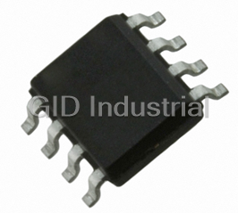
44 PIN TQFP ADAPTER BOARD EPLD
Part Number
ATF15XX-SAA44
Price
Request Quote
Manufacturer
ATMEL
Lead Time
Request Quote
Category
MEMORY & MICROCONTROLLER
Datasheet


Extracted Text
CPLD Development/Programmer Kit .............................................................................................. User Guide -2 CPLD Development/Programmer Kit User Guide xxxxA–XXXXX–xx/xx Table of Contents Section 1 Introduction ........................................................................................... 1-1 1.1 CPLD Development/Programmer Kit ........................................................1-1 1.3 Kit Features...............................................................................................1-2 1.3.1 CPLD Development/Programmer Board ............................................1-2 1.3.2 Logic Doubling CPLDs .......................................................................1-2 1.3.3 CPLD ISP Download Cable................................................................1-2 1.3.4 PLD Software CD-ROM......................................................................1-2 1.3.5 Atmel CD-ROM Data Books ...............................................................1-3 1.4 Device Support .........................................................................................1-3 1.5 System Requirements...............................................................................1-3 1.7 Technical Support .....................................................................................1-4 1.8.1 ProChip Designer ...............................................................................1-5 1.8.2 Atmel-WinCUPL .................................................................................1-5 1.8.3 ATMISP ..............................................................................................1-5 1.8.4 POF2JED ...........................................................................................1-5 Section 2 Hardware Description ........................................................................... 2-1 2.1 Atmel CPLD Development/Programmer Board.........................................2-1 2.1.1 8-segment Display LEDs ....................................................................2-2 2.1.2 Push-button Switches.........................................................................2-6 2.1.3 Clock Select Jumper...........................................................................2-6 2.1.4 VCC Select Jumper ............................................................................2-7 2.1.5 JTAG Port Header ..............................................................................2-7 2.1.6 Power Connectors ..............................................................................2-8 2.2.1 Expansion Terminal Holes..................................................................2-9 2.3 Atmel CPLD ISP Cable .............................................................................2-9 Section 3 CPLD Design Flow Tutorial .................................................................. 3-1 3.1 Overview ...................................................................................................3-1 3.2 Create a Project Using the “New Project Wizard”.....................................3-1 3.3 Add a Design File......................................................................................3-6 Section 4 Schematic Diagrams............................................................................. 4-1 CPLD Development/Programmer Kit User Guide i 3300A–PLD–08/02 Table of Contents ii CPLD Development/Programmer Kit User Guide 3300A–PLD–08/02 Section 1 Introduction 1.1 CPLD The Atmel CPLD Development/Programmer Kit (P/N: ATF15xx-DK2) is a complete development system and an In-System Programming (ISP) programmer for the Development/ ATF15xx family of industry-standard pin-compatible Complex Programmable Logic Programmer Kit ™ Devices (CPLDs) with Logic Doubling features. This kit provides designers a very quick and easy way to develop, prototype and evaluate new designs with an ATF15xx CPLD. With the availability of the different Socket Adapter Boards to support all the package types offered in the ATF15xx family of ISP CPLDs, this CPLD Develop- ment/Programmer Board can be used as an ISP programmer to program the ATF15xx ISP CPLDs in all the available package types through the industry-standard JTAG inter- face (IEEE 1149.1a-1993). Figure 1-1. Contents of the ATF15xx-DK2 CPLD Development/Programmer Kit User Guide 1-1 Rev. 3300A–PLD–08/02 Introduction 1.2 Kit ContentsCPLD Development/Programmer Board (1) 84-lead PLCC Socket Adapter Board (P/N: ATF15xx-SAJ84) Atmel CPLD ISP Download Cable ™ ™ Atmel PLD Software CD-ROM (includes ProChip Designer , Atmel-WinCUPL and other EPLD software) Atmel CD-ROM Data Books One ATF1508AS 5V 84-lead PLCC Sample Device One ATF1508ASVL 3.3V, low-power, 84-lead PLCC Sample Device Atmel CPLD Development/Programmer Kit User Guide Note: 1. Only the 84-lead PLCC Socket Adapter Board is included in this kit. Other Socket Adapter Boards are sold separately. Please refer to Section 1.6 for ordering informa- tion of the Socket Adapter Boards. 1.3 Kit Features 1.3.1 CPLD Development/10-lead JTAG-ISP Port Programmer Board Regulated Power Supply Circuitry for 9V DC Power Source 5V or 3.3V V Operation CC 84-lead PLCC Socket Adapter Board Socket Adapter Board Headers Expansion Terminal Holes for all Input and I/O pins of the ATF15xx Device 2 MHz Crystal Oscillator Eight 8-segment LED Displays Global Clear and Output Enable Push Button Switches 1.3.2 Logic DoublingATF1508AS-15JC84, 5V 128-Macrocell ISP CPLD with Logic Doubling Architecture CPLDs ATF1508ASVL-20JC84, 3.3V Low-power 128-Macrocell ISP CPLD with Logic Doubling Architecture 1.3.3 CPLD ISP Download5V/3.3V ISP Download Cable for PC Parallel Printer (LPT) Port Cable ™ 1.3.4 PLD SoftwareFree Atmel-WinCUPL Design Software CD-ROM ™ 30-day Trial Version of Atmel ProChip Designer Software Full Licensed Version of Atmel ProChip Designer Software (permanent license required) Atmel CPLD ISP Software (ATMISP) POF2JED Conversion Utility Logic Doubling Support and Documentation 1-2 CPLD Development/Programmer Kit User Guide 3300A–PLD–08/02 Introduction 1.3.5 Atmel CD-ROMData Sheets Data Books Application Notes Manuals and User Guides 1.4 Device Support The Atmel CPLD Development/Programmer Board supports the following devices in all speed grades and packages: ATF1502AS/ASL ATF1508AS/ASL ATF1502ASV ATF1508ASV/ASVL ATF1502SE/SEL ATF1508SE/SEL ATF1502AE/AEL ATF1508AE/AEL ATF1504AS/ASL ATF1516SE/SEL (Future) ATF1504ASV/ASVL ATF1516AE/AEL (Future) ATF1504SE/SEL ATF1532AE/AEL (Future) ATF1504AE/AEL 1.5 System The minimum hardware and software requirements to program an ATF15xx ISP CPLD on the CPLD Development/Programmer Board through the Atmel CPLD ISP Software Requirements (ATMISP) V4.0 or later are: ® Pentium or Pentium-compatible microprocessor based computer ® ® Windows 98, Windows NT 4.0, Windows ME, or Windows 2000 16-MByte RAM 10-MByte free hard disk space Windows-supported mouse Available parallel printer (LPT) port 9V DC power supply with 500 mA of supply current SVGA monitor (800 x 600 resolution) CPLD Development/Programmer Kit User Guide 1-3 3300A–PLD–08/02 Introduction 1.6 Ordering Information Part Number Description ATF15xx-DK2 Atmel CPLD Development/Programmer Kit ATF15xx-SAA44 44-lead TQFP Socket Adapter Board ATF15xx-SAJ44 44-lead PLCC Socket Adapter Board ATF15xx-SAC49 49-lead BGA Socket Adapter Board ATF15xx-SAJ68 68-lead PLCC Socket Adapter Board ATF15xx-SAJ84 84-lead PLCC Socket Adapter Board ATF15xx-SAA100 100-lead TQFP Socket Adapter Board ATF15xx-SAQ100 100-lead PQFP Socket Adapter Board ATF15xx-SACT100 100-lead BGA Socket Adapter Board ATF15xx-SAA144 144-lead TQFP Socket Adapter Board ATF15xx-SAQ160 160-lead PQFP Socket Adapter Board ATF15xx-SAC169 169-lead BGA Socket Adapter Board ATF15xx-SAQ208 208-lead PQFP Socket Adapter Board ATF15xx-SACT256 256-lead BGA Socket Adapter Board 1.7 Technical For technical support on any Atmel PLD related issues, please contact the Atmel PLD Applications Group at: Support Hotline: 1-408-436-4333 Email: pld@atmel.com URL: www.atmel.com/atmel 1-4 CPLD Development/Programmer Kit User Guide 3300A–PLD–08/02 Introduction 1.8 References To help PLD designers use the different Atmel PLD software, documentation such as Help Files, Tutorials, Application Notes/Briefs, and User Guides are available. 1.8.1 ProChip Designer ProChip Designer From the ProChip Designer main window, click on HELP and then Help Files select PROCHIP DESIGNER HELP. Tutorials From the ProChip Designer main window, click on HELP and then select TUTORIALS. Known Problems & From the ProChip Designer main window, click on HELP and then Solutions select REVIEW KPS. 1.8.2 Atmel-WinCUPL Help Files From the Atmel-WinCUPL main window, click on HELP and then select CONTENTS. CUPL Programmers From the Atmel-WinCUPL main window, click on HELP and then Reference Guide select CUPL PROGRAMMERS REFERENCE. Tutorial From the Atmel-WinCUPL main window, click on HELP, select ATMEL INFO and then select TUTORIAL1.PDF. Known Problems & From the Atmel-WinCUPL main window, click on HELP, select ATMEL Solutions INFO and then select CUPL_BUG.PDF. 1.8.3 ATMISP Help Files From the ATMISP main window, click on HELP and then select ISP HELP. Tutorial From the ATMISP main window, click on HELP, and then select ATMISP TUTORIAL. Known Problems & Using Windows Explorer, go to the directory where ATMISP is Solutions installed and open the README.TXT file through any ASCII text editor. 1.8.4 POF2JED ATF15xx Conversion From the POF2JED main window, click on HELP and then select Application Brief CONVERSION OPTIONS. CPLD Development/Programmer Kit User Guide 1-5 3300A–PLD–08/02 Introduction 1-6 CPLD Development/Programmer Kit User Guide 3300A–PLD–08/02 Section 2 Hardware Description 2.1 Atmel CPLD The Atmel CPLD Development/Programmer Board, along with the Socket Adapter Board as shown in Figure 2-1, contains many features that designers will find very use- Development/ ful when developing, prototyping, or evaluating their ATF15xx CPLD design. Features Programmer such as push-button switches, 8-segment display LEDs, 2 MHz crystal oscillator, Board 5V/3.3V V selector, JTAG-ISP port, and expansion terminal holes make this a very CC versatile starter/development kit and an ISP programmer for the ATF15xx family of JTAG-ISP CPLDs. Figure 2-1. CPLD Development/Programmer Board with 84-lead PLCC Socket Adapter Board 8-segment Display LEDs 2 MHz Crystal Oscillator Power Supply Clock Select Header Jumper Power Supply Jack Power Switch 84-pin PLCC Power LED Socket Expansion Terminal Holes JTAG Port Header V Select GOE CC GCLR Jumper Push-button Push-button Switch Switch CPLD Development/Programmer Kit User Guide 2-1 Rev. 3300A–PLD–08/02 Hardware Description 2.1.1 8-segment Display The Atmel CPLD Development/Programmer Board contains eight 8-segment LEDs to LEDs allow the designer to observe the outputs of the ATF15xx. These eight LEDs are labeled DSP1 to DSP8 on the board. These eight display LEDs are common anode LEDs with the common anode lines connected to V and the individual cathode lines connected CC to the I/O pins of the ATF15xx CPLD on the CPLD Development/Programmer Board. To turn on a particular segment of an LED, the corresponding ATF15xx I/O pin connected to this LED segment must be in a logical-0 state. Hence, the outputs of the ATF15xx need to be configured as active-low outputs in the design file. Figure 2-2. 8-segment Display LED A B F G E C D Dot Each segment of the display LED is hard-wired to one specific I/O pin of the ATF15xx. For the higher pin count devices (100-lead and larger), all eight segments of the eight LEDs are connected to the I/O pins of the ATF15xx. However, for the lower pin count devices (84-lead and smaller), only a subset of the LED segments are connected to the ATF15xx's I/O pins. Table 2-1 to Table 2-8 below show the connections of the LEDs to the ATF15xx in all the different package types. Table 2-1. Connections of LEDs to ATF15xx 44-lead PLCC DSP/Sgt PLD Pin # DSP/Sgt PLD Pin # DSP/Sgt PLD Pin # DSP/Sgt PLD Pin # 1/A NC 3/A 28 5/A 6 7/A NC 1/B NC 3/B 26 5/B 4 7/B NC 1/C NC 3/C 24 5/C 5 7/C NC 1/D NC 3/D 25 5/D 8 7/D NC 1/E NC 3/E 27 5/E 11 7/E NC 1/F NC 3/F 29 5/F 9 7/F NC 1/G NC 3/G 31 5/G 12 7/G NC 1/DOT NC 3/DOT NC 5/DOT NC 7/DOT NC 2/A NC 4/A 36 6/A 18 8/A NC 2/B NC 4/B 33 6/B 16 8/B NC 2/C NC 4/C 34 6/C 14 8/C NC 2/D NC 4/D 40 6/D 17 8/D NC 2/E NC 4/E 37 6/E 19 8/E NC 2/F NC 4/F 39 6/F 20 8/F NC 2/G NC 4/G 41 6/G 21 8/G NC 2/DOT NC 4/DOT NC 6/DOT NC 8/DOT NC 2-2 CPLD Development/Programmer Kit User Guide 3300A–PLD–08/02 Hardware Description Table 2-2. Connections of LEDs to ATF15xx 44-lead TQFP DSP/Sgt PLD Pin # DSP/Sgt PLD Pin # DSP/Sgt PLD Pin # DSP/Sgt PLD Pin # 1/A NC 3/A 21 5/A 44 7/A NC 1/B NC 3/B 19 5/B 42 7/B NC 1/C NC 3/C 18 5/C 43 7/C NC 1/D NC 3/D 20 5/D 2 7/D NC 1/E NC 3/E 22 5/E 5 7/E NC 1/F NC 3/F 23 5/F 3 7/F NC 1/G NC 3/G 25 5/G 6 7/G NC 1/DOT NC 3/DOT NC 5/DOT NC 7/DOT NC 2/A NC 4/A 30 6/A 12 8/A NC 2/B NC 4/B 27 6/B 10 8/B NC 2/C NC 4/C 28 6/C 8 8/C NC 2/D NC 4/D 34 6/D 11 8/D NC 2/E NC 4/E 31 6/E 13 8/E NC 2/F NC 4/F 33 6/F 14 8/F NC 2/G NC 4/G 35 6/G 15 8/G NC 2/DOT NC 4/DOT NC 6/DOT NC 8/DOT NC Table 2-3. Connections of LEDs to ATF15xx 68-lead PLCC DSP/Sgt PLD Pin # DSP/Sgt PLD Pin # DSP/Sgt PLD Pin # DSP/Sgt PLD Pin # 1/A NC 3/A 47 5/A 5 7/A 25 1/B NC 3/B 45 5/B 4 7/B 24 1/C NC 3/C 44 5/C 7 7/C 27 1/D NC 3/D 46 5/D 9 7/D 29 1/E NC 3/E 49 5/E 13 7/E 32 1/F NC 3/F 51 5/F 8 7/F 28 1/G NC 3/G 52 5/G 10 7/G 30 1/DOT NC 3/DOT NC 5/DOT NC 7/DOT NC 2/A 37 4/A 56 6/A 17 8/A NC 2/B 33 4/B 54 6/B 14 8/B NC 2/C 36 4/C 55 6/C 15 8/C NC 2/D 39 4/D 61 6/D 18 8/D NC 2/E 41 4/E 59 6/E 22 8/E NC 2/F 40 4/F 60 6/F 20 8/F NC 2/G 42 4/G 64 6/G 23 8/G NC 2/DOT NC 4/DOT NC 6/DOT NC 8/DOT NC CPLD Development/Programmer Kit User Guide 2-3 3300A–PLD–08/02 Hardware Description Table 2-4. Connections of LEDs to ATF15xx 84-lead PLCC DSP/Sgt PLD Pin # DSP/Sgt PLD Pin # DSP/Sgt PLD Pin # DSP/Sgt PLD Pin # 1/A 49 3/A 67 5/A 6 7/A 25 1/B 46 3/B 64 5/B 4 7/B 22 1/C 48 3/C 65 5/C 5 7/C 24 1/D 50 3/D 68 5/D 8 7/D 27 1/E 52 3/E 70 5/E 10 7/E 29 1/F 51 3/F 69 5/F 9 7/F 28 1/G 54 3/G 73 5/G 11 7/G 30 1/DOT NC 3/DOT NC 5/DOT 45 7/DOT 41 2/A 57 4/A 76 6/A 16 8/A 34 2/B 55 4/B 74 6/B 12 8/B 31 2/C 56 4/C 75 6/C 15 8/C 33 2/D 58 4/D 77 6/D 17 8/D 35 2/E 61 4/E 80 6/E 20 8/E 37 2/F 60 4/F 79 6/F 18 8/F 36 2/G 63 4/G 81 6/G 21 8/G 39 2/DOT NC 4/DOT NC 6/DOT 44 8/DOT 40 Table 2-5. Connections of LEDs to ATF15xx 100-lead TQFP DSP/Sgt PLD Pin # DSP/Sgt PLD Pin # DSP/Sgt PLD Pin # DSP/Sgt PLD Pin # 1/A 47 3/A 67 5/A 96 7/A 20 1/B 52 3/B 64 5/B 93 7/B 17 1/C 48 3/C 63 5/C 94 7/C 19 1/D 46 3/D 65 5/D 97 7/D 21 1/E 44 3/E 68 5/E 99 7/E 25 1/F 45 3/F 69 5/F 98 7/F 23 1/G 42 3/G 71 5/G 100 7/G 29 1/DOT 49 3/DOT 61 5/DOT 92 7/DOT 22 2/A 54 4/A 80 6/A 12 8/A 32 2/B 41 4/B 76 6/B 9 8/B 30 2/C 40 4/C 78 6/C 8 8/C 31 2/D 56 4/D 84 6/D 10 8/D 33 2/E 58 4/E 81 6/E 13 8/E 36 2/F 57 4/F 83 6/F 14 8/F 35 2/G 60 4/G 85 6/G 16 8/G 37 2/DOT 55 4/DOT 75 6/DOT 6 8/DOT 28 2-4 CPLD Development/Programmer Kit User Guide 3300A–PLD–08/02 Hardware Description Table 2-6. Connections of LEDs to ATF15xx 100-lead PQFP DSP/Sgt PLD Pin # DSP/Sgt PLD Pin # DSP/Sgt PLD Pin # DSP/Sgt PLD Pin # 1/A 48 3/A 69 5/A 98 7/A 22 1/B 50 3/B 66 5/B 95 7/B 19 1/C 49 3/C 65 5/C 96 7/C 21 1/D 47 3/D 67 5/D 99 7/D 23 1/E 44 3/E 70 5/E 3 7/E 27 1/F 46 3/F 71 5/F 100 7/F 25 1/G 43 3/G 73 5/G 4 7/G 39 1/DOT 51 3/DOT 63 5/DOT 94 7/DOT 24 2/A 56 4/A 82 6/A 14 8/A 37 2/B 54 4/B 78 6/B 11 8/B 38 2/C 42 4/C 81 6/C 10 8/C 35 2/D 58 4/D 86 6/D 12 8/D 33 2/E 60 4/E 83 6/E 15 8/E 31 2/F 59 4/F 85 6/F 16 8/F 34 2/G 62 4/G 87 6/G 18 8/G 32 2/DOT 52 4/DOT 77 6/DOT 8 8/DOT 30 Table 2-7. Connections of LEDs to ATF15xx 144-lead TQFP DSP/Sgt PLD Pin # DSP/Sgt PLD Pin # DSP/Sgt PLD Pin # DSP/Sgt PLD Pin # 1/A 79 3/A 100 5/A 134 7/A 25 1/B 78 3/B 98 5/B 137 7/B 22 1/C 74 3/C 99 5/C 136 7/C 23 1/D 80 3/D 101 5/D 133 7/D 26 1/E 82 3/E 106 5/E 138 7/E 28 1/F 81 3/F 102 5/F 132 7/F 27 1/G 83 3/G 107 5/G 131 7/G 29 1/DOT 77 3/DOT 97 5/DOT 139 7/DOT 21 2/A 88 4/A 118 6/A 9 8/A 41 2/B 86 4/B 119 6/B 7 8/B 31 2/C 87 4/C 117 6/C 6 8/C 32 2/D 91 4/D 114 6/D 8 8/D 38 2/E 93 4/E 112 6/E 10 8/E 37 2/F 92 4/F 116 6/F 11 8/F 40 2/G 94 4/G 113 6/G 15 8/G 39 2/DOT 84 4/DOT 111 6/DOT 5 8/DOT 30 CPLD Development/Programmer Kit User Guide 2-5 3300A–PLD–08/02 Hardware Description Table 2-8. Connections of LEDs to ATF15xx 160-lead PQFP DSP/Sgt PLD Pin # DSP/Sgt PLD Pin # DSP/Sgt PLD Pin # DSP/Sgt PLD Pin # 1/A 91 3/A 102 5/A 11 7/A 29 1/B 89 3/B 100 5/B 159 7/B 27 1/C 90 3/C 98 5/C 160 7/C 28 1/D 80 3/D 101 5/D 10 7/D 52 1/E 73 3/E 103 5/E 12 7/E 50 1/F 78 3/F 105 5/F 13 7/F 53 1/G 72 3/G 106 5/G 14 7/G 51 1/DOT 88 3/DOT 97 5/DOT 158 7/DOT 25 2/A 69 4/A 110 6/A 20 8/A 43 2/B 71 4/B 108 6/B 18 8/B 49 2/C 68 4/C 109 6/C 16 8/C 30 2/D 92 4/D 123 6/D 19 8/D 31 2/E 94 4/E 111 6/E 21 8/E 32 2/F 93 4/F 121 6/F 23 8/F 41 2/G 96 4/G 122 6/G 24 8/G 33 2/DOT 70 4/DOT 107 6/DOT 15 8/DOT 48 2.1.2 Push-button Two push-button switches are provided to allow the user to control the logic states of the Switches OE1 and GCLR inputs of the ATF15xx. These two switches are labeled GOE and GCLR on the board. The GCLR push-button switch is a momentary Single-Pole Single-Throw (SPST) normally openswitchwhile theGOE push-buttonswitchis a snap-acting momentary SPST normally open switch. As shown in the CPLD Development/Program- mer Board schematic in Figure 4-1, these two switches are normally open and the GCLR and GOE signals are pulled-up to V when they are not depressed. When the CC switches are depressed, the GCLR and GOE signals are connected to GND. The output of the GCLR switch is connected to the GCLR dedicated input pin of the ATF15xx, and it is intended to be used as an active-low reset signal to reset the regis- ters in the ATF15xx. The output of the GOE switch is connected to the OE1 dedicated input pin of the ATF15xx. It is intended to be used as an active-high or active-low output enable signal to control the enabling/disabling of the tri-state output buffers in the ATF15xx. However, these two switches can also be used to generate general logic input signals to the GCLR and OE1 input pins of the ATF15xx. 2.1.3 Clock Select Jumper The Clock Select Jumper, labeled JPCLK, on the CPLD Development/Programmer Board is a two-position jumper that allows the user to select which GCLK dedicated input pin (either GCLK1 or GCLK2) of the ATF15xx should be connected to the output of the 2 MHz crystal oscillator. In addition, the jumper can be removed to allow an external clock source to be connected to GCLK1 and/or GCLK2 of the ATF15xx. Table 2-9 shows the pin numbers for the GCLR, OE1, GCLK1 and GCLK2 dedicated input pins of the ATF15xx in all the available package types. 2-6 CPLD Development/Programmer Kit User Guide 3300A–PLD–08/02 Hardware Description Table 2-9. Pin Numbers of GCLR, OE1, GCLK1 and GCLK2 44-lead 44-lead 68-lead 84-lead 100-lead 100-lead 144-lead 160-lead Signal TQFP PLCC PLCC PLCC PQFP TQFP TQFP PQFP GCLR 39 1 1 1 91 89 127 141 OE1 384468 849088 126 140 GCLK1 374367 838987 125 139 GCLK2 40 2 2 2 92 90 128 142 2.1.4 V Select Jumper The V Select Jumper, labeled VCC Select, on the CPLD Development/Programmer CC CC Board is a two-position jumper that allows the users to select the V voltage level CC (either 3.3V or 5.0V) used by various components on the CPLD Development/Program- mer Board. This voltage generated by the on-board voltage regulation circuitry is appliedtothe V input pins (both VccINT and VccIO) of the ATF15xx, the common CC anode lines of the eight 8-segment LEDs, the V input of the 2 MHz crystal oscillator, CC the two push-button switches, and the V pin (Pin 4) of the 10-pin JTAG port header CC labeled JTAG. Therefore, when a 3.3V device (ATF15xxASV/ASVL/AE/AEL) is used on this board, the V Select Jumper must be in the 3.3V position. On the other hand, when a 5V device CC (ATF15xxAS/ASL/SE/SEL) is used on this board, the V Select Jumper must be in the CC 5.0V position. This is also true when the ATF15xx is being programmed through ISP on this board. 2.1.5 JTAG Port Header The JTAG Port Header, labeled JTAG, on the CPLD Development/Programmer Board is used to connect the ATF15xx's JTAG port pins (TCK, TDI, TMS and TDO) through the ISP download cable to the parallel printer (LPT) port of a PC for ISP programming of the ATF15xx. Table 2-10 shows the pin numbers for the four JTAG port pins of the ATF15xx in all the available package types. Table 2-10. Pin Numbers of JTAG Port Signals 44-lead 44-lead 68-lead 84-lead 100-lead 100-lead 144-lead 160-lead Signal TQFP PLCC PLCC PLCC PQFP TQFP TQFP PQFP TDI 1 712 146 4 4 9 TDO 323857 717573 104 112 TMS 7 13 19 23 17 15 20 22 TCK 263250 626462 8999 The ISP algorithm is controlled by the ATMISP software, which runs on the PC. The four JTAG signals are generated by the LPT port and they are buffered by the ISP download cable before going into the ATF15xx on the CPLD Development/Programmer Board. The pinout for the 10-pin JTAG Port Header on the CPLD Development/Pro- grammer Board is shown in Figure 2-3 and the dimensions of this 10-pin male JTAG header are shown in Figure 2-4. CPLD Development/Programmer Kit User Guide 2-7 3300A–PLD–08/02 Hardware Description Figure 2-3. Pinout Diagram of 10-pin JTAG Port Header (Top-view) 2 1 TCK GND 4 3 TDO VCC 6 5 NC TMS 8 7 NC NC 9 10 TDI GND Figure 2-4. 10-pin Male Header Dimensions Top View Side View 0.100 0.025 Sq. 0.100 0.235 All dimensions are in inches ® ™ The pinout of this 10-pin JTAG Port Header is compatible with the Altera ByteBlaster ™ and ByteBlasterMV cables. In addition, the ATMISP software allows users to choose either the Atmel CPLD ISP Cable or the ByteBlaster/ByteBlasterMV cable to implement ISP. 2.1.6 Power Connectors The Atmel CPLD Development/Programmer Board contains two different types of power connectors, and either one can be used to connect to a 9V DC power source to power the board. The first power connector, labeled JPower, is a barrel power jack with a 2.1 mm diameter post and it mates to a 2.1 mm (inner diameter) x 5.5 mm (outer diame- ter) female plug. The second power connector, labeled JP Power, is a 4-pin male 0.1" header with 0.025" square posts. The availability of these two types of power connec- tors allows the users to choose the type of power supply equipment to use for the CPLD Development/Programmer Board. 2-8 CPLD Development/Programmer Kit User Guide 3300A–PLD–08/02 Hardware Description 2.2 Socket Adapter Atmel CPLD Development/Programmer Socket Adapter Boards are circuit boards that interface with the Atmel CPLD Development/Programmer Board. They are used in con- Board junction with the CPLD Development/Programmer Board to evaluate/program Atmel ISP CPLDs in different package types. Currently, there are nine Socket Adapter Boards available covering all the package types offered in the ATF15xx family of CPLDs. They include 44-lead PLCC, 44-lead TQFP, 68-lead PLCC, 84-lead PLCC, 100-lead TQFP, 100-lead PQFP, 144-lead TQFP and 160-lead PQFP. New Socket Adapter Boards will become available when new packages are offered. Each socket adapter board contains a socket for the Atmel ATF15xx device on the top side and male headers on the bottom side. The headers on the bottom side mate with the female headers, labeled JPLEFT and JPRIGHT, on the CPLD Development/Pro- grammer Board. The eight 8-segment LEDs, push-button switches, JTAG port signals, crystal oscillator, V , and GND on the CPLD Development/Programmer Board are con- CC nected to the ATF15xx device on the Socket Adapter Board through these two rows of connectors. 2.2.1 Expansion Terminal Rows of expansion terminal holes suitable for 0.1" headers with 0.025" square posts are Holes available on each of the Socket Adapter Boards to allow users to interface the ATF15xx to an external circuit board. All input and I/O pins except the four JTAG port pins of the ATF15xx are routed to these expansion terminal holes, and the corresponding pin num- bers are marked next to the terminal holes. Please refer to the Socket Adapter Board schematics in Section 4 for the pinouts of the expansion terminal holes. On the bottom side of the Socket Adapter Boards, traces connecting the pairs of expan- sion terminal holes can be cut to isolate the LEDs, push-button switches and crystal oscillator from the ATF15xx on the Socket Adapter Board. This allows the users to gain complete control and access to all input and I/O pins of the ATF15xx. 2.3 Atmel CPLD ISP The Atmel CPLD ISP Cable connects the parallel printer (LPT) port of the user’sPCto the 10-pin JTAG header on the Atmel CPLD Development/Programmer Board or a cus- Cable tom circuit board. This is shown in Figure 2-5. This ISP cable acts as a buffer to buffer the JTAG signals between the PC's LPT port and the ATF15xx on the circuit board. The circuit schematic of the Atmel CPLD ISP Cable is shown in Figure 4-10 and Figure 4-11. The Power-On LED on the back of the 25-pin male connector housing indicates that the cable is connected properly. Make sure this LED is turned on before using the Atmel CPLD ISP Software (ATMISP). This ISP cable consists of a 25-pin (DB25) male connector, which is connected to the LPT port of a PC. The 10-pin female plug connects to the 10-pin male JTAG header on the ISP circuit board. The red color stripe on the ribbon cable indicates the orientation of Pin 1 of the female plug. The 10-pin male JTAG header on the CPLD Development/Pro- grammer Board is polarized to prevent users from inserting the female plug in the wrong orientation. If the user is attempting to program low voltage (3.3V) devices, the user needs to use Rev. 4 or later of the Atmel CPLD ISP Cable. This and later revisions will support both the 3.3V and 5V ATF15xx ISP CPLDs. Earlier revisions of the cable only supported 5V devices. When programming 3.3V devices, the V supplied to the ISP cable should also be CC 3.3V. Similarly, the V supplied to the ISP cable should be 5.0V when programming CC 5V devices. CPLD Development/Programmer Kit User Guide 2-9 3300A–PLD–08/02 Hardware Description Figure 2-5. Atmel ISP Cable Connection to ISP Hardware Board/Circuit Board Figure 2-6 shows the pinout for the 10-pin Female header on the Atmel-ISP Cable. The pinout on the 10-pin male header on the PC board (if used for ISP) must match this pinout. Figure 2-6. Atmel ISP Download Cable 10-pin Female Header Pinout Note: The user’s circuit board must supply VCC and GND to the Atmel CPLD ISP Cable through the 10-pin male header (See Figure 2-3). 2-10 CPLD Development/Programmer Kit User Guide 3300A–PLD–08/02 Section 3 CPLD Design Flow Tutorial 3.1 Overview This tutorial will guide the user through a complete design cycle for the Atmel ATF15xx CPLD with Logic Doubling architecture. It will go through each phase of the design cycle step-by-step from design entry, logic synthesis, device fitting, in-system programming, and finally verifying the design on the Atmel CPLD Development/Programming Board. Note: To complete this tutorial, ProChip Designer V4.0 or later and Atmel-ISP Soft- ware (ATMISP) V4.0 or later are required. 3.2 Create a Project Before starting the design process, a Project File must be created within ProChip Designer. ProChip Designer's New Project Wizard provides a very easy way to create Using the “New a new Project File. Project Wizard” 1. Click on the START .... PROGRAMS .... PROCHIP Icon to launch ProChip Designer. Or double-click on the PROCHIP icon on the desktop. (1) Click to launch ProChip Designer CPLD Development/Programmer Kit User Guide 3-1 Rev. 3300A–PLD–08/02 CPLD Design Flow Tutorial 2. Click on PROJECT .... NEW or double-click on the NEW PROJECT shortcut but- ton to launch the New Project Wizard. (2) Click to create New Project 3. Click on the NEXT button to start the project file creation process. (3) Click Next to Start 4. Click on the BROWSE button to open the browser window. 5. Use C:\PROCHIP\DESIGNS\CUPL as the directory of the project. 6. Enter DEV_KIT.APJ as the project filename. The extension of a project file must be .APJ. Note: The name and directory of the design project is specified in this window. All design, simulation and other project files must be placed in this project direc- tory. (4) Click on Browse (5) Select the Project Directory (6) Enter the Project Filename 3-2 CPLD Development/Programmer Kit User Guide 3300A–PLD–08/02 CPLD Design Flow Tutorial 7. Choose [ATF1508AS-10JC84] as the target device type for the project. Also review the Filters that allow for selection of a specific Speed Grade or Package Type. (7) Select the Device Type 8. Select CUPL – ALTIUM as the software tool for this design flow. (8) Select the Design Flow With ProChip Designer V4.0 and later, the five possible design flows and their corre- sponding design entry types supported are listed in the table below: Design Flow Design Entry Type ™ ™ CUPL – Altium CUPL design entry through Altium Protel 99SE ™(1) ® ™ Verilog – Exemplar Verilog design entry through Exemplar Leonardo Spectrum VHDL – Altium VHDL design entry through the Altium PeakFPGA (1) VHDL – Exemplar VHDL design entry through Exemplar Leonardo Spectrum Schematic – Altium Schematic design entry through Altium Protel 99SE ® Note: 1. Design flow require Mentor Graphics Leonardo Spectrum software with Atmel CPLD support. CPLD Development/Programmer Kit User Guide 3-3 3300A–PLD–08/02 CPLD Design Flow Tutorial 9. Select DONE WITH PARTS so that there will be only one device in this project. On the other hand, users can select ADD MORE PARTS to include more parts to the current Project Directory. (9) Select Done with Parts 10. Click the FINISH button to finish the New Project Wizard and the project creation process. This closes the New Project Wizard and opens the ProChip Designer window. The Sources in the project are shown in the Left window. (10) Click Finish to End New Project Wizard 3-4 CPLD Development/Programmer Kit User Guide 3300A–PLD–08/02 CPLD Design Flow Tutorial 11. Click on the Device Icon [ATF1508AS-10JC84] to view the Design Flow window. Project Sources Window Information Dialog Box Message Window (11) Click on the Device Icon Project File Window Design Flow Window CPLD Development/Programmer Kit User Guide 3-5 3300A–PLD–08/02 CPLD Design Flow Tutorial 3.3 Add a Design Once the Project File is created, the next step is to add the design source file(s) into the user’s project. For this tutorial, a single CUPL design file will be added into the project. File 1. Click on the ADD/EDIT button from Source Manager to open the Source Man- ager Window. The user can view the Source Manager Help File by clicking on the Help buttonwithinthe Source Manager Window to view the description for the different processes. 2. In the Source Manager Window, click on the ADD button to add a CUPL design file to the project. 3. In the File Manager Window,select LOGIC_D8.PLD from the C:\PROCHIP\DESIGNS\CUPL directory as the source design file for this project. (1) Click Add/Edit to Open Source Manager Window (3) Select CUPL Source File (2) Click ADD to add Design File This "LOGIC_D8.PLD" is a CUPL design that uses the eight 8-segment LED displays and the 2 MHz oscillator on the Atmel CPLD Development/Programmer Board to gener- ate a scrolling message that displays the words "logic doubling" on the LEDs. The GOE push-button switch is used to control the direction that the message scrolls in (left or right). The GCLR push-button switch is used to reset the counter registers. When the GCLR push-button switch is depressed, the message will stop scrolling. This CUPL design can be compiled using either the ProChip Designer or the Atmel-WinCUPL software. The first section of the LOGIC_D8.PLD as shown below pre-defines which segments of the LED should be asserted in order to display the desired letter or number. For exam- ple, to display the upper case letter "C", segments A, D, E, and F need to be set to low (active low) and the remaining segments need to be set to high. $define Font0 'b'1000000 /* = ( _f_e_d_c_b_a ); 0 */ $define Font1 'b'1111001 /* = ( _c_b ); 1 */ : $define FontA 'b'0001000 /* = (_g_f_e _c_b_a ); A */ 3-6 CPLD Development/Programmer Kit User Guide 3300A–PLD–08/02 CPLD Design Flow Tutorial The next section of this CPLD design as shown below illustrates how to declare and assign pin numbers in the CUPL language to the input and output signals. The input and output pin assignments are assigned according to the connections between the CPLD and the eight 8-segment LED's as shown in the connection tables (Table 2-1 to Table 2- 8) in Section 2. /* Inputs */ pin 1 = GCLR; /* Global Clear input */ pin 83 = MCLK; /* Global Clock input */ pin 84 = GOE; /* GOE1 button used as direction control */ /* Outputs */ /* DSP1 */ pin 49 = LED1A; /* LED1 segment A */ pin 46 = LED1B; /* LED1 segment B */ pin 48 = LED1C; /* LED1 segment C */ pin 50 = LED1D; /* LED1 segment D */ pin 52 = LED1E; /* LED1 segment E */ pin 51 = LED1F; /* LED1 segment F */ pin 54 = LED1G; /* LED1 segment G */ Next, the buried signals for the counter and state machine are declared as PINNODE's as shown below. The feedback and/or the foldback paths available in each macrocell implement these buried signals. For the listing of the pinnode numbers, please refer to the "ATF15xx Device Help" section of the ProChip Designer Help File. pinnode [618,634,650,687]= [CA20..CA17]; pinnode = [CA16..CA0]; pinnode = [SM7..SM0]; After assigning the input, output and buried signals, the related signals (i.e. the LED segments and buried counter) are grouped together as shown below to make the design source code more readable and manageable. In CUPL, the "Field" declaration can be used to group a specific set of signals. Field DSP1 = [LED1G,LED1F,LED1E,LED1D,LED1C,LED1B,LED1A]; Field DSP2 = [LED2G,LED2F,LED2E,LED2D,LED2C,LED2B,LED2A]; : Field CNT_A = [CA20..CA0]; Field SM = [SM7..SM0]; Next, a 21-bit buried up-counter implemented using D-type Flip-flops is shown below 21 and it is used to divide the 2.0 MHz clock into a 0.954 Hz (2 MHz ÷ 2 = 0.954 Hz) sig- nal that can be used to display the text messages. The last bit of this counter is used as the clock for the state machine that controls the display sequence of the messages on the LEDs. CA0.d = !CA0; CA1.d = CA0 $ CA1; : CA7.d = (CA6 & CA5 & CA4 & CA3 & CA2 & CA1 & CA0) $ CA7; : CNT_A.ck = MCLK; CNT_A.ar = !GCLR; CPLD Development/Programmer Kit User Guide 3-7 3300A–PLD–08/02 CPLD Design Flow Tutorial The next section of this PLD design is a state machine with 15 states to control the dis- play sequence of the text messages on the LEDs. The GOE push-button switch on the CPLD Development/Programmer Board controls the flow of this state machine. When this switch is in the "up" position, the state machine will go from RESET to State-0 to State-1 to State-2 and so on until it reaches State-14 and then it will go back to State-0. On the other hand, if the GOE switch is in the "down" position, the state machine will go in the opposite direction (i.e. State-14 to State13 .. etc). SM.ck = COUNTER_1; sequence SM { present RESET next S0; present S0 if SM_DIR next S1; if !SM_DIR next S14; : present S14 if SM_DIR next S0; if !SM_DIR next S13; } Finally, the last section of the PLD design will assign the appropriate letters or numbers to the eight 8-segment LEDs to be displayed during the different states of the state machine. The user can easily change the letters/numbers to be displayed by changing this section of the code to the appropriate pre-defined letters/numbers. LED1 = FontBK & SM:[RESET] # FontBK & SM:[S0] # FontLl & SM:[S1] # FontLo & SM:[S2] # FontLg & SM:[S3] # FontLi & SM:[S4] # FontLc & SM:[S5] # FontBK & SM:[S6] # FontLd & SM:[S7] # FontLo & SM:[S8] # FontLu & SM:[S9] # FontLb & SM:[S10] # FontLl & SM:[S11] # FontLi & SM:[S12] # FontLn & SM:[S13] # FontLg & SM:[S14]; 3-8 CPLD Development/Programmer Kit User Guide 3300A–PLD–08/02 CPLD Design Flow Tutorial 3.4 Compile the In this part of the tutorial, the CUPL design will be compiled through the Logic Synthesis process into a set of optimized/minimized logic equations. CUPL Design 1. Click on the CUPL – Design Ex. button in the Design Flow Window to open the Logic Synthesis Window. (1) Open Logic Synthesis 2. Make sure all of the options in the Optimization section are unchecked. 3. Make sure the Minimization setting is set to Quick. 4. Click on the Compile button to start the CUPL compile process. (2) Make sure these Options are Not Checked (3) Set to Quick (4) Start the Compile Process The user can click on the Set Defaults button and it will automatically specify the Syn- thesis tool in the Tool Text box. If the user clicks on the CUPL Tab, it shows the various Synthesis options. Please refer to the HELP file for further description. CPLD Development/Programmer Kit User Guide 3-9 3300A–PLD–08/02 CPLD Design Flow Tutorial 3.5 Fit the In Section 3.4, the Logic Synthesis portion of the CPLD Design Flow was completed. On successful compilation, the CUPL compiler tool produces a PLA output file (with exten- Synthesized sion .pla). A PLA file contains the netlist of the optimized and minimized logic equations. Design File It is now necessary to map this netlist into a specific Atmel PLD architecture using the Atmel Fitter. 1. The user can now proceed to the Device Fitter portion of the Design Flow by clicking on the Atmel Fitter button. (1) Open the Atmel Fitter Window The user can either use the Default options or specify Fitter properties. ProChip Designer will automatically select the PLA file associated to the current design project and the tool type. In this example, since the target device is an ATF1508AS, the fit1508.exe device fitter will be selected. The fitter creates the important JEDEC and FIT REPORT output files. They contain the data for programming the Device (using In-System Programming or on a third party device programmer) and the pin assignments required for board layout respectively. Please review the Global Device Parameters and Pin/Node Options as well. The Help Files also show the Device Pin_Node lists for each of the ATMEL CPLDs. 2. Make sure the JTAG box is checked. This enables the JTAG port for ISP programming. 3. Make sure the PIN FIT CONTROL setting is set to Keep. This will ensure that the pin assignments in the PLD file will be kept during the Place-and-Route process. 4. When all the fitter options are set, click on the Run Fitter button to fit the design. (2) Check the JTAG box (3)Set the Pin Fit Control setting to KEEP (4) Start the Fitting Process 3-10 CPLD Development/Programmer Kit User Guide 3300A–PLD–08/02 CPLD Design Flow Tutorial The Fitter Report (.FIT) File generated for this design is shown below. Logic Array Block Logic Cells I/O Pins Foldbacks TotalPT FanIN Cascades A: LC1 - LC16 16/16(100%) 8/16(50%) 5/16(31%) 46/80(57%) (19) 0 B: LC17- LC32 16/16(100%) 8/16(50%) 3/16(18%) 51/80(63%) (38) 0 C: LC33- LC48 16/16(100%) 8/16(50%) 2/16(12%) 48/80(60%) (38) 0 D: LC49- LC64 16/16(100%) 6/16(37%) 2/16(12%) 40/80(50%) (38) 0 E: LC65- LC80 16/16(100%) 6/16(37%) 6/16(37%) 55/80(68%) (32) 0 F: LC81- LC96 16/16(100%) 8/16(50%) 2/16(12%) 47/80(58%) (38) 0 G: LC97- LC112 16/16(100%) 8/16(50%) 3/16(18%) 43/80(53%) (25) 0 H: LC113- LC128 16/16(100%) 8/16(50%) 2/16(12%) 42/80(52%) (34) 0 Total dedicated input used: 3/4 (75%) Total I/O pins used 60/64 (93%) Total Logic cells used 128/128 (100%) Total Flip-Flop used 31/128 (24%) Total Foldback logic used 25/128 (19%) Total Nodes+FB/MCells 153/128 (119%) Total cascade used 0 Total input pins 7 Total output pins 56 Total Pts 372 : The ATF15xx Family devices Logic Doubling features provide extra I/O connectivity and logic reusability. Some of the Logic Doubling features available in the ATF15xx family of CPLDs are: Bury either Register or Combinatorial signal while using the other for output Dual independent feedback allows multiple latch functions per macrocell 5 product terms per macrocell, expandable to 40 per macrocell with cascade logic, plus 15 more with foldback logic D/T/Latch configurable flip-flops plus transparent latches Global and/or per macrocell Output Enable Single level Switch Matrix Up to 40 inputs per Logic Block In the LOGIC_D8.PLD example given in this tutorial, Logic Blocks B, C D, and F have 37 or more signal inputs (Fan-In's) as shown in the Universal-Interconnect-Multiplexer assignments section of the .FIT file. The availability of wide Fan-In's to the Logic Blocks is one of the many Logic Doubling features. This feature improves the possibility of rout- ing all the necessary signals from the Global Bus to the Logic Blocks. In addition, macrocells 37 and 59 of the ATF1508 are able to implement both combina- torial outputs (LED1G and LED8D) and buried registered signals (CA0 and RST) within the same macrocells. This is shown in the Resource Usage section of the .FIT file. For more examples of design techniques that utilize the Logic Doubling features of the ATF15xx Family, refer to Atmel's Logic Doubling White Paper and Reference Designs available on the Atmel website. These examples show how to apply Logic Doubling techniques to new product designs, to obtain the benefits of more features in a smaller and possibly less expensive chip, or spare logic resources for future revisions and reduce the risk of PCB re-spin. CPLD Development/Programmer Kit User Guide 3-11 3300A–PLD–08/02 CPLD Design Flow Tutorial 3.6 Program and In this step of the tutorial, the user will program an ATF1508AS 84-pin PLCC device on the Atmel CPLD Development/Programmer Board through ISP and then verify the Verify Design design by observing the text messages displayed on the eight 8-segment LED displays of the CPLD Development/Programmer Board. The user will need to follow the steps below to setup the ATMISP software in order to program the ATF1508AS 84-pin PLCC on the CPLD Development/Programmer Board. 1. To create a new chain file, the ATMISP Software first needs to be launched either through the PROGRAM CHIP button in the ProChip Designer window, the ATMISPdesktopiconorthe Start ... Programs .. Atmel ISP menu. (1) Launch ATMISP If ATMISP is launched through ProChip Designer, steps 2 to 6 below can be skipped since ProChip Designer will automatically setup the appropriate chain file for the ISP operation. 2. To create a new chain file, select the New command under the File menu or click on the New Shortcut Button. (2) Create New Chain File 3. The first piece of information that the software asks for when creating a new chain is the number of devices in the JTAG chain. Therefore, enter 1 and then click OK since a 1-device JTAG chain will be programmed. (3) Enter the number of devices 4. Next the user will need to specify the properties of each JTAG device in the Device Properties window. First, select the target device type of the first device in the JTAG chain. For this tutorial, please select ATF1508AS as the target device type. 5. In the JTAG Instruction field, the user can specify the appropriate JTAG instruc- tion to be executed on this device in the chain. Please select Program/Verify to program and verify the ATF1508AS. 3-12 CPLD Development/Programmer Kit User Guide 3300A–PLD–08/02 CPLD Design Flow Tutorial 6. The next step is to specify the JEDEC file to be programmed into the target device in the JEDEC File field. Click on the Browse button, change the directory to [..\PROCHIP\DESIGNS\CUPL"] and then select LOGIC_D8.JED as the tar- get JEDEC file. Click OK to close the JTAG Device Properties window when all properties are specified. (5) Specify JTAG Instruction (4) Specify Target Device Type (6) Select JEDEC File The next few steps require the user to setup the Atmel CPLD Development/Programmer Board to program the ATF1508AS through ISP. 7. Connect the 25-DB side of the Atmel-ISP Cable to the PC's parallel port and the 10-pin header side of the Atmel-ISP Cable to the Atmel CPLD Development Board as shown Figure 2-5. 8. Connect a 9V AC/DC power adapter to the power connector (JPower) of the Atmel CPLD Development/Programmer Board. 9. Set the 5V/3.3V jumper to 5V. This will set the system board V to 5V. CC 10. Set the JPCLK jumper to GCLK1 so that the output of the crystal oscillator will be connected to Pin 83 of the ATF1508AS. 11. Connect the 84-pin PLCC Socket Adapter Board onto the main Develop- ment/Programmer Board. Note: If a device in a different package type is to be programmed, then the appropriate Socket Adapter Board must be used. 12. Switch the Power Switch to the ON position. 13. Select the appropriate LPT port in the Port Setting field. LPT 1 is the default port. 14. Select the ISP download cable type in the Cable Types field. The default cable type is the Atmel ISP Cable but it can be changed to the Altera ByteBlaster cable if the ByteBlaster cable is being used. Now both the user’s software and hardware are setup for ISP programming, and the user can execute the PROGRAM/VERIFY instruction to program the ATF1508AS on the Atmel CPLD Development/Programmer Board. CPLD Development/Programmer Kit User Guide 3-13 3300A–PLD–08/02 CPLD Design Flow Tutorial 15. Click on the Run button in the ATMISP main window to execute the JTAG instruction to program the ATF1508AS on the CPLD Development/Programmer Board. (13) Select LPT Port Number (14) Select Cable Type (15) Click on the RUN Button After successfully programming the ATF1508AS with the LOGIC_D8.JED file, the eight 8-segment LED's will display the words "Logic Doubling". If these two text messages are correctly displayed on the CPLD Development/Program- mer Board, then the user has successfully completed this tutorial. 3-14 CPLD Development/Programmer Kit User Guide 3300A–PLD–08/02 Section 4 Schematic Diagrams CPLD Development/Programmer Kit User Guide 4-1 Rev. 3300A–PLD–08/02 JPRIGHT JPRIGHT VCC VCC GND GND 1 2 GCLK1 GCLK1 GCLK2 GCLK2 3 4 D4G D4G D4D D4D 5 6 D4F D4F D4E D4E 7 8 D4A D4A D4C D4C 9 10 10 RDOT1 RDOT1 RDOT2 RDOT2 RDOT3 RDOT3 RDOT4 RDOT4 RDOT5 RDOT5 RDOT6 RDOT6 RDOT7 RDOT7 RDOT8 RDOT8 D4B D4B DOT4 DOT4 11 11 12 12 D3G D3G TDO TDO 13 13 14 14 D3F D3F D3E D3E 15 15 16 16 D3A D3A D3D D3D 17 17 18 18 D3B D3B D3C D3C 19 19 20 20 DSP1 DSP1 DSP2 DSP2 DSP3 DSP3 DSP4 DSP4 DSP5 DSP5 DSP6 DSP6 DSP7 DSP7 DSP8 DSP8 TCK TCK DOT3 DOT3 VCC VCC 21 21 22 22 D2G D2G D2E D2E 23 23 24 24 D2F D2F D2D D2D 25 25 26 26 D2A D2A D2C D2C 27 27 28 28 D2B D2B DOT2 DOT2 29 29 30 30 D1G D1G D1E D1E a a a a a a a a 31 31 32 32 D1F D1F D1D D1D b b b b b b b b 33 33 34 34 f f f f f f f f D1A D1A D1C D1C g g g g g g g g 35 35 36 36 D1B D1B DOT1 DOT1 37 37 38 38 GND GND VCC VCC 39 39 40 40 e c e c e c e c e c e c e c e c d d d d d d d d HEADER HEADER 20X2 20X2 JPLEFT JPLEFT VCC VCC GND GND 1 2 GOE GOE GCLR GCLR 3 4 D5B D5B DOT5 DOT5 5 6 D5A D5A D5C D5C 7 8 D5F D5F D5D D5D 9 10 10 D5G D5G D5E D5E 11 11 12 12 DOT6 DOT6 TDI TDI 13 13 14 14 D6B D6B D6C D6C 15 15 16 16 D6A D6A D6D D6D 17 17 18 18 D6F D6F D6E D6E 19 19 20 20 D6G D6G TMS TMS 21 21 22 22 D7B D7B DOT7 DOT7 23 23 24 24 D7A D7A D7C D7C 25 25 26 26 D7F D7F D7D D7D 27 27 28 28 D7G D7G D7E D7E JPCLK JPCLK 29 29 30 30 VCC VCC D8B D8B DOT8 DOT8 31 31 32 32 D8A D8A D8C D8C 33 33 34 34 D8F D8F D8D D8D 35 35 36 36 D8G D8G D8E D8E GCLK2 GCLK2 GCLK1 GCLK1 37 37 38 38 GND GND VCC VCC R7 R7 R8 R8 R R 9 9 R10 R10 39 39 40 40 4.7K 4.7K 4.7K 4.7K 10K 10K 4.7K 4.7K HEADER HEADER 20X2 20X2 R5 R5 R6 R6 R11 R11 R12 R12 VR1 VR1 VCC VCC JTAG JTAG 1K 1K 1K 1K 1K 1K 1K 1K LM317 LM317 TCK TCK 1 2 3 2 TDO TDO Vin Vin +Vout +Vout 3 4 TMS TMS 5 6 GCLR GCLR GOE GOE 7 8 TDI TDI C3 C3 9 10 10 R1 R1 0.1 0.1 R4 R4 JP JP JP JP Power Power OSC OSC 200 200 1K 1K 1 4 GCLR GCLR GOE1 GOE1 2 3 2MHZ 2MHZ R2 R2 LED1 LED1 VCC VCC D1 D1 POWER POWER SWITCH SWITCH 330 330 9 1N4001 1N4001 V JPower JPower C5 C5 C6 C6 C7 C7 R3 R3 C C 2 2 C1 C1 0.1uF 0.1uF 0.1uF 0.1uF 0.1uF 0.1uF 0.1uF 0.1uF 100uF 100uF 270 270 5.0V 5.0V 3.3V 3.3V Vcc Vcc Select Select Schematic Diagrams Figure 4-1. Schematic Diagram of the Atmel CPLD Development/Programmer Board 1 2 3 4 D1A D1A RDSP11 RDSP11 a Vc1 Vc1 D1B D1B RDSP12 RDSP12 b 1 D1C D1C RDSP13 RDSP13 ADJ ADJ c D1D D1D RDSP14 RDSP14 d Vc2 Vc2 RDSP15 RDSP15 D1E D1E e D1F D1F RDSP16 RDSP16 f RDSP17 RDSP17 D1G D1G DOT1 DOT1 g DOT DOT RDSP21 RDSP21 D2A D2A 3 a Vc1 Vc1 D2B D2B RDSP22 RDSP22 2 b RDSP23 RDSP23 D2C D2C 1 c D2D D2D RDSP24 RDSP24 d Vc2 Vc2 RDSP25 RDSP25 D2E D2E e RDSP26 RDSP26 D2F D2F f D2G D2G RDSP27 RDSP27 DOT2 DOT2 g DOT DOT RDSP31 RDSP31 D3A D3A a Vc1 Vc1 D3B D3B RDSP32 RDSP32 b D3C D3C RDSP33 RDSP33 c RDSP34 RDSP34 D3D D3D d Vc2 Vc2 D3E D3E RDSP35 RDSP35 e D3F D3F RDSP36 RDSP36 f RDSP37 RDSP37 D3G D3G DOT3 DOT3 g DOT DOT D4A D4A RDSP41 RDSP41 a Vc1 Vc1 RDSP42 RDSP42 D4B D4B b D4C D4C RDSP43 RDSP43 c D4D D4D RDSP44 RDSP44 d Vc2 Vc2 D4E D4E RDSP45 RDSP45 e D4F D4F RDSP46 RDSP46 f RDSP47 RDSP47 D4G D4G DOT4 DOT4 g DOT DOT RDSP51 RDSP51 D5A D5A a Vc1 Vc1 D5B D5B RDSP52 RDSP52 b D5C D5C RDSP53 RDSP53 c D5D D5D RDSP54 RDSP54 d Vc2 Vc2 RDSP55 RDSP55 D5E D5E e RDSP56 RDSP56 D5F D5F f D5G D5G RDSP57 RDSP57 DOT5 DOT5 g DOT DOT D6A D6A RDSP61 RDSP61 a Vc1 Vc1 D6B D6B RDSP62 RDSP62 b D6C D6C RDSP63 RDSP63 c RDSP64 RDSP64 D6D D6D d Vc2 Vc2 D6E D6E RDSP65 RDSP65 e RDSP66 RDSP66 D6F D6F f RDSP67 RDSP67 D6G D6G DOT6 DOT6 g DOT DOT D7A D7A RDSP71 RDSP71 a Vc1 Vc1 RDSP72 RDSP72 D7B D7B b D7C D7C RDSP73 RDSP73 c D7D D7D RDSP74 RDSP74 d Vc2 Vc2 RDSP75 RDSP75 D7E D7E e D7F D7F RDSP76 RDSP76 f D7G D7G RDSP77 RDSP77 DOT7 DOT7 5 6 g DOT DOT 3 4 1 2 RDSP81 RDSP81 D8A D8A a Vc1 Vc1 D8B D8B RDSP82 RDSP82 b RDSP83 RDSP83 D8C D8C c D8D D8D RDSP84 RDSP84 d Vc2 Vc2 D8E D8E RDSP85 RDSP85 5 6 e RDSP86 RDSP86 D8F D8F 3 4 f D8G D8G RDSP87 RDSP87 DOT8 DOT8 1 2 g DOT DOT 1 2 3 4-2 CPLD Development/Programmer Kit User Guide 3300A–PLD–08/02 JPLEFT VCC GND 1 2 GOE GCLR 3 4 D5B 5 6 D5A D5C 7 8 D5F D5D 9 10 D5G D5E 11 12 TDI 13 14 D6B D6C 15 16 D6A D6D 17 18 D6F D6E 19 20 D6G TMS 21 22 23 24 U1 25 26 27 28 TDI 7 39 P39 D4F TDI I/O P8 29 30 D5D 8 38 TDO I/O TDO P9 31 32 D5F 9 37 P37 D4E I/O I/O 33 34 GND 10 36 P36 D4A GND I/O P11 35 36 D5E 11 35 VCC I/O VCC P12 37 38 D5G 12 34 P34 D4C GND VCC I/O I/O 39 40 TMS 13 ATMEL PLCC44 33 P33 D4B TMS I/O P14 D6C 14 32 TCK HEADER 20X2 I/O TCK VCC 15 31 P31 D3G VCC I/O P16 D6B 16 30 GND JPRIGHT I/O GND P17 D6D 17 29 P29 D3F VCC GND I/O I/O 1 2 GCLK1 GCLK2 3 4 D4G D4D PLCC44 5 6 D4F D4E 7 8 D4A D4C 9 10 D4B 11 12 D3G TDO 13 14 D3F D3E 15 16 D3A D3D 17 18 D3B D3C 19 20 VCC TCK 21 22 23 24 25 26 27 28 29 30 c1 c2 c3 c4 31 32 0.1uF 0.1uF 0.1uF 0.1uF 33 34 35 36 37 38 GND VCC 39 40 HEADER 20X2 Schematic Diagrams Figure 4-2. Schematic Diagram of 44-pin PLCC Socket Adapter Board P18 D6A 18 6 D5A P6 I/O I/O P19 D6E 19 5 D5C P5 I/O I/O P20 D6F 20 4 D5B P4 I/O I/O P21 D6G 21 3 VCC I/O VCC GND 22 2 GCLK2 P2 GND I/OE2/GCLK2 VCC 23 1 GCLR P1 VCC GCLR P24 D3C 24 44 GOE P44 I/O OE1 P25 D3D 25 43 GCLK1 P43 I/O GCLK1 P26 D3B 26 42 GND I/O GND P27 D3E 27 41 P41 D4G I/O GCLK3 P28 D3A 28 40 P40 D4D I/O I/O CPLD Development/Programmer Kit User Guide 4-3 3300A–PLD–08/02 JPLEFT VCC GND 1 2 GOE GCLR 3 4 D5B 5 6 D5A D5C 7 8 D5F D5D 9 10 D5G D5E 11 12 TDI 13 14 D6B D6C 15 16 D6A D6D 17 18 D6F D6E 19 20 D6G TMS 21 22 U1 23 24 25 26 TDI 1 33 P33 D4F TDI I/O P2 27 28 D5D 2 32 TDO I/O TDO P3 29 30 D5F 3 31 P31 D4E I/O I/O 31 32 GND 4 30 P30 D4A GND I/O P5 33 34 D5E 5 29 VCC I/O VCC P6 35 36 D5G 6 28 P28 D4C I/O I/O 37 38 TMS 7 ATMEL TQFP44 27 P27 D4B GND VCC TMS I/O P8 39 40 D6C 8 26 TCK I/O TCK VCC 9 25 P25 D3G HEADER 20X2 VCC I/O P10 D6B 10 24 GND I/O GND P11 JPRIGHT D6D 11 23 P23 D3F I/O I/O VCC GND 1 2 GCLK1 GCLK2 3 4 TQFP44 D4G D4D 5 6 D4F D4E 7 8 D4A D4C 9 10 D4B 11 12 D3G TDO 13 14 D3F D3E 15 16 D3A D3D 17 18 D3B D3C VCC 19 20 TCK 21 22 23 24 25 26 27 28 c1 c2 c3 c4 29 30 0.1uF 0.1uF 0.1uF 0.1uF 31 32 33 34 35 36 37 38 GND VCC 39 40 HEADER 20X2 Schematic Diagrams Figure 4-3. Schematic Diagram of 44-pin TQFP Socket Adapter Board P12 D6A 12 44 D5A P44 I/O I/O P13 D6E 13 43 D5C P43 I/O I/O P14 D6F 14 42 D5B P42 I/O I/O P15 D6G 15 41 VCC I/O VCC GND 16 40 GCLK2 P40 GND I/OE2/GCLK2 VCC 17 39 GCLR P39 VCC GCLR P18 D3C 18 38 GOE P38 I/O OE1 P19 D3B 19 37 GCLK1 P37 I/O GCLK1 P20 D3D 20 36 GND I/O GND P21 D3A 21 35 P35 D4G I/O GCLK3 P22 D3E 22 34 P34 D4D I/O I/O 4-4 CPLD Development/Programmer Kit User Guide 3300A–PLD–08/02 JPLEFT VCC GND 1 2 GOE GCLR 3 4 D5B 5 6 D5A D5C 7 8 D5F D5D 9 10 D5G D5E 11 12 TDI 13 14 D6B D6C 15 16 D6A D6D U1 17 18 D6F D6E 19 20 D6G TMS D5G 10 60 P60 D4F P10 21 22 I/O I/O D7B VCC 11 59 P59 D4E 23 24 VCC I/O D7A D7C TDI 12 58 GND 25 26 TDI GND D7F D7D D5E 13 57 TDO P13 27 28 I/O TDO D7G D7E D6B 14 56 P56 D4A P14 29 30 I/O I/O D6C 15 55 P55 D4C P15 31 32 I/O I/O GND 16 54 P54 D4B 33 34 GND I/O D6A 17 53 VCC P17 35 36 I/O VCC D6D 18 52 P52 D3G P18 37 38 I/O ATMEL PLCC68 I/O GND VCC TMS 19 51 P51 D3F 39 40 TMS I/O D6F 20 50 TCK P20 I/O TCK HEADER 20X2 VCC 21 49 P49 D3E VCC I/O D6E 22 48 GND P22 I/O GND JPRIGHT D6G 23 47 P47 D3A P23 I/O I/O VCC GND D7B 24 46 P46 D3D P24 1 2 I/O I/O GCLK1 GCLK2 D7A 25 45 P45 D3B P25 3 4 I/O I/O D4G D4D GND 26 44 P44 D3C 5 6 GND I/O D4F D4E 7 8 D4A D4C 9 10 D4B 11 12 D3G TDO 13 14 D3F D3E 15 16 D3A D3D 17 18 D3B D3C VCC 19 20 TCK 21 22 D2G D2E 23 24 D2F D2D 25 26 D2A D2C 27 28 c1 c2 c3 c4 D2B 29 30 0.1uF 0.1uF 0.1uF 0.1uF 31 32 33 34 35 36 37 38 GND VCC 39 40 HEADER 20X2 Schematic Diagrams Figure 4-4. Schematic Diagram of 68-pin PLCC Socket Adapter Board P27 D7C 27 9 P9 D5D I/O I/O P28 D7F 28 8 P8 D5F I/O I/O P29 D7D 29 7 P7 D5C I/O I/O P30 D7G 30 6 GND I/O GND VCC 31 5 D5A P5 VCC I/O D7E P32 32 4 D5B P4 I/O I/O D2B P33 33 3 VCC I/O VCC GND 34 2 GCLK2 P2 GND GCLK2 VCC 35 1 GCLR P1 VCC GCLR P36 D2C 36 68 P68 GOE I/O OE1 P37 D2A 37 67 GCLK1 P67 I/O GCLK1 GND 38 66 GND GND GND P39 D2D 39 65 P65 I/O GCLK3 P40 D2F 40 64 D4G P64 I/O I/O P41 D2E 41 63 VCC I/O VCC P42 D2G 42 62 P62 I/O TCK VCC 43 61 D4D P61 VCC I/O CPLD Development/Programmer Kit User Guide 4-5 3300A–PLD–08/02 JPRIGHT VCC GND 1 2 JR1 JR2 PIN83 GCLK1 GCLK2 PIN2 3 4 JR3 JR4 MARK PIN81 D4G D4D PIN77 5 6 JR5 JR6 SMALLATMEL PIN79 D4F D4E PIN80 7 8 JR7 JR8 PIN76 D4A D4C PIN75 9 10 JR9 JR10 PIN74 D4B 11 12 JR11 PIN73 D3G TDO 13 14 JR12 JR13 PIN69 D3F D3E PIN70 15 16 JR14 JR16 U1 PIN67 D3A D3D PIN68 17 18 JR15 JR17 PIN64 D3B D3C PIN65 19 20 JR19 TCK 21 22 JR18 JR21 PIN12 12 74 PIN74 PIN63 D2G D2E PIN61 I/O I/O 23 24 JR20 JR22 VCC 13 73 PIN73 PIN60 D2F D2D PIN58 VCC_IO I/O 25 26 JR23 JR24 TDI 14 72 GND PIN57 D2A D2C PIN56 I/O / TDI GND 27 28 JR25 JR26 PIN15 15 71 TDO PIN55 D2B I/O I/O / TDO 29 30 JR27 JR28 PIN16 16 70 PIN70 PIN54 D1G D1E PIN52 I/O I/O 31 32 JR29 JR30 PIN17 17 69 PIN69 PIN51 D1F D1D PIN50 I/O I/O 33 34 JR31 JR32 PIN18 18 68 PIN68 PIN49 D1A D1C PIN48 I/O I/O JR33 35 36 JR34 GND 19 67 PIN67 PIN46 D1B GND I/O 37 38 PIN20 20 66 VCC GND VCC I/O VCC_IO 39 40 PIN21 21 ATMEL 65 PIN65 I/O I/O HEADER 20X2 PIN22 22 64 PIN64 I/O I/O TMS 23 63 PIN63 I/O / TMS I/O PIN24 24 ATF1508AS-15JC84 62 TCK JPLEFT I/O I/O / TCK PIN25 25 61 PIN61 VCC GND I/O I/O 1 2 JL1 JL2 VCC 26 60 PIN60 PIN84 GOE GCLR PIN1 VCC_IO I/O JL3 3 4 JL4 PIN27 27 59 GND PIN4 D5B DOT5 PIN45 I/O GND 5 6 JL5 JL6 PIN28 28 58 PIN58 PIN6 D5A D5C PIN5 I/O I/O 7 8 JL7 JL8 PIN29 29 57 PIN57 PIN9 D5F D5D PIN8 I/O I/O 9 10 JL9 JL10 PIN30 30 56 PIN56 PIN11 D5G D5E PIN10 I/O I/O 11 12 JL11 PIN31 31 55 PIN55 PIN44 DOT6 TDI I/O I/O 13 14 JL12 JL13 GND 32 54 PIN54 PIN12 D6B D6C PIN15 GND I/O 15 16 JL14 JL15 PIN16 D6A D6D PIN17 17 18 JL16 JL17 VCC PIN18 D6F D6E PIN20 19 20 JL18 PIN21 D6G TMS 21 22 JL19 JL20 PIN22 D7B DOT7 PIN41 JL21 23 24 JL22 PIN25 D7A D7C PIN24 25 26 JL23 JL24 PIN28 D7F D7D PIN27 27 28 JL25 JL26 c1 c2 c3 c4 PIN30 D7G D7E PIN29 29 30 JL27 JL28 0.1uF 0.1uF 0.1uF 0.1uF PIN31 D8B DOT8 PIN40 31 32 JL29 JL30 PIN34 D8A D8C PIN33 33 34 JL31 JL32 PIN36 D8F D8D PIN35 35 36 JL33 JL34 PIN39 D8G D8E PIN37 37 38 GND VCC 39 40 HEADER 20X2 Schematic Diagrams Figure 4-5. Schematic Diagram of 84-pin PLCC Socket Adapter Board PIN33 33 11 PIN11 I/O I/O PIN34 34 10 PIN10 I/O I/O PIN35 35 9 PIN9 I/O I/O PIN36 36 8 PIN8 I/O I/O PIN37 37 7 GND I/O GND VCC 38 6 PIN6 VCC_IO I/O PIN39 39 5 PIN5 I/O I/O PIN40 40 4 PIN4 I/O I/O PIN41 41 3 VCC I/O VCC_INT GND 42 2 PIN2 GND INPUT/OE2/GCLK2 VCC 43 1 PIN1 VCC_INT INPUT/GCLRn PIN44 44 84 PIN84 I/O INPUT/OE1 PIN45 45 83 PIN83 I/O INPUT/GCLK1 PIN46 46 82 GND I/O GND GND 47 81 PIN81 GND I/O PIN48 48 80 PIN80 I/O I/O PIN49 49 79 PIN79 I/O I/O PIN50 50 78 VCC I/O VCC_IO PIN51 51 77 PIN77 I/O I/O PIN52 52 76 PIN76 I/O I/O VCC 53 75 PIN75 VCC_IO I/O 4-6 CPLD Development/Programmer Kit User Guide 3300A–PLD–08/02 JPLEFT VCC GND 1 2 GOE GCLR 3 4 D5B DOT5 5 6 D5A D5C 7 8 D5F D5D 9 10 D5G D5E 11 12 DOT6 TDI 13 14 D6B D6C 15 16 D6A D6D 17 18 D6F D6E 19 20 U1 D6G TMS 21 22 D7B DOT7 23 24 1 80 D7A D7C P1 P80 I/On I/On 25 26 2 79 D7F D7D P2 P79 I/On I/On 27 28 D5E 3 78 D4B D7G D7E P3 P78 I/O I/O 29 30 D5G 4 77 DOT4 D8B DOT8 P4 P77 I/O I/O 31 32 VCC 5 76 GND D8A D8C VCCIO GND 33 34 TDI 6 75 TDO D8F D8D TDI TDO 35 36 P7 7 74 D8G D8E P74 I/On I/On 37 38 DOT6 P8 8 73 D3G GND VCC P73 I/O I/O 39 40 P9 9 72 P72 I/On I/On D6C P10 10 71 D3F HEADER 20X2 P71 I/O I/O D6B P11 11 70 D3E P70 I/O I/O D6D P12 12 69 D3A P69 I/O I/O GND 13 68 VCC JPRIGHT GND VCCIO D6A P14 14 67 D3D VCC GND P67 I/O I/O 1 2 D6E P15 15 66 D3B GCLK1 GCLK2 P66 I/O I/O 3 4 D6F P16 16 ATMEL PQFP100 65 D3C D4G D4D P65 I/O I/O 5 6 TMS 17 64 TCK D4F D4E TMS TCK 7 8 D6G P18 18 63 DOT3 D4A D4C P63 I/O I/O 9 10 D7B P19 19 62 D2G D4B DOT4 P62 I/O I/O 11 12 VCC 20 61 GND D3G TDO VCCIO GND 13 14 D7C P21 21 60 D2E D3F D3E P60 I/O I/O 15 16 D7A P22 22 59 D2F D3A D3D P59 I/O I/O 17 18 D7D P23 23 58 D2D D3B D3C P58 I/O I/O 19 20 DOT7 P24 24 57 TCK DOT3 P57 I/On I/On 21 22 D7F P25 25 56 D2A D2G D2E P56 I/O I/O 23 24 P26 26 55 D2F D2D P55 I/On I/On 25 26 D7E P27 27 54 D2B D2A D2C P54 I/O I/O 27 28 GND 28 53 VCC D2B DOT2 GND VCCIO 29 30 P29 29 52 DOT2 D1G D1E P52 I/On I/On 31 32 DOT8 P30 30 51 DOT1 D1F D1D P51 I/On I/On 33 34 D1A D1C 35 36 D1B DOT1 37 38 GND VCC 39 40 VCC HEADER 20X2 c1 c2 c3 c4 0.1uF 0.1uF 0.1uF 0.1uF Schematic Diagrams Figure 4-6. Schematic Diagram of 100-pin PQFP Socket Adapter Board D8E 31 100 P100 D5F P31 I/O I/O D8G 32 99 P99 D5D P32 I/O I/O D8D 33 98 P98 D5A P33 I/O I/O D8F 34 97 GND P34 I/O GND D8C 35 96 P96 D5C P35 I/O I/O VCC 36 95 P95 D5B VCCIO I/O D8A 37 94 P94 DOT5 P37 I/O I/O D8B 38 93 VCC P38 I/O VCCINT D7G 39 92 P92 GCLK2 P39 I/O GCLK2 GND 40 91 P91 GCLR GND GCLR VCC 41 90 P90 GOE VCCINT OE1 D2C 42 89 P89 GCLK1 P42 I/O GCLK1 D1G 43 88 GND P43 I/O GND D1E 44 87 P87 D4G P44 I/O I/O/GCLK3 GND 45 86 P86 D4D GND I/O D1F 46 85 P85 D4F P46 I/O I/O D1D 47 84 VCC P47 I/O VCCIO D1A 48 83 P83 D4E P48 I/O I/O D1C 49 82 P82 D4A P49 I/O I/O D1B 50 81 P81 D4C P50 I/O I/O CPLD Development/Programmer Kit User Guide 4-7 3300A–PLD–08/02 JPLEFT VCC GND 1 2 GOE GCLR 3 4 D5B DOT5 5 6 D5A D5C 7 8 D5F D5D 9 10 U1 D5G D5E 11 12 DOT6 TDI 13 14 1 75 DOT4 P1 P75 D6B D6C I/On I/O 15 16 2 74 GND P2 D6A D6D I/On GND 17 18 VCC 3 73 TDO D6F D6E VCCIO TDO 19 20 TDI 4 72 P72 D6G TMS TDI I/On 21 22 5 71 D3G P5 P71 D7B DOT7 I/On I/O 23 24 DOT6 6 70 P6 P70 D7A D7C I/O I/On 25 26 7 69 D3F P7 P69 D7F D7D I/On I/O 27 28 D6C 8 68 D3E P8 P68 D7G D7E I/O I/O 29 30 D6B 9 67 D3A P9 P67 D8B DOT8 I/O I/O 31 32 D6D 10 66 VCC P10 D8A D8C I/O VCCIO 33 34 GND 11 65 D3D P65 D8F D8D GND I/O 35 36 D6A 12 64 D3B P12 P64 D8G D8E I/O I/O 37 38 D6E 13 ATMEL TQFP100 63 D3C P13 P63 GND VCC I/O I/O 39 40 D6F 14 62 TCK P14 I/O TCK TMS 15 61 DOT3 P61 HEADER 20X2 TMS I/O D6G 16 60 D2G P16 P60 I/O I/O D7B 17 59 GND P17 I/O GND JPRIGHT VCC 18 58 D2E P58 VCCIO I/O VCC GND D7C 19 57 D2F P19 P57 1 2 I/O I/O GCLK1 GCLK2 D7A 20 56 D2D P20 P56 3 4 I/O I/O D4G D4D D7D 21 55 DOT2 P21 P55 5 6 I/O I/On D4F D4E DOT7 22 54 D2A P22 P54 7 8 I/On I/O D4A D4C D7F 23 53 P23 P53 9 10 I/O I/On D4B DOT4 24 52 D1B P24 P52 11 12 I/On I/O D3G TDO D7E 25 51 VCC P25 13 14 I/O VCCIO D3F D3E 15 16 D3A D3D 17 18 D3B D3C TQFP100 19 20 TCK DOT3 21 22 D2G D2E VCC 23 24 D2F D2D 25 26 D2A D2C 27 28 D2B DOT2 29 30 D1G D1E 31 32 c1 c2 c3 c4 D1F D1D 33 34 0.1uF 0.1uF 0.1uF 0.1uF D1A D1C 35 36 D1B DOT1 37 38 GND VCC 39 40 HEADER 20X2 Schematic Diagrams Figure 4-7. Schematic Diagram of 100-pin TQFP Socket Adapter Board P100 GND 26 100 D5G GND I/O P27 P99 27 99 D5E I/On I/O P28 P98 DOT8 28 98 D5F I/On I/O P29 P97 D7G 29 97 D5D I/O I/O P30 P96 D8B 30 96 D5A I/O I/O P31 D8C 31 95 GND I/O GND P32 P94 D8A 32 94 D5C I/O I/O P33 P93 D8D 33 93 D5B I/O I/O P92 VCC 34 92 DOT5 VCCIO I/O P35 D8F 35 91 VCC I/O VCCINT P36 P90 D8E 36 90 GCLK2 I/O GCLK2 P37 P89 D8G 37 89 GCLR I/O GCLR P88 GND 38 88 GOE GND OE1 P87 VCC 39 87 GCLK1 VCCINT GCLK1 P40 D2C 40 86 GND I/O GND P41 P85 D2B 41 85 D4G I/O I/O GCLK3 P42 P84 D1G 42 84 D4D I/O I/O P83 GND 43 83 D4F GND I/O P44 D1E 44 82 VCC I/O VCCIO P45 P81 D1F 45 81 D4E I/O I/O P46 P80 D1D 46 80 D4A I/O I/O P47 P79 D1A 47 79 I/O I/On P48 P78 D1C 48 78 D4C I/O I/O P49 P77 DOT1 49 77 I/On I/On P50 P76 50 76 D4B I/On I/O 4-8 CPLD Development/Programmer Kit User Guide 3300A–PLD–08/02 JPLEFT VCC GND 1 2 GOE GCLR 3 4 D5B DOT5 5 6 D5A D5C 7 8 D5F D5D 9 10 D5G D5E 11 12 DOT6 TDI 13 14 D6B D6C 15 16 D6A D6D 17 18 D6F D6E 19 20 D6G TMS 21 22 D7B DOT7 23 24 D7A D7C 25 26 D7F D7D U1 27 28 D7G D7E 29 30 D8B DOT8 1 108 31 32 I/On I/On D8A D8C 2 107 P107 D3G 33 34 I/On I/O D8F D8D GND 3 106 P106 D3E 35 36 GND I/O D8G D8E TDI 4 105 GND 37 38 TDI GND GND VCC P5 DOT6 5 104 TDO 39 40 I/O TDO P6 D6C 6 103 I/O I/On HEADER 20X2 P7 D6B 7 102 P102 D3F I/O I/O P8 D6D 8 101 P101 D3D I/O I/O P9 D6A 9 100 P100 D3A I/O I/O JPRIGHT P10 D6E 10 99 P99 D3C I/O I/O VCC GND P11 D6F 11 98 P98 D3B 1 2 I/O I/O GCLK1 GCLK2 12 97 P97 DOT3 3 4 I/On I/O D4G D4D GND 13 96 P96 5 6 GND I/O D4F D4E P14 14 95 VCC 7 8 I/O VCCIO D4A D4C P15 D6G 15 94 P94 D2G 9 10 I/O I/O D4B DOT4 P16 16 93 P93 D2E 11 12 I/O I/O D3G TDO GND 17 92 P92 D2F 13 14 GND I/O D3F D3E P18 18 91 P91 D2D 15 16 I/O I/O D3A D3D 19 90 17 18 I/On I/On D3B D3C TMS 20 89 TCK 19 20 TMS TCK TCK DOT3 P21 DOT7 21 ATMEL TQFP144 88 P88 D2A 21 22 I/O I/O D2G D2E P22 D7B 22 87 P87 D2C 23 24 I/O I/O D2F D2D P23 D7C 23 86 P86 D2B 25 26 I/O I/O D2A D2C VCC 24 85 GND 27 28 VCCIO GND D2B DOT2 P25 D7A 25 84 P84 DOT2 29 30 I/O I/O D1G D1E P26 D7D 26 83 P83 D1G 31 32 P27 I/O I/O D1F D1D D7F 27 82 P82 D1E 33 34 I/O I/O D1A D1C P28 D7E 28 81 P81 D1F 35 36 I/O I/O D1B DOT1 P29 D7G 29 80 P80 D1D 37 38 I/O I/O GND VCC P30 DOT8 30 79 P79 D1A 39 40 I/O I/O P31 D8B 31 78 P78 D1B HEADER 20X2 I/O I/O D8C P32 32 77 P77 DOT1 I/O I/O GND 33 76 VCC GND VCCIO 34 75 I/On I/On VCC 35 74 P74 D1C I/On I/O 36 73 VCC I/On VCCIO TQFP144 c1 c2 c3 c4 0.1uF 0.1uF 0.1uF 0.1uF Schematic Diagrams Figure 4-8. Schematic Diagram of 144-pin TQFP Socket Adapter Board D8E P37 37 144 VCC I/O VCCIO D8D P38 38 143 P143 I/O I/O D8G P39 39 142 P142 I/O I/O D8F P40 40 141 P141 I/O I/O D8A P41 41 140 P140 I/O I/O P42 42 139 DOT5 P139 I/O I/O 43 138 D5E P138 I/On I/O P44 44 137 D5B P137 I/O I/O P45 45 136 D5C P136 I/O I/O 46 135 GND I/On GND 47 134 D5A P134 I/On I/O 48 133 D5D P133 I/On I/O 49 132 D5F P132 I/On I/O VCC 50 131 D5G P131 VCCIO I/O VCC 51 130 VCC VCCINT VCCINT GND 52 129 GND GND GND P53 53 128 GCLK2 P128 I/O GCLK2 P54 54 127 GCLR P127 I/O GCLR P55 55 126 GOE P126 I/O GOE P56 56 125 GCLK1 P125 I/O GCLK GND 57 124 GND GND GND VCC 58 123 VCC VCCINT VCINT GND 59 122 GND I/On P60 60 121 I/O I/On P61 61 120 I/O I/On P119 P62 62 119 D4B I/O I/O P63 63 118 D4A P118 I/O I/O GND 64 117 D4C P117 GND I/O P65 65 116 D4F P116 I/O I/O 66 115 VCC I/On VCCIO P67 67 114 D4D P114 I/O I/O P68 68 113 D4G P113 I/O I/O P69 69 112 D4E P112 I/O I/O P70 70 111 DOT4 P111 I/O I/O P71 71 110 P110 I/O I/O P72 72 109 P109 I/O I/O CPLD Development/Programmer Kit User Guide 4-9 3300A–PLD–08/02 JPLEFT VCC GND 1 2 GOE GCLR 3 4 D5B DOT5 5 6 D5A D5C 7 8 D5F D5D 9 10 D5G D5E 11 12 DOT6 TDI 13 14 D6B D6C 15 16 D6A D6D 17 18 D6F D6E 19 20 D6G TMS 21 22 D7B DOT7 23 24 U1 D7A D7C 25 26 D7F D7D 27 28 1 120 D7G D7E NC NC 29 30 2 119 D8B DOT8 NC NC 31 32 3 118 D8A D8C NC NC 33 34 4 117 D8F D8D NC NC 35 36 5 116 D8G D8E NC NC 37 38 6 115 GND VCC NC NC 39 40 7 114 NC NC VCC 8 113 GND HEADER 20X2 VCCIO GND TDI 9 112 TDO TDI TDO P111 D5D P10 10 111 D4E I/O I/O D5A P11 11 110 P110 D4A JPRIGHT I/O I/O D5E P12 12 109 P109 D4C VCC GND I/O I/O 1 2 D5F P13 13 108 P108 D4B GCLK1 GCLK2 I/O I/O 3 4 D5G P14 14 107 P107 DOT4 D4G D4D I/O I/O 5 6 DOT6 P15 15 106 P106 D3G D4F D4E I/O I/O 7 8 D6C P16 16 105 P105 D3F D4A D4C I/O I/O 9 10 GND 17 104 VCC D4B DOT4 GND VCCIO 11 12 D6B P18 18 103 P103 D3E D3G TDO I/O I/O 13 14 D6D P19 19 102 P102 D3A D3F D3E I/O I/O 15 16 D6A P20 20 101 P101 D3D D3A D3D I/O I/O 17 18 D6E P21 21 ATMEL PQFP160 100 P100 D3B D3B D3C I/O I/O 19 20 TMS 22 99 TCK TCK DOT3 TMS TCK 21 22 D6F P23 23 98 P98 D3C D2G D2E I/O I/O 23 24 D6G P24 24 97 P97 DOT3 D2F D2D I/O I/O 25 26 DOT7 P25 25 96 P96 D2G D2A D2C I/O I/O 27 28 VCC 26 95 GND D2B DOT2 VCCIO GND 29 30 D7B P27 27 94 P94 D2E D1G D1E I/O I/O 31 32 D7C P28 28 93 P93 D2F D1F D1D I/O I/O 33 34 D7A P29 29 92 P92 D2D D1A D1C I/O I/O 35 36 D8C P30 30 91 P91 D1A D1B DOT1 I/O I/O 37 38 D8D P31 31 90 P90 D1C GND VCC I/O I/O 39 40 D8E P32 32 89 P89 D1B I/O I/O HEADER 20X2 D8G P33 33 88 P88 DOT1 I/O I/O 34 87 NC NC 35 86 NC NC 36 85 VCC NC NC 37 84 NC NC 38 83 NC NC 39 82 NC NC 40 81 NC NC c1 c2 c3 c4 0.1uF 0.1uF 0.1uF 0.1uF Schematic Diagrams Figure 4-9. Schematic Diagram of 160-pin PQFP Socket Adapter Board D8F P41 41 160 P160 D5C I/O I/O GND 42 159 P159 D5B GND I/O D8A 43 158 P158 DOT5 P43 I/O I/O 44 157 NC NC 45 156 NC NC 46 155 NC NC 47 154 NC NC DOT8 48 153 P153 P48 I/O I/O D8B 49 152 P152 P49 I/O I/O D7E P50 50 151 P151 I/O I/O D7G 51 150 P150 P51 I/O I/O D7D 52 149 P149 P52 I/O I/O D7F P53 53 148 GND I/O GND P54 54 147 P147 I/O I/O VCC 55 146 P146 VCCIO I/O 56 145 P145 P56 I/O I/O 57 144 P144 P57 I/O I/O P58 58 143 VCC I/O VCCINT 59 142 P142 GCLK2 P59 I/O GCLK2 GND 60 141 P141 GCLR GND GCLR VCC 61 140 P140 GOE VCCINT OE1 P62 62 139 P139 GCLK1 I/O GCLK1 63 138 GND P63 I/O GND 64 137 P137 P64 I/O I/O/GCLK3 65 136 P136 P65 I/O I/O GND 66 135 P135 GND I/O 67 134 P134 P67 I/O I/O D2C P68 68 133 VCC I/O VCCIO D2A 69 132 P132 P69 I/O I/O DOT2 P70 70 131 P131 I/O I/O D2B P71 71 130 P130 I/O I/O D1G 72 129 P129 P72 I/O I/O D1E 73 128 P128 P73 I/O I/O 74 127 NC NC 75 126 NC NC 76 125 NC NC 77 124 NC NC D1F P78 78 123 P123 D4D I/O I/O VCC 79 122 P122 D4G VCCIO I/O D1D 80 121 P121 D4F P80 I/O I/O 4-10 CPLD Development/Programmer Kit User Guide 3300A–PLD–08/02 Buffer/Line Driver VCC D1 R16 100 TCK 1N4148 R17 100 R26 R25 R24 R23 R22 R21 AF 4.7k 4.7k 4.7k 4.7k 4.7k 4.7k R18 100 TDI U1 2 18 R19 100 STROBE 1A1 1Y1 4 16 AUTO 1A2 1Y2 INI 6 14 D0 1A3 1Y3 8 12 R20 100 INIT 1A4 1Y4 11 9 SEL_IN 2A1 2Y1 TMS 13 7 TDO 2A2 2Y2 15 5 D7 2A3 2Y3 17 3 VCC 2A4 2Y4 nACK 1 20 1G VCC 19 10 2G GND BUSY C1 74VHC244 20-SOIC 0.1uF GND GND VCC JP1 TCK 1 2 TDO 3 4 TMS 5 6 INI 7 8 AF TDI 9 10 HEADER 5X2 R1 330ohm GND L1 LED 10 Pin Header to ISP Board GND Schematic Diagrams Figure 4-10. Schematic Diagram of Atmel CPLD ISP Cable CPLD Development/Programmer Kit User Guide 4-11 3300A–PLD–08/02 Parallel Port Section Voltage Detection VCC R2 100 STROBE R3 100 AUTO R12 10K 1.36V at VCC = 3.3 R13 4.7K P1 R4 100 2.06V at VCC = 5.0 1 D0 1.5V - 1.6V Vref 14 2 15 ERROR 3 100 R5 16 D2 1N4148 INIT 4 17 SEL_IN 5 R6 100 18 VCC 6 R14 3.3K D3 1N4148 19 7 20 R7 100 8 D7 21 D4 1N4148 VCC 9 R8 100 22 nACK 10 4 8 4 8 23 R9 100 11 LM393 U2A LM393 U2B BUSY 8-SOP 8-SOP 24 12 VCC GND R15 30K 25 R10 4.7K 13 R11 4.7K ERROR DB25 3V = 0 GND 5V = 1 GND Schematic Diagrams Figure 4-11. Schematic Diagram of Atmel CPLD ISP Cable, Continued 2 1 3 6 7 5 4-12 CPLD Development/Programmer Kit User Guide 3300A–PLD–08/02 + - + - Atmel Headquarters Atmel Operations Corporate Headquarters Memory RF/Automotive 2325 Orchard Parkway 2325 Orchard Parkway Theresienstrasse 2 San Jose, CA 95131 San Jose, CA 95131 Postfach 3535 TEL 1(408) 441-0311 TEL 1(408) 441-0311 74025 Heilbronn, Germany FAX 1(408) 487-2600 FAX 1(408) 436-4314 TEL (49) 71-31-67-0 FAX (49) 71-31-67-2340 Europe Microcontrollers Atmel Sarl 2325 Orchard Parkway 1150 East Cheyenne Mtn. Blvd. Route des Arsenaux 41 San Jose, CA 95131 Colorado Springs, CO 80906 Case Postale 80 TEL 1(408) 441-0311 TEL 1(719) 576-3300 CH-1705 Fribourg FAX 1(408) 436-4314 FAX 1(719) 540-1759 Switzerland Biometrics/Imaging/Hi-Rel MPU/ TEL (41) 26-426-5555 La Chantrerie FAX (41) 26-426-5500 BP 70602 High Speed Converters/RF Datacom 44306 Nantes Cedex 3, France Avenue de Rochepleine Asia TEL (33) 2-40-18-18-18 BP 123 Room 1219 FAX (33) 2-40-18-19-60 38521 Saint-Egreve Cedex, France Chinachem Golden Plaza TEL (33) 4-76-58-30-00 ASIC/ASSP/Smart Cards 77 Mody Road Tsimshatsui FAX (33) 4-76-58-34-80 East Kowloon Zone Industrielle Hong Kong 13106 Rousset Cedex, France TEL (852) 2721-9778 TEL (33) 4-42-53-60-00 FAX (852) 2722-1369 FAX (33) 4-42-53-60-01 Japan 1150 East Cheyenne Mtn. Blvd. 9F, Tonetsu Shinkawa Bldg. Colorado Springs, CO 80906 1-24-8 Shinkawa TEL 1(719) 576-3300 Chuo-ku, Tokyo 104-0033 FAX 1(719) 540-1759 Japan TEL (81) 3-3523-3551 Scottish Enterprise Technology Park FAX (81) 3-3523-7581 Maxwell Building East Kilbride G75 0QR, Scotland TEL (44) 1355-803-000 FAX (44) 1355-242-743 e-mail literature@atmel.com Web Site http://www.atmel.com © Atmel Corporation 2002. Atmel Corporation makes no warranty for the use of its products, other than those expressly contained in the Company’s standard warranty whichisdetailedinAtmel’s Terms and Conditions located on the Company’s web site. The Company assumes no responsibility for any errors which may appear in this document, reserves the right to change devices or specifications detailed herein at any time without notice, and does not make any commitment to update the information contained herein. No licenses to patents or other intellectual property of Atmel are granted by the Company in connection with the sale of Atmel products, expressly or by implication. Atmel’s products are not authorized for use as critical components in life support devices or systems. ® ™ ™ ™ ATMEL is the registered trademark of Atmel; Logic Doubling , ProChip Designer and Atmel-WinCUPL are the trademarks of Atmel. ® ™ ™ Altera is the registered trademark of Altera Corporation; ByteBlaster and ByteBlasterMV are the trade- ® ® marks of Altera Corporation. Pentium is the registered trademark of Intel Corporation. Windows and Win- ® ® dows NT are the registered trademarks of Microsoft Corporation. Verilog is a registered trademark of Printed on recycled paper. ® Cadence Design Systems, Inc. Mentor Graphics is a registered trademark of Mentor Graphics Corporation; ™ ™ ® ™ Exemplar and Leonardo Spectrum are trademarks of Mentor Graphics Corporation. Altium ,PeakFPGA ™ 3300A–PLD–08/02 /1M and Protel are trademarks and registered trademarks of Altium Limited. Other terms and product names may be the trademarks of others.
Frequently asked questions
What makes Elite.Parts unique?

What kind of warranty will the ATF15XX-SAA44 have?
Which carriers does Elite.Parts work with?
Will Elite.Parts sell to me even though I live outside the USA?
I have a preferred payment method. Will Elite.Parts accept it?








What they say about us
FANTASTIC RESOURCE
One of our top priorities is maintaining our business with precision, and we are constantly looking for affiliates that can help us achieve our goal. With the aid of GID Industrial, our obsolete product management has never been more efficient. They have been a great resource to our company, and have quickly become a go-to supplier on our list!
Bucher Emhart Glass
EXCELLENT SERVICE
With our strict fundamentals and high expectations, we were surprised when we came across GID Industrial and their competitive pricing. When we approached them with our issue, they were incredibly confident in being able to provide us with a seamless solution at the best price for us. GID Industrial quickly understood our needs and provided us with excellent service, as well as fully tested product to ensure what we received would be the right fit for our company.
Fuji
HARD TO FIND A BETTER PROVIDER
Our company provides services to aid in the manufacture of technological products, such as semiconductors and flat panel displays, and often searching for distributors of obsolete product we require can waste time and money. Finding GID Industrial proved to be a great asset to our company, with cost effective solutions and superior knowledge on all of their materials, it’d be hard to find a better provider of obsolete or hard to find products.
Applied Materials
CONSISTENTLY DELIVERS QUALITY SOLUTIONS
Over the years, the equipment used in our company becomes discontinued, but they’re still of great use to us and our customers. Once these products are no longer available through the manufacturer, finding a reliable, quick supplier is a necessity, and luckily for us, GID Industrial has provided the most trustworthy, quality solutions to our obsolete component needs.
Nidec Vamco
TERRIFIC RESOURCE
This company has been a terrific help to us (I work for Trican Well Service) in sourcing the Micron Ram Memory we needed for our Siemens computers. Great service! And great pricing! I know when the product is shipping and when it will arrive, all the way through the ordering process.
Trican Well Service
GO TO SOURCE
When I can't find an obsolete part, I first call GID and they'll come up with my parts every time. Great customer service and follow up as well. Scott emails me from time to time to touch base and see if we're having trouble finding something.....which is often with our 25 yr old equipment.
ConAgra Foods