

 Manufacturers
ATMEL AT93C46-10SI-1.8
Description
Atmel AT93C46-10SI-1.8 Integrated Circuit. EEPROM | 1KBIT | 2 MHZ | 8 SOIC
Part Number
AT93C46-10SI-1.8
Price
Request Quote
Manufacturer
ATMEL
Lead Time
Request Quote
Category
MEMORY & MICROCONTROLLER
Specifications
Interface
Microwire, 3-Wire Serial
Lead Free Status
Contains Lead
Memory Size
1K (128 x 8 or 64 x 16)
Memory Type
EEPROM
Operating Temperature
-40°C ~ 85°C
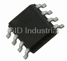
Package / Case
8-SOIC (0.154", 3.90mm Width)
Packaging
Tube
RoHS Status
RoHS Non-Compliant
Speed
250kHz, 1MHz, 2MHz
Voltage - Supply
1.8 V ~ 5.5 V
Features
- 2 MHz Clock Rate (5V)
- 8-lead PDIP, 8-lead JEDEC SOIC, 8-lead EIAJ SOIC, 8-lead MAP, 8-lead TSSOP, and 8-ball dBGA2™ Packages
- Automotive Grade, Extended Temperature and Lead-Free/Halogen-Free
- Devices Available
- High Reliability
- Low-voltage and Standard-voltage Operation
- Self-timed Write Cycle (10 ms max)
- Three-wire Serial Interface
- User-selectable Internal Organization
Datasheet

Extracted Text
Features • Low-voltage and Standard-voltage Operation –2.7 (V = 2.7V to 5.5V) CC –1.8 (V = 1.8V to 5.5V) CC User-selectable Internal Organization – 1K: 128 x 8 or 64 x 16 – 2K: 256 x 8 or 128 x 16 – 4K: 512 x 8 or 256 x 16 Three-wire Serial Interface 2 MHz Clock Rate (5V) Self-timed Write Cycle (10 ms max) Three-wire High Reliability – Endurance: 1 Million Write Cycles Serial – Data Retention: 100 Years Automotive Grade, Extended Temperature and Lead-Free/Halogen-Free EEPROMs Devices Available 8-lead PDIP, 8-lead JEDEC SOIC, 8-lead EIAJ SOIC, 8-lead MAP, 8-lead TSSOP, ™ 1K (128 x 8 or 64 x 16) and 8-ball dBGA2 Packages 2K (256 x 8 or 128 x 16) Description 4K (512 x 8 or 256 x 16) The AT93C46/56/66 provides 1024/2048/4096 bits of serial electrically erasable pro- grammable read-only memory (EEPROM), organized as 64/128/256 words of 16 bits each (when the ORG pin is connected to VCC), and 128/256/512 words of 8 bits each (when the ORG pin is tied to ground). The device is optimized for use in many indus- AT93C46 trial and commercial applications where low-power and low-voltage operations are (1) essential. The AT93C46/56/66 is available in space-saving 8-lead PDIP, 8-lead AT93C56 JEDEC SOIC, 8-lead EIAJ SOIC, 8-lead MAP, 8-lead TSSOP, and 8-lead dBGA2™ (2) packages. AT93C66 The AT93C46/56/66 is enabled through the Chip Select pin (CS) and accessed via a three-wire serial interface consisting of Data Input (DI), Data Output (DO), and Shift Clock (SK). Upon receiving a Read instruction at DI, the address is decoded and the data is clocked out serially on the DO pin. The Write cycle is completely self-timed, Note: 1. This device is not recom- mended for new designs. and no separate Erase cycle is required before Write. The Write cycle is only enabled Please refer to AT93C56A. when the part is in the Erase/Write Enable state. When CS is brought high following the initiation of a Write cycle, the DO pin outputs the Ready/Busy status of the part. 2. This device is not recom- mended for new designs. The AT93C46/56/66 is available in 2.7V to 5.5V and 1.8V to 5.5V versions. Please refer to AT93C66A. Table 1. Pin Configurations 8-lead SOIC 8-lead dBGA2 Pin Name Function 8 1 CS 1 8 VCC VCC CS CS Chip Select 7 2 SK SK 2 7 DC DC ORG 6 3 D1 DI 3 6 ORG SK Serial Data Clock GND 5 4 D0 DO 4 5 GND DI Serial Data Input 8-lead SOIC 8-lead PDIP Rotated (R) (1K JEDEC Only) DO Serial Data Output CS 1 8 VCC DC 1 8 ORG SK 2 7 DC GND Ground VCC 2 7 GND DI 3 6 ORG CS 3 6 DO DO 4 5 GND VCC Power Supply SK 4 5 DI ORG Internal Organization 8-lead MAP 8-lead TSSOP DC Don’t Connect CS 1 8 VCC VCC 8 1 CS SK 2 7 DC 7 2 DC SK DI 3 6 ORG 6 3 ORG DI DO 4 5 GND 5 4 GND DO Rev. 0172Y–SEEPR–11/04 1 Absolute Maximum Ratings* *NOTICE: Stresses beyond those listed under “Absolute Operating Temperature......................................−55°C to +125°C Maximum Ratings” may cause permanent dam- age to the device. This is a stress rating only, and Storage Temperature .........................................−65°C to +150°C functional operation of the device at these or any Voltage on Any Pin other conditions beyond those indicated in the with Respect to Ground........................................ −1.0V to +7.0V operational sections of this specification is not implied. Exposure to absolute maximum rating Maximum Operating Voltage .......................................... 6.25V conditions for extended periods may affect device reliability DC Output Current........................................................ 5.0 mA Figure 1. Block Diagram Note: When the ORG pin is connected to VCC, the “x 16” organization is selected. When it is connected to ground, the “x 8” organization is selected. If the ORG pin is left uncon- nected and the application does not load the input beyond the capability of the internal 1 Meg ohm pullup, then the “x 16” organization is selected. The feature is not available on the 1.8V devices. For the AT93C46, if “x 16” organization is the mode of choice and Pin 6 (ORG) is left unconnected, Atmel recommends using the AT93C46A device. For more details, see the AT93C46A datasheet. 2 AT93C46/56/66 0172Y–SEEPR–11/04 AT93C46/56/66 (1) Table 2. Pin Capacitance Applicable over recommended operating range from T = 25°C, f = 1.0 MHz, V = +5.0V (unless otherwise noted) A CC Symbol Test Conditions Max Units Conditions C Output Capacitance (DO) 5 pF V = 0V OUT OUT C Input Capacitance (CS, SK, DI) 5 pF V = 0V IN IN Note: 1. This parameter is characterized and is not 100% tested. Table 3. DC Characteristics Applicable over recommended operating range from: T = −40°C to +85°C, V = +1.8V to +5.5V, AI CC T = -40°C to +125°C, V = +1.8V to +5.5V (unless otherwise noted) AE CC Symbol Parameter Test Condition Min Typ Max Unit V Supply Voltage 1.8 5.5 V CC1 V Supply Voltage 2.7 5.5 V CC2 V Supply Voltage 4.5 5.5 V CC3 READ at 1.0 MHz 0.5 2.0 mA I Supply Current V = 5.0V CC CC WRITE at 1.0 MHz 0.5 2.0 mA I Standby Current V = 1.8V CS = 0V 0 0.1 µA SB1 CC I Standby Current V = 2.7V CS = 0V 6.0 10.0 µA SB2 CC I Standby Current V = 5.0V CS = 0V 17 30 µA SB3 CC I Input Leakage V = 0V to V 0.11.0µA IL IN CC I Output Leakage V = 0V to V 0.11.0µA OL IN CC (1) V Input Low Voltage −0.6 0.8 IL1 2.7V ≤ V ≤ 5.5V V CC (1) V Input High Voltage 2.0 V + 1 IH1 CC (1) V Input Low Voltage −0.6 V x 0.3 IL2 CC 1.8V ≤ V ≤ 2.7V V CC (1) V Input High Voltage V x 0.7 V + 1 IH2 CC CC V Output Low Voltage I = 2.1 mA 0.4 V OL1 OL 2.7V ≤ V ≤ 5.5V CC V Output High Voltage I = −0.4 mA 2.4 V OH1 OH V Output Low Voltage I = 0.15 mA 0.2 V OL2 OL 1.8V ≤ V ≤ 2.7V CC V Output High Voltage I = −100 µA V – 0.2 V OH2 OH CC Note: 1. V min and V max are reference only and are not tested. IL IH 3 0172Y–SEEPR–11/04 Table 4. AC Characteristics Applicable over recommended operating range from T = −40°C to + 85°C, V = As Specified, AI CC CL = 1 TTL Gate and 100 pF (unless otherwise noted) Symbol Parameter Test Condition Min Typ Max Units 4.5V ≤ V ≤ 5.5V 0 2 CC SK Clock f 2.7V ≤ V ≤ 5.5V 0 1 MHz SK CC Frequency 1.8V ≤ V ≤ 5.5V 0 0.25 CC 4.5V ≤ V ≤ 5.5V 250 CC t SK High Time 2.7V ≤ V ≤ 5.5V 250 ns SKH CC 1.8V ≤ V ≤ 5.5V 1000 CC 4.5V ≤ V ≤ 5.5V 250 CC t SK Low Time 2.7V ≤ V ≤ 5.5V 250 ns SKL CC 1.8V ≤ V ≤ 5.5V 1000 CC 4.5V ≤ V ≤ 5.5V 250 CC Minimum CS t 2.7V ≤ V ≤ 5.5V 250 ns CS CC Low Time 1.8V ≤ V ≤ 5.5V 1000 CC 4.5V ≤ V ≤ 5.5V 50 CC t CS Setup Time Relative to SK 2.7V ≤ V ≤ 5.5V 50 ns CSS CC 1.8V ≤ V ≤ 5.5V 200 CC 4.5V ≤ V ≤ 5.5V 100 CC t DI Setup Time Relative to SK 2.7V ≤ V ≤ 5.5V 100 ns DIS CC 1.8V ≤ V ≤ 5.5V 400 CC t CS Hold Time Relative to SK 0 ns CSH 4.5V ≤ V ≤ 5.5V 100 CC t DI Hold Time Relative to SK 2.7V ≤ V ≤ 5.5V 100 ns DIH CC 1.8V ≤ V ≤ 5.5V 400 CC 4.5V ≤ V ≤ 5.5V 250 CC Output Delay to t AC Test 2.7V ≤ V ≤ 5.5V 250 ns PD1 CC “1” 1.8V ≤ V ≤ 5.5V 1000 CC 4.5V ≤ V ≤ 5.5V 250 CC Output Delay to t AC Test 2.7V ≤ V ≤ 5.5V 250 ns PD0 CC “0” 1.8V ≤ V ≤ 5.5V 1000 CC 4.5V ≤ V ≤ 5.5V 250 CC CS to Status t AC Test 2.7V ≤ V ≤ 5.5V 250 ns SV CC Valid 1.8V ≤ V ≤ 5.5V 1000 CC 4.5V ≤ V ≤ 5.5V 100 CC CS to DO in High AC Test t 2.7V ≤ V ≤ 5.5V 100 ns DF CC Impedance CS = V IL 1.8V ≤ V ≤ 5.5V 400 CC 10 ms t Write Cycle Time WP 4.5V ≤ V ≤ 5.5V 0.1 3 ms CC (1) Endurance 5.0V, 25°C 1M Write Cycles Note: 1. This parameter is characterized and is not 100% tested. 4 AT93C46/56/66 0172Y–SEEPR–11/04 AT93C46/56/66 Table 5. Instruction Set for the AT93C46 Address Data Op Instruction SB Code x 8 x 16 x 8 x 16 Comments Reads data stored in memory, at READ 1 10 A – A A – A 6 0 5 0 specified address Write enable must precede all EWEN 1 00 11XXXXX 11XXXX programming modes – A A – A Erases memory location A – A ERASE 1 11 A 6 0 5 0 n 0 WRITE 1 01 A – A A – A D – D D – D Writes memory location A – A 6 0 5 0 7 0 15 0 n 0 Erases all memory locations. Valid ERAL 1 00 10XXXXX 10XXXX only at V = 4.5V to 5.5V CC Writes all memory locations. Valid WRAL 1 00 01XXXXX 01XXXX D – D D – D 7 0 15 0 only at V = 4.5V to 5.5V CC EWDS 1 00 00XXXXX 00XXXX Disables all programming instructions Note: The Xs in the address field represent DON’T CARE values and must be clocked. (1) (2) Table 6. Instruction Set for the AT93C56 and AT93C66 Address Data Op Instruction SB Code x 8 x 16 x 8 x 16 Comments Reads data stored in memory, at READ 1 10 A – A A – A 8 0 7 0 specified address Write enable must precede all EWEN 1 00 11XXXXXXX 11XXXXXX programming modes – A A – A Erases memory location A – A ERASE 1 11 A 8 0 7 0 n 0 WRITE 1 01 A – A A – A D – D D – D Writes memory location A – A 8 0 7 0 7 0 15 0 n 0 Erases all memory locations. Valid ERAL 1 00 10XXXXXXX 10XXXXXX only at V = 4.5V to 5.5V CC Writes all memory locations. Valid WRAL 1 00 01XXXXXXX 01XXXXXX D – D D – D only at V = 5.0V ±10% and Disable 7 0 15 0 CC Register cleared EWDS 1 00 00XXXXXXX 00XXXXXX Disables all programming instructions Note: 1. This device is not recommended for new designs. Please refer to AT93C56A. 2. This device is not recommended for new designs. Please refer to AT93C66A. 5 0172Y–SEEPR–11/04 Functional The AT93C46/56/66 is accessed via a simple and versatile three-wire serial communi- cation interface. Device operation is controlled by seven instructions issued by the host Description processor. A valid instruction starts with a rising edge of CS and consists of a start bit (logic “1”) followed by the appropriate op code and the desired memory address location. READ (READ): The Read (READ) instruction contains the address code for the mem- ory location to be read. After the instruction and address are decoded, data from the selected memory location is available at the serial output pin DO. Output data changes are synchronized with the rising edges of serial clock SK. It should be noted that a dummy bit (logic “0”) precedes the 8- or 16-bit data output string. ERASE/WRITE ENABLE (EWEN): To assure data integrity, the part automatically goes into the Erase/Write Disable (EWDS) state when power is first applied. An Erase/Write Enable (EWEN) instruction must be executed first before any programming instructions can be carried out. Please note that once in the EWEN state, programming remains enabled until an EWDS instruction is executed or V power is removed from the part. CC ERASE (ERASE): The Erase (ERASE) instruction programs all bits in the specified memory location to the logical “1” state. The self-timed erase cycle starts once the Erase instruction and address are decoded. The DO pin outputs the Ready/Busy status of the part if CS is brought high after being kept low for a minimum of 250 ns (t ). A CS logic “1” at pin DO indicates that the selected memory location has been erased and the part is ready for another instruction. WRITE (WRITE): The Write (WRITE) instruction contains the 8 or 16 bits of data to be written into the specified memory location. The self-timed programming cycle t starts WP after the last bit of data is received at serial data input pin DI. The DO pin outputs the Read/Busy status of the part if CS is brought high after being kept low for a minimum of 250 ns (t ). A logic “0” at DO indicates that programming is still in progress. A logic “1” CS indicates that the memory location at the specified address has been written with the data pattern contained in the instruction and the part is ready for further instructions. A Ready/Busy status cannot be obtained if the CS is brought high after the end of the self- timed programming cycle tWP. ERASE ALL (ERAL): The Erase All (ERAL) instruction programs every bit in the mem- ory array to the logic “1” state and is primarily used for testing purposes. The DO pin outputs the Ready/Busy status of the part if CS is brought high after being kept low for a minimum of 250 ns (t ). The ERAL instruction is valid only at V = 5.0V ± 10%. CS CC WRITE ALL (WRAL): The Write All (WRAL) instruction programs all memory locations with the data patterns specified in the instruction. The DO pin outputs the Ready/Busy status of the part if CS is brought high after being kept low for a minimum of 250 ns (t ). CS The WRAL instruction is valid only at V = 5.0V ± 10%. CC ERASE/WRITE DISABLE (EWDS): To protect against accidental data disturb, the Erase/Write Disable (EWDS) instruction disables all programming modes and should be executed after all programming operations. The operation of the Read instruction is independent of both the EWEN and EWDS instructions and can be executed at any time. 6 AT93C46/56/66 0172Y–SEEPR–11/04 AT93C46/56/66 Timing Diagrams Figure 2. Synchronous Data Timing µs Note: 1. This is the minimum SK period. Table 7. Organization Key for Timing Diagrams (1) (2) AT93C46 (1K) AT93C56 (2K) AT93C66 (4K) I/O x 8 x 16 x 8 x 16 x 8 x 16 (3) (4) A A A A A A A N 6 5 8 7 8 7 D D D D D D D N 7 15 7 15 7 15 Notes: 1. This device is not recommended for new designs. Please refer to AT93C56A. 2. This device is not recommended for new designs. Please refer to AT93C66A. 3. A is a don’t care value, but the extra clock is required. 8 4. A is a don’t care value, but the extra clock is required. 7 7 0172Y–SEEPR–11/04 Figure 3. READ Timing t CS High Impedance Figure 4. EWEN Timing t CS CS SK ... DI 1 00 11 Figure 5. EWDS Timing t CS CS SK ... 000 DI 1 0 8 AT93C46/56/66 0172Y–SEEPR–11/04 AT93C46/56/66 Figure 6. WRITE Timing t CS CS SK ... ... DI A D 110A0 D0 N N HIGH IMPEDANCE DO BUSY READY t WP (1) Figure 7. WRAL Timing t CS CS SK DI 1 0 0 0 1 ... D ... D0 N BUSY HIGH IMPEDANCE DO READY t WP Note: 1. Valid only at V = 4.5V to 5.5V. CC Figure 8. ERASE Timing t CS CS STANDBY CHECK STATUS SK A0 DI 1 1 1 A ... A A N N-1 N-2 t t SV DF HIGH IMPEDANCE HIGH IMPEDANCE BUSY DO READY t WP 9 0172Y–SEEPR–11/04 (1) Figure 9. ERAL Timing t CS CS STANDBY CHECK STATUS SK DI 1 000 1 t t DF SV BUSY HIGH IMPEDANCE HIGH IMPEDANCE DO READY t WP Note: 1. Valid only at V = 4.5V to 5.5V. CC 10 AT93C46/56/66 0172Y–SEEPR–11/04 AT93C46/56/66 (1) AT93C46 Ordering Information Ordering Code Package Operation Range AT93C46-10PI-2.7 8P3 AT93C46-10SI-2.7 8S1 Industrial AT93C46R-10SI-2.7 8S1 (−40°C to 85°C) AT93C46W-10SI-2.7 8S2 AT93C46-10TI-2.7 8A2 8P3 AT93C46-10PI-1.8 AT93C46-10SI-1.8 8S1 Industrial AT93C46R-10SI-1.8 8S1 (−40°C to 85°C) AT93C46W-10SI-1.8 8S2 AT93C46-10TI-1.8 8A2 AT93C46-10PU-2.7 8P3 AT93C46-10PU-1.8 8P3 AT93C46-10SU-2.7 8S1 AT93C46-10SU-1.8 8S1 AT93C46-10TU-2.7 8A2 Lead-free/Halogen-free/ AT93C46-10TU-1.8 8A2 Industrial Temperature AT93C46Y1-10YU-2.7 8Y1 (−40°C to 85°C) AT93C46Y1-10YU-1.8 8Y1 AT93C46Y5-10YU-2.7 8Y5 AT93C46Y5-10YU-1.8 8Y5 AT93C46U3-10UU-2.7 8U3-1 AT93C46U3-10UU-1.8 8U3-1 (2) AT93C46-W2.7-11 Die Sale Industrial (2) AT93C46-W1.8-11 Die Sale (−40°C to 85°C) Notes: 1. For 2.7V devices used in the 4.5V to 5.5V range, please refer to performance values in the Table 3 on page 3 and Table 4 on page 4. 2. Available in waffle pack and wafer form, order as SL719 for wafer form. Bumped die available upon request. Package Type 8P3 8-lead, 0.300" Wide, Plastic Dual Inline Package (PDIP) 8S1 8-lead, 0.150" Wide, Plastic Gull Wing Small Outline (JEDEC SOIC) 8S2 8-lead, 0.200" Wide, Plastic Gull Wing Small Outline (EIAJ SOIC) 8A2 8-lead, 0.170" Wide, Thin Shrink Small Outline Package (TSSOP) 8U3-1 8-ball, Die Ball Grid Array Package (dBGA2) 8Y1 8-lead, 4.90 mm x 3.00 mm Body, Dual Footprint, Non-leaded, Miniature Array Package (MAP) 8Y5 8-lead, 2.00 mm x 3.00 mm Body, Dual Footprint, Non-leaded, Miniature Array Package (MAP) Options −2.7 Low Voltage (2.7V to 5.5V) −1.8 Low Voltage (1.8V to 5.5V) R Rotated Pinout 11 0172Y–SEEPR–11/04 (1) AT93C56 Ordering Information (2) Ordering Code Package Operation Range AT93C56-10PI-2.7 8P3 AT93C56-10SI-2.7 8S1 Industrial AT93C56W-10SI-2.7 8S2 (−40°C to 85°C) AT93C56-10TI-2.7 8A2 AT93C56Y1-10YI-2.7 8Y1 8P3 AT93C56-10PI-1.8 AT93C56-10SI-1.8 8S1 Industrial AT93C56W-10SI-1.8 8S2 (−40°C to 85°C) AT93C56-10TI-1.8 8A2 AT93C56Y1-10YI-1.8 8Y1 Note: 1. This device is not recommended for new designs. Please refer to AT93C56A. 2. For 2.7V devices used in the 4.5V to 5.5V range, please refer to performance values in Table 3 on page 3 and Table 4 on page 4. Package Type 8P3 8-lead, 0.300" Wide, Plastic Dual Inline Package (PDIP) 8S1 8-lead, 0.150" Wide, Plastic Gull Wing Small Outline (JEDEC SOIC) 8S2 8-lead, 0.200" Wide, Plastic Gull Wing Small Outline (EIAJ SOIC) 8A2 8-lead, 0.170" Wide, Thin Shrink Small Outline Package (TSSOP) 8Y1 8-lead, 4.90 mm x 3.00 mm Body, Dual Footprint, Non-leaded, Miniature Array Package (MAP) Options −2.7 Low Voltage (2.7V to 5.5V) 1.8 Low Voltage (1.8V to 5.5V) 12 AT93C46/56/66 0172Y–SEEPR–11/04 AT93C46/56/66 (1) AT93C66 Ordering Information (2) Ordering Code Package Operation Range AT93C66-10PI-2.7 8P3 AT93C66-10SI-2.7 8S1 Industrial AT93C66W-10SI-2.7 8S2 (−40°C to 85°C) AT93C66-10TI-2.7 8A2 AT93C66Y1-10YI-2.7 8Y1 8P3 AT93C66-10PI-1.8 AT93C66-10SI-1.8 8S1 Industrial AT93C66W-10SI-1.8 8S2 (−40°C to 85°C) AT93C66-10TI-1.8 8A2 AT93C66Y1-10YI-1.8 8Y1 Notes: 1. This device is not recommended for new designs. Please refer to AT93C66A. 2. For 2.7V devices used in the 4.5V to 5.5V range, please refer to performance values in Table 3 on page 3 and Table 4 on page 4. Package Type 8P3 8-lead, 0.300" Wide, Plastic Dual Inline Package (PDIP) 8S1 8-lead, 0.150" Wide, Plastic Gull Wing Small Outline (JEDEC SOIC) 8S2 8-lead, 0.200" Wide, Plastic Gull Wing Small Outline (EIAJ SOIC) 8A2 8-lead, 0.170" Wide, Thin Shrink Small Outline Package (TSSOP) 8Y1 8-lead, 4.90 mm x 3.00 mm Body, Dual Footprint, Non-leaded, Miniature Array Package (MAP) Options −2.7 Low Voltage (2.7V to 5.5V) −1.8 Low Voltage (1.8V to 5.5V) 13 0172Y–SEEPR–11/04 Packaging Information 8P3 – PDIP E 1 E1 N Top View c eA End View COMMON DIMENSIONS D (Unit of Measure = inches) e SYMBOL MIN NOM MAX NOTE D1 A2 A A 0.210 2 A2 0.115 0.130 0.195 b 0.014 0.018 0.022 5 b2 0.045 0.060 0.070 6 b3 0.030 0.039 0.045 6 c 0.008 0.010 0.014 D 0.355 0.365 0.400 3 b2 L D1 0.005 3 b3 E 0.300 0.310 0.325 4 b 4 PLCS E1 0.240 0.250 0.280 3 e 0.100 BSC Side View eA 0.300 BSC 4 L 0.115 0.130 0.150 2 Notes: 1. This drawing is for general information only; refer to JEDEC Drawing MS-001, Variation BA for additional information. 2. Dimensions A and L are measured with the package seated in JEDEC seating plane Gauge GS-3. 3. D, D1 and E1 dimensions do not include mold Flash or protrusions. Mold Flash or protrusions shall not exceed 0.010 inch. 4. E and eA measured with the leads constrained to be perpendicular to datum. 5. Pointed or rounded lead tips are preferred to ease insertion. 6. b2 and b3 maximum dimensions do not include Dambar protrusions. Dambar protrusions shall not exceed 0.010 (0.25 mm). 01/09/02 TITLE DRAWING NO. REV. 2325 Orchard Parkway 8P3, 8-lead, 0.300" Wide Body, Plastic Dual 8P3 B R San Jose, CA 95131 In-line Package (PDIP) 14 AT93C46/56/66 0172Y–SEEPR–11/04 AT93C46/56/66 8S1 – JEDEC SOIC C 1 E E1 L N ∅ Top View End View e B COMMON DIMENSIONS A (Unit of Measure = mm) SYMBOL MIN NOM MAX NOTE A1 A 1.35 – 1.75 A1 0.10 – 0.25 b 0.31 – 0.51 C 0.17 – 0.25 D 4.80 – 5.00 D E1 3.81 – 3.99 E 5.79 – 6.20 Side View e 1.27 BSC L 0.40 – 1.27 ∅ 0˚ – 8˚ Note: These drawings are for general information only. Refer to JEDEC Drawing MS-012, Variation AA for proper dimensions, tolerances, datums, etc. 10/7/03 TITLE REV. DRAWING NO. 1150 E. Cheyenne Mtn. Blvd. 8S1, 8-lead (0.150" Wide Body), Plastic Gull Wing 8S1 B Colorado Springs, CO 80906 R Small Outline (JEDEC SOIC) 15 0172Y–SEEPR–11/04 8S2 – EIAJ SOIC C 1 E E1 L N Top View ∅ End View e b COMMON DIMENSIONS (Unit of Measure = mm) A MIN MAX SYMBOL NOM NOTE A1 A 1.70 2.16 A1 0.05 0.25 b 0.35 0.48 5 C 0.15 0.35 5 D 5.13 5.35 D E1 5.18 5.40 2, 3 E 7.70 8.26 Side View L 0.51 0.85 ∅ 0˚ 8˚ e 1.27 BSC 4 Notes: 1. This drawing is for general information only; refer to EIAJ Drawing EDR-7320 for additional information. 2. Mismatch of the upper and lower dies and resin burrs are not included. 3. It is recommended that upper and lower cavities be equal. If they are different, the larger dimension shall be regarded. 4. Determines the true geometric position. 5. Values b and C apply to pb/Sn solder plated terminal. The standard thickness of the solder layer shall be 0.010 +0.010/−0.005 mm. 10/7/03 TITLE REV. DRAWING NO. 2325 Orchard Parkway 8S2, 8-lead, 0.209" Body, Plastic Small 8S2 C R San Jose, CA 95131 Outline Package (EIAJ) 16 AT93C46/56/66 0172Y–SEEPR–11/04 AT93C46/56/66 8A2 – TSSOP 3 2 1 Pin 1 indicator this corner E1 E L1 N L Top View End View COMMON DIMENSIONS (Unit of Measure = mm) SYMBOL MIN NOM MAX NOTE D 2.90 3.00 3.10 2, 5 A b E 6.40 BSC E1 4.30 4.40 4.50 3, 5 A – – 1.20 A2 0.80 1.00 1.05 e A2 b 0.19 – 0.30 4 D e 0.65 BSC L 0.45 0.60 0.75 Side View L1 1.00 REF Notes: 1. This drawing is for general information only. Refer to JEDEC Drawing MO-153, Variation AA, for proper dimensions, tolerances, datums, etc. 2. Dimension D does not include mold Flash, protrusions or gate burrs. Mold Flash, protrusions and gate burrs shall not exceed 0.15 mm (0.006 in) per side. 3. Dimension E1 does not include inter-lead Flash or protrusions. Inter-lead Flash and protrusions shall not exceed 0.25 mm (0.010 in) per side. 4. Dimension b does not include Dambar protrusion. Allowable Dambar protrusion shall be 0.08 mm total in excess of the b dimension at maximum material condition. Dambar cannot be located on the lower radius of the foot. Minimum space between protrusion and adjacent lead is 0.07 mm. 5. Dimension D and E1 to be determined at Datum Plane H. 5/30/02 TITLE DRAWING NO. REV. 2325 Orchard Parkway 8A2, 8-lead, 4.4 mm Body, Plastic 8A2 B R San Jose, CA 95131 Thin Shrink Small Outline Package (TSSOP) 17 0172Y–SEEPR–11/04 8U3-1 – dBGA2 E D 1. b A 1 PIN 1 BALL PAD CORNER A 2 Top View A PIN 1 BALL PAD CORNER Side View 1 2 3 4 (d1) d 7 6 5 8 e COMMON DIMENSIONS (Unit of Measure = mm) (e1) SYMBOL MIN NOM MAX NOTE Bottom View A 0.71 0.81 0.91 8 SOLDER BALLS A1 0.10 0.15 0.20 A2 0.40 0.45 0.50 b 0.20 0.25 0.30 D 1.50 BSC 1. Dimension “b” is measured at the maximum solder ball diameter. E 2.00 BSC This drawing is for general information only. e 0.50 BSC e1 0.25 REF d 1.00 BSC d1 0.25 REF 6/24/03 TITLE DRAWING NO. REV. 1150 E. Cheyenne Mtn. Blvd. 8U3-1, 8-ball, 1.50 x 2.00 mm Body, 0.50 mm pitch, PO8U3-1 A R Colorado Springs, CO 80906 Small Die Ball Grid Array Package (dBGA2) 18 AT93C46/56/66 0172Y–SEEPR–11/04 PIN 1 INDEX AREA AT93C46/56/66 8Y1 – MAP A 1 2 34 PIN 1 INDEX AREA E1 D1 D L 8 7 6 5 b e A1 E Bottom View End View Top View COMMON DIMENSIONS (Unit of Measure = mm) A SYMBOL MIN NOM MAX NOTE A – – 0.90 A1 0.00 – 0.05 D 4.70 4.90 5.10 Side View E 2.80 3.00 3.20 D1 0.85 1.00 1.15 E1 0.85 1.00 1.15 b 0.25 0.30 0.35 e 0.65 TYP L 0.50 0.60 0.70 2/28/03 TITLE DRAWING NO. REV. 2325 Orchard Parkway 8Y1, 8-lead (4.90 x 3.00 mm Body) MSOP Array Package 8Y1 C R San Jose, CA 95131 (MAP) Y1 19 0172Y–SEEPR–11/04 8Y5 – MAP D2 b (8x) Pin 1 Index Area Pin 1 ID L (8x) D e (6x) A3 1.50 REF. Bottom View Top View A COMMON DIMENSIONS (Unit of Measure = mm) SYMBOL MIN NOM MAX NOTE D 2.00 BSC E 3.00 BSC D2 1.40 1.50 1.60 E2 1.75 1.85 1.95 A – – 0.90 A1 0.0 0.02 0.05 A2 – – 0.85 A3 0.20 REF L 0.20 0.30 0.40 e 0.50 BSC A2 A1 b 0.20 0.25 0.30 2 Side View Notes: 1. This drawing is for general information only. Refer to JEDEC Drawing MO-229, for proper dimensions, tolerances, datums, etc. 2. Dimension b applies to metallized terminal and is measured between 0.15 mm and 0.30 mm from the terminal tip. If the terminal has the optional radius on the other end of the terminal, the dimension should not be measured in that radius area. 11/12/03 TITLE DRAWING NO. REV. 2325 Orchard Parkway 8Y5, 8-lead 2.0 x 3.0 mm Body, 0.50 mm Pitch, Mini-Map, Dual 8Y5 A R San Jose, CA 95131 No Lead Package (DFN) 20 AT93C46/56/66 0172Y–SEEPR–11/04 E E2 Atmel Corporation Atmel Operations 2325 Orchard Parkway Memory RF/Automotive San Jose, CA 95131, USA 2325 Orchard Parkway Theresienstrasse 2 Tel: 1(408) 441-0311 San Jose, CA 95131, USA Postfach 3535 Fax: 1(408) 487-2600 Tel: 1(408) 441-0311 74025 Heilbronn, Germany Fax: 1(408) 436-4314 Tel: (49) 71-31-67-0 Fax: (49) 71-31-67-2340 Regional Headquarters Microcontrollers 2325 Orchard Parkway 1150 East Cheyenne Mtn. Blvd. Europe San Jose, CA 95131, USA Colorado Springs, CO 80906, USA Atmel Sarl Tel: 1(408) 441-0311 Tel: 1(719) 576-3300 Route des Arsenaux 41 Fax: 1(408) 436-4314 Fax: 1(719) 540-1759 Case Postale 80 CH-1705 Fribourg La Chantrerie Biometrics/Imaging/Hi-Rel MPU/ Switzerland BP 70602 High Speed Converters/RF Datacom Tel: (41) 26-426-5555 44306 Nantes Cedex 3, France Avenue de Rochepleine Fax: (41) 26-426-5500 Tel: (33) 2-40-18-18-18 BP 123 Fax: (33) 2-40-18-19-60 38521 Saint-Egreve Cedex, France Asia Tel: (33) 4-76-58-30-00 Room 1219 ASIC/ASSP/Smart Cards Fax: (33) 4-76-58-34-80 Chinachem Golden Plaza Zone Industrielle 77 Mody Road Tsimshatsui 13106 Rousset Cedex, France East Kowloon Tel: (33) 4-42-53-60-00 Hong Kong Fax: (33) 4-42-53-60-01 Tel: (852) 2721-9778 Fax: (852) 2722-1369 1150 East Cheyenne Mtn. Blvd. Colorado Springs, CO 80906, USA Japan Tel: 1(719) 576-3300 9F, Tonetsu Shinkawa Bldg. Fax: 1(719) 540-1759 1-24-8 Shinkawa Chuo-ku, Tokyo 104-0033 Scottish Enterprise Technology Park Japan Maxwell Building Tel: (81) 3-3523-3551 East Kilbride G75 0QR, Scotland Fax: (81) 3-3523-7581 Tel: (44) 1355-803-000 Fax: (44) 1355-242-743 Literature Requests www.atmel.com/literature Disclaimer: The information in this document is provided in connection with Atmel products. No license, express or implied, by estoppel or otherwise, to any intellectual property right is granted by this document or in connection with the sale of Atmel products. EXCEPT AS SET FORTH IN ATMEL’S TERMS AND CONDI- TIONS OF SALE LOCATED ON ATMEL’S WEB SITE, ATMEL ASSUMES NO LIABILITY WHATSOEVER AND DISCLAIMS ANY EXPRESS, IMPLIED OR STATUTORY WARRANTY RELATING TO ITS PRODUCTS INCLUDING, BUT NOT LIMITED TO, THE IMPLIED WARRANTY OF MERCHANTABILITY, FITNESS FOR A PARTICULAR PURPOSE, OR NON-INFRINGEMENT. IN NO EVENT SHALL ATMEL BE LIABLE FOR ANY DIRECT, INDIRECT, CONSEQUENTIAL, PUNITIVE, SPECIAL OR INCIDEN- TAL DAMAGES (INCLUDING, WITHOUT LIMITATION, DAMAGES FOR LOSS OF PROFITS, BUSINESS INTERRUPTION, OR LOSS OF INFORMATION) ARISING OUT OF THE USE OR INABILITY TO USE THIS DOCUMENT, EVEN IF ATMEL HAS BEEN ADVISED OF THE POSSIBILITY OF SUCH DAMAGES. Atmel makes no representations or warranties with respect to the accuracy or completeness of the contents of this document and reserves the right to make changes to specifications and product descriptions at any time without notice. Atmel does not make any commitment to update the information contained herein. Atmel’s products are not intended, authorized, or warranted for use as components in applications intended to support or sustain life. ® SM © Atmel Corporation 2004. All rights reserved. Atmel , logo and combinations thereof, are registered trademarks, Everywhere You Are and TM dBGA are the trademarks of Atmel Corporation or its subsidiaries. Other terms and product names may be trademarks of others. Printed on recycled paper. 0172Y–SEEPR–11/04
Frequently asked questions
What makes Elite.Parts unique?

What kind of warranty will the AT93C46-10SI-1.8 have?
Which carriers does Elite.Parts work with?
Will Elite.Parts sell to me even though I live outside the USA?
I have a preferred payment method. Will Elite.Parts accept it?
Why buy from GID?

Quality
We are industry veterans who take pride in our work

Protection
Avoid the dangers of risky trading in the gray market

Access
Our network of suppliers is ready and at your disposal

Savings
Maintain legacy systems to prevent costly downtime

Speed
Time is of the essence, and we are respectful of yours
Related Products

10NSTQFPCOM TEMP
10NSTQFPIND TEMP
10NSPLCCCOM TEMP EPLD
10NSPLCCIND TEMP
Request a Quote

The quote request has been received
Close

Facing challenges or have inquiries? Feel free to contact us!
Call Us +1-469-283-2440
What they say about us
FANTASTIC RESOURCE
One of our top priorities is maintaining our business with precision, and we are constantly looking for affiliates that can help us achieve our goal. With the aid of GID Industrial, our obsolete product management has never been more efficient. They have been a great resource to our company, and have quickly become a go-to supplier on our list!
Bucher Emhart Glass
EXCELLENT SERVICE
With our strict fundamentals and high expectations, we were surprised when we came across GID Industrial and their competitive pricing. When we approached them with our issue, they were incredibly confident in being able to provide us with a seamless solution at the best price for us. GID Industrial quickly understood our needs and provided us with excellent service, as well as fully tested product to ensure what we received would be the right fit for our company.
Fuji
HARD TO FIND A BETTER PROVIDER
Our company provides services to aid in the manufacture of technological products, such as semiconductors and flat panel displays, and often searching for distributors of obsolete product we require can waste time and money. Finding GID Industrial proved to be a great asset to our company, with cost effective solutions and superior knowledge on all of their materials, it’d be hard to find a better provider of obsolete or hard to find products.
Applied Materials
CONSISTENTLY DELIVERS QUALITY SOLUTIONS
Over the years, the equipment used in our company becomes discontinued, but they’re still of great use to us and our customers. Once these products are no longer available through the manufacturer, finding a reliable, quick supplier is a necessity, and luckily for us, GID Industrial has provided the most trustworthy, quality solutions to our obsolete component needs.
Nidec Vamco
TERRIFIC RESOURCE
This company has been a terrific help to us (I work for Trican Well Service) in sourcing the Micron Ram Memory we needed for our Siemens computers. Great service! And great pricing! I know when the product is shipping and when it will arrive, all the way through the ordering process.
Trican Well Service
GO TO SOURCE
When I can't find an obsolete part, I first call GID and they'll come up with my parts every time. Great customer service and follow up as well. Scott emails me from time to time to touch base and see if we're having trouble finding something.....which is often with our 25 yr old equipment.
ConAgra Foods