

 Manufacturers
ZETEX SEMICONDUCTORS ZXTDCM832TA

Description
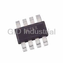
TRANS NPN DUAL LOSAT 50V 832-MLP
Part Number
ZXTDCM832TA
Price
Request Quote
Manufacturer
ZETEX SEMICONDUCTORS
Lead Time
Request Quote
Category
PRODUCTS - Z
Datasheet

Extracted Text
ZXTDCM832 MPPS™ Miniature Package Power Solutions DUAL 50V NPN SILICON LOW SATURATION SWITCHING TRANSISTOR SUMMARY V =50V; R = 68m ;I = 4A CEO SAT C DESCRIPTION Packaged in the innovative 3mm x 2mm MLP (Micro Leaded Package) outline, th these new 4 generation low saturation dual transistors offer extremely low on state losses making them ideal for use in DC-DC circuits and various driving and power management functions. Additionally users gain several other key benefits: Performance capability equivalent to much larger packges Improved circuit efficiency & power levels 3mm x 2mm (Dual die) MLP PCB area and device placement savings Lower package height (nom 0.9mm) C1 C2 Reduced component count FEATURES • Low Equivalent On Resistance B2 B1 • Extremely Low Saturation Voltage (100mV @1A) • h characterised up to 6A FE • I =4A Continuous Collector Current C E2 E1 • 3mm x 2mm MLP APPLICATIONS • DC - DC Converters • Charging circuits • CCFL Backlighting PINOUT • Power switches • Motor control ORDERING INFORMATION DEVICE REEL TAPE QUANTITY WIDTH PER REEL ZXTDCM832TA 7�� 8mm 3000 ZXTDCM832TC 13�� 8mm 10000 3mm x 2mm MLP underside view DEVICE MARKING DCC ISSUE 1 - JUNE 2002 1 ZXTDCM832 ABSOLUTE MAXIMUM RATINGS. PARAMETER SYMBOL LIMIT UNIT Collector-Base Voltage V 100 V CBO Collector-Emitter Voltage V 50 V CEO Emitter-Base Voltage V 7.5 V EBO Peak Pulse Current I 6A CM Continuous Collector Current (a)(f) I 4A C Base Current I 1000 mA B Power Dissipation at TA=25°C (a)(f) P 1.5 W D 12 mW/°C Linear Derating Factor Power Dissipation at TA=25°C (b)(f) P 2.45 W D 19.6 mW/°C Linear Derating Factor Power Dissipation at TA=25°C (c)(f) P 1 W D 8 mW/°C Linear Derating Factor Power Dissipation at TA=25°C (d)(f) P 1.13 W D 9 mW/°C Linear Derating Factor Power Dissipation at TA=25°C (d)(g) P 1.7 W D 13.6 mW/°C Linear Derating Factor Power Dissipation at TA=25°C (e)(g) P 3 W D 24 mW/°C Linear Derating Factor Operating and Storage Temperature Range T :T -55 to +150 °C j stg THERMAL RESISTANCE PARAMETER SYMBOL VALUE UNIT Junction to Ambient (a)(f) R 83.3 °C/W θJA Junction to Ambient (b)(f) R 51 °C/W θJA Junction to Ambient (c)(f) R 125 °C/W θJA Junction to Ambient (d)(f) R 111 °C/W θJA Junction to Ambient (d)(g) R 73.5 °C/W θJA Junction to Ambient (e)(g) R 41.7 °C/W θJA Notes (a) For a dual device surface mounted on 8 sq cm single sided 2oz copper on FR4 PCB, in still air conditions with all exposed pads attached. The copper area is split down the centre line into two separate areas with one half connected to each half of the dual device. (b) Measured at t<5 secs for a dual device surface mounted on 8 sq cm single sided 2oz copper on FR4 PCB, in still air conditions with all exposed pads attached. The copper area is split down the centre line into two separate areas with one half connected to each half of the dual device. (c) For a dual device surface mounted on 8 sq cm single sided 2oz copper on FR4 PCB, in still air conditions with minimal lead connections only. (d) For a dual device surface mounted on 10 sq cm single sided 1oz copper on FR4 PCB, in still air conditions with all exposed pads attached attached. The copper area is split down the centre line into two separate areas with one half connected to each half of the dual device. (e) For a dual device surface mounted on 85 sq cm single sided 2oz copper on FR4 PCB, in still air conditions with all exposed pads attached attached. The copper area is split down the centre line into two separate areas with one half connected to each half of the dual device. (f) For a dual device with one active die. (g) For dual device with 2 active die running at equal power. (h) Repetitive rating - pulse width limited by max junction temperature. Refer to Transient Thermal Impedance graph. (i) The minimum copper dimensions required for mounting are no smaller than the exposed metal pads on the base of the device as shown in the package dimensions data. The thermal resistance for a dual device mounted on 1.5mm thick FR4 board using minimum copper 1 oz weight, 1mm wide tracks and one half of the device active is Rth = 250°C/W giving a power rating of Ptot = 500mW. ISSUE 1 - JUNE 2002 2 ZXTDCM832 TYPICAL CHARACTERISTICS 3.5 V 10 CE(SAT) T =25°C 2oz Cu amb Limited 3.0 Note (e)(g) 2.5 2oz Cu 1 Note (a)(f) DC 2.0 1oz Cu 1s 1.5 Note (d)(g) 100ms 0.1 10ms 1.0 1ms Note (a)(f) 100us 1oz Cu 0.5 0.01 Single Pulse, T =25°C Note (d)(f) amb 0.0 0.1 1 10 100 0 25 50 75 100 125 150 V Collector-Emitter Voltage (V) Temperature (°C) CE Safe Operating Area Derating Curve 225 Note (a)(f) 80 200 1oz copper 175 Note (f) 1oz copper 60 150 Note (g) 125 D=0.5 40 100 75 Single Pulse 2oz copper D=0.2 20 50 Note (f) D=0.05 2oz copper 25 Note (g) D=0.1 0 0 100µ 1m 10m 100m 1 10 100 1k 0.1 1 10 100 Pulse W idth (s) BoardCuArea(sqcm) Transient Thermal Impedance Thermal Resistance v Board Area 3.5 T =25°C 2oz copper amb 3.0 Note (g) T =150°C jmax Continuous 2.5 2oz copper 2.0 Note (f) 1.5 1.0 1oz copper 0.5 1oz copper Note (g) Note (f) 0.0 0.1 1 10 100 BoardCuArea(sqcm) Power Dissipation v Board Area ISSUE 1 - JUNE 2002 3 P Dissipation (W ) I Collector Current (A) D Thermal Resistance (°C/W) C Thermal Resistance (°C/W) Max Power Dissipation (W ) ZXTDCM832 ELECTRICAL CHARACTERISTICS (at T = 25°C unless otherwise stated). amb PARAMETER SYMBOL MIN. TYP. MAX. UNIT CONDITIONS. Collector-Base Breakdown V 100 190 V I =100�A (BR)CBO C Voltage Collector-Emitter Breakdown V 50 65 V I =10mA* (BR)CEO C Voltage Emitter-Base Breakdown Voltage V 7.5 8.2 V I =100�A (BR)EBO E Collector Cut-Off Current I 25 nA V =80V CBO CB Emitter Cut-Off Current I 25 nA V =6V EBO EB Collector Emitter Cut-Off Current I 25 nA V =40V CES CES Collector-Emitter Saturation V 10 20 mV I =0.1A, I =10mA* CE(sat) C B Voltage 70 100 mV I =1A, I =50mA* C B 145 200 mV I =1A, I =10mA* C B 115 220 mV I =2A, I =50mA* C B 225 300 mV I =3A, I =100mA* C B 270 320 mV I =4A, I =200mA* C B Base-Emitter Saturation Voltage V 1.00 1.05 V I =4A, I =200mA* BE(sat) C B Base-Emitter Turn-On Voltage V 0.94 1.00 V I =4A, V =2V* BE(on) C CE Static Forward Current Transfer h 200 400 I =10mA, V =2V* FE C CE Ratio 300 450 I =0.2A, V =2V* C CE 200 400 I =1A, V =2V* C CE 100 225 I =2A, V =2V* C CE 40 I =6A, V =2V* C CE Transition Frequency f 100 165 MHz I =50mA, V =10V T C CE f=100MHz Output Capacitance C 12 20 pF V =10V, f=1MHz obo CB Turn-On Time t 170 ns V =10V, I =1A (on) CC C I =I =10mA Turn-Off Time t 750 ns B1 B2 (off) *Measured under pulsed conditions. Pulse width=300µs. Duty cycle ≤ 2% ISSUE 1 - JUNE 2002 4 ZXTDCM832 TYPICAL CHARACTERISTICS 0.25 Tamb=25°C I /I =50 C B 0.20 100m I /I =100 C B 100°C 0.15 25°C I /I =50 0.10 C B 10m -55°C I /I =10 0.05 C B 1m 0.00 1m 10m 100m 1 10 1m 10m 100m 1 10 I Collector Current (A) I Collector Current (A) C C V vI V vI CE(SAT) C CE(SAT) C 630 1.0 V =2V I /I =50 CE C B 1.2 540 100°C 1.0 450 0.8 -55°C 25°C 0.8 360 0.6 270 0.6 25°C -55°C 0.4 180 100°C 0.2 90 0.4 0.0 0 1m 10m 100m 1 10 1m 10m 100m 1 10 I Collector Current (A) I Collector Current (A) C C h vI V vI FE C BE(SAT) C 1.0 V =2V CE 0.8 -55°C 0.6 25°C 100°C 0.4 1m 10m 100m 1 10 I Collector Current (A) C V vI BE(ON) C ISSUE 1 - JUNE 2002 5 V (V) Normalised Gain V (V) BE(ON) CE(SAT) Typical Gain (h ) FE V (V) V (V) BE(SAT) CE(SAT) ZXTDCM832 MLP832 PACKAGE OUTLINE (3mm x 2mm Micro Leaded Package) CONTROLLING DIMENSIONS IN MILLIMETRES APPROX. CONVERTED DIMENSIONS IN INCHES MLP832 PACKAGE DIMENSIONS MILLIMETRES INCHES MILLIMETRES INCHES DIM DIM MIN. MAX. MIN. MAX. MIN. MAX. MIN. MAX. A 0.80 1.00 0.031 0.039 e 0.65 REF 0.0256 BSC A1 0.00 0.05 0.00 0.002 E 2.00 BSC 0.0787 BSC A2 0.65 0.75 0.0255 0.0295 E2 0.43 0.63 0.017 0.0249 A3 0.15 0.25 0.006 0.0098 E4 0.16 0.36 0.006 0.014 b 0.24 0.34 0.009 0.013 L 0.20 0.45 0.0078 0.0157 b1 0.17 0.30 0.0066 0.0118 L2 0.125 0.00 0.005 D 3.00 BSC 0.118 BSC r 0.075 BSC 0.0029 BSC D2 0.82 1.02 0.032 0.040 � 0� 12� 0� 12� D3 1.01 1.21 0.0397 0.0476 © Zetex plc 2002 Europe Americas Asia Pacific Zetex plc Zetex GmbH Zetex Inc Zetex (Asia) Ltd Fields New Road Streitfeldstraße 19 700 Veterans Memorial Hwy 3701-04 Metroplaza, Tower 1 Chadderton D-81673 München Hauppauge, NY11788 Hing Fong Road Oldham, OL9 8NP Kwai Fong United Kingdom Germany USA Hong Kong Telephone (44) 161 622 4422 Telefon: (49) 89 45 49 49 0 Telephone: (631) 360 2222 Telephone: (852) 26100 611 Fax: (44) 161 622 4420 Fax: (49) 89 45 49 49 49 Fax: (631) 360 8222 Fax: (852) 24250 494 uksales@zetex.com europe.sales@zetex.com usa.sales@zetex.com asia.sales@zetex.com These offices are supported by agents and distributors in major countries world-wide. This publication is issued to provide outline information only which (unless agreed by the Company in writing) may not be used, applied or reproduced for any purpose or form part of any order or contract or be regarded as a representation relating to the products or services concerned. The Company reserves the right to alter without notice the specification, design, price or conditions of supply of any product or service. For the latest product information, log on to www.zetex.com ISSUE 1 - JUNE 2002 6
Frequently asked questions
What makes Elite.Parts unique?

What kind of warranty will the ZXTDCM832TA have?
Which carriers does Elite.Parts work with?
Will Elite.Parts sell to me even though I live outside the USA?
I have a preferred payment method. Will Elite.Parts accept it?


What they say about us
FANTASTIC RESOURCE
One of our top priorities is maintaining our business with precision, and we are constantly looking for affiliates that can help us achieve our goal. With the aid of GID Industrial, our obsolete product management has never been more efficient. They have been a great resource to our company, and have quickly become a go-to supplier on our list!
Bucher Emhart Glass
EXCELLENT SERVICE
With our strict fundamentals and high expectations, we were surprised when we came across GID Industrial and their competitive pricing. When we approached them with our issue, they were incredibly confident in being able to provide us with a seamless solution at the best price for us. GID Industrial quickly understood our needs and provided us with excellent service, as well as fully tested product to ensure what we received would be the right fit for our company.
Fuji
HARD TO FIND A BETTER PROVIDER
Our company provides services to aid in the manufacture of technological products, such as semiconductors and flat panel displays, and often searching for distributors of obsolete product we require can waste time and money. Finding GID Industrial proved to be a great asset to our company, with cost effective solutions and superior knowledge on all of their materials, it’d be hard to find a better provider of obsolete or hard to find products.
Applied Materials
CONSISTENTLY DELIVERS QUALITY SOLUTIONS
Over the years, the equipment used in our company becomes discontinued, but they’re still of great use to us and our customers. Once these products are no longer available through the manufacturer, finding a reliable, quick supplier is a necessity, and luckily for us, GID Industrial has provided the most trustworthy, quality solutions to our obsolete component needs.
Nidec Vamco
TERRIFIC RESOURCE
This company has been a terrific help to us (I work for Trican Well Service) in sourcing the Micron Ram Memory we needed for our Siemens computers. Great service! And great pricing! I know when the product is shipping and when it will arrive, all the way through the ordering process.
Trican Well Service
GO TO SOURCE
When I can't find an obsolete part, I first call GID and they'll come up with my parts every time. Great customer service and follow up as well. Scott emails me from time to time to touch base and see if we're having trouble finding something.....which is often with our 25 yr old equipment.
ConAgra Foods