

 Manufacturers
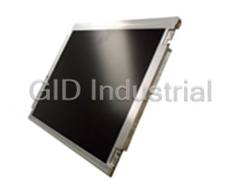
VERTEX LCD LVM104XSB-01
Description
10.4" Sunlight Readable 1200 nits TFT LCD XGA
Part Number
LVM104XSB-01
Price
Request Quote
Manufacturer
VERTEX LCD
Lead Time
Request Quote
Category
PRODUCTS - L
Datasheet

Extracted Text
TENTATIVE PRODUCT INFORMATION
(All information in this technical data sheet is tentative and
subject to change without notice.)
Updated: 12/31/2003
10.4” XGA Very High Bright TFT-LCD
LVM104XSB-01
(based on HYDIS:HT10X21)
COLOR LIQUID CRYSTAL DISPLAY
Vertex LCD Inc. (1/21) LVM104XSB-01Rev. 2.0
CONTENTS
NO. ITEM Page
- COVER 1
- CONTENTS 2
- REVISION HISTORY 3
1 GENERAL DESCRIPTION 4
2 ABSOLUTE MAXIMUM RATINGS 4
3 ELECTRICAL CHARACTERISTICS 5
4 POWER ON/OFF SEQUENCE 6
5 INTERFACE CONNECTION 7
5D RECOMMENDED LVDS TRANSMITTER 8, 9
6 SIGNAL TIMING SPECIFICATIONS 10
7 TIMING WAVE FORM 11
8 COLOR INPUT DATA REFERENCE 12
9 BLOCK DIAGRAM 13
10 OPTICAL SPECIFICATIONS 14
11 MECHANICAL CHARACTERISTICS 15
12 MECHANICAL SPECIFICATIONS 16, 17
13 RELIABILITY 18
14 PACKING FORM 18
15 PRECAUTIONS 18
15-1 MOUNTING PRECAUTION 18, 19
15-2 OPERATING PRECAUTION 19
15-3 ELECTROSTATIC DISCHARGE CONTROL 19
15-4 STORAGE 19
15-5 HANDLING PRECAUTION FOR PROTECTION FILM 19, 20
A OPTICAL CHARACTERISTIC MEASUREMENT EQUIPMENT AND METHOD 20
B LUMINANCE 20
C RESPONSE TIME 21
D VIEWING ANGLE 21
Vertex LCD Inc. (2/21) LVM104XSB-01Rev. 2.0
Revision History
Rev ECN No. Description of changes Date Prepared
0 Preliminary 6/5/03 Gene Huh
1 All Changed 9/24/03 Eric Kim
2 Outline Dimensions 12/31/03 Eric Kim
238.1(H)×177.4(V)×11.0(D) mm
Æ238.5(H)×177.8(V)×11.2(D) mm
Bezel Opening Dimensions
216.60 Æ 214.40, 162.40 Æ 161.80
Outline Drawing
Vertex LCD Inc. (3/21) LVM104XSB-01Rev. 2.0
1. General Description
LVM104XSB-01 is 10.4” Color Active Matrix Liquid Crystal Display with an integral Cold Cathode Fluorescent Lamp
(CCFL) backlight system. The matrix employs amorphous silicon Thin Film Transistor as the active element. It is a
transmissive type display operating in the normally black mode. This TFT-LCD has a 10.4 inch diagonally measured
active display area with XGA resolution (768 horizontal by 1024 vertical pixel array). Each pixel is divided into Red,
Green and Blue sub-pixels or dots which are arranged in vertical stripes. Gray scale or the brightness of the sub-pixel
color is determined with a 6-bit gray scale signal for each dot, thus presenting a palette of more than 262,144 colors.
The LVM104XSB-01 is intended to support applications where high brightness is a critical factor. In combination with
the vertical arrangement of the sub-pixels, the LVM104XSB-01 characteristics provide an excellent flat panel display
for office or industrial automation products or daylight applications.
General Specification
General specifications are summarized in the following table:
ITEM SPECIFICATION
Active screen size 10.4 inches(26cm) diagonal
210.432(H) X 157.824(V) mm
Outline dimensions 238.5(H) × 177.8(V) × 11.2(D) mm
Pixel pitch 0.2055(H) mm × 0.2055(V) mm
Pixel format 1024(H) X 768(V) pixels
Color Pixel Arrangement RGB stripe arrangement
Color depth 6-bit, 262,144 colors
2
Brightness 1,200 cd/m
Power Consumption (LCD Total 21.8 Watt,typ (0.7Watt @Vcc, 21.1
& Backlight only) Watt @Lamp)
Weight 600g (typ)
Display operating mode transmissive mode, normally Black
Surface treatments hard coating(3H), anti-glare, Haze 25
Backlight Unit CCFL, 4 tubes
2. Absolute Maximum Rating
Values
Parameter symbol Units Notes
Min. Max.
o
Power Input Voltage VCC -0.3 +4.0 Vdc at 25 C
o
Operating Temperature T 0 +50 C 1
OP
(with the heater)
o
C
Storage Temperature TST -20 +60 1
Note: Humidity ≤ 90% RH. No condensation.
Vertex LCD Inc. (4/21) LVM104XSB-01Rev. 2.0
3. Electrical Characteristics
The LVM104XSB-01 requires three power inputs. One is employed to power the LCD electronics and to drive the TFT
array and liquid crystal. The second input which powers the CCFL, is typically generated by an inverter. The inverter
is an external unit to the LCD.
Parameter Symbol Values Units Notes
Min. Typ. Max.
MODULE:
Power Supply Input Voltage VCC 3.0 3.3 3.6 Vdc Vcc = 3.3 V
Power Supply Input Current I - 0.210 - A 1 Vcc = 3.3 V
CC
Power Consumption Pc - 0.7 - Watts
LAMP:
Operating Voltage VBL 960 VRMS
Operating Current I 5.5 6.0 mA 3
BL
Established Starting Voltage
o
at 25 C 1100 1320 VRMS 4
o
at 0 C - 1280 1590 VRMS
Operating Frequency f 40 55 60 kHz 5
BL
Power Consumption P 21.1 Watts 6
BL
Life Time 10,000 40,000 Hrs 7
o
Notes: 1. The current draw and power consumption specified is for 3.3 Vdc at 25 C and fv at 60Hz.(at Black
pattern displayed)
o
2. Logic level are specified for Vcc of 3.3 Vdc at 25 C. The values specified apply to all logic inputs; Hsync, Vsync,
Clock, data signals, etc.
±
3. The variance of the voltage is 10%.
4. The output voltage at the transformer in the inverter must be high considering to the loss of the
ballast capacitor in the inverter.
5. Lamp frequency may produce interference with horizontal sync. frequency and may cause beat on the
display. Therefore lamp frequency shall be detached as much as from the horizontal sync. and from the
harmonics of horizontal synchronous to avoid interference.
6. The lamp power consumption shown above does not include loss of external inverter.
7. The life time is determined as the time at which brightness of lamp is 50% compare to that of initial
value at the typical lamp current.
Vertex LCD Inc. (5/21) LVM104XSB-01Rev. 2.0
4. Power On/Off Sequences
To prevent a latch-up or DC operation of the LCD module, the power on/off sequence should be as shown below.
0.9VDD 0.9VDD
Power Supply
0.1VDD
0.1VDD
0V
T1
T5
T2 T6
Valid
Interface Signal
0
T3 T4
Back- light
0
• 0 < T1 ≤ 10 ms
• 0 < T2 ≤ 50 ms
• 100 ms ≤ T3, T4
• 0 < T5 ≤ 50 ms
• 1 sec < T6
Note: 1. Please avoid floating state of interface signal at invalid period.
2. When the interface signal is invalid, be sure to pull down the power supply for LCD Vcc to
0 Vcd.
3. Lamp power must be turn on after power supply for LCD and interface signal is valid.
Vertex LCD Inc. (6/21) LVM104XSB-01Rev. 2.0
5. Interface Connections
CN 1(interface signal): LVM104XSB-01 uses 14 pin connector for module electronics.
Used connector: DF19L-14P-1H (HIROSE Electric Co. LTD) Matching side: DF19G-14S-1C (HIROSE)
Pin Symbol Description
1 V Power supply +3.3V
DD
2 VDD Power supply +3.3V
3 Vss Ground
4 Vss Ground
5 RIN0- Transmission Data of Pixel 0 (-)
6 RIN0+ Transmission Data of Pixel 0 (+)
7 RIN1- Transmission Data of Pixel 1 (-)
8 RIN1+ Transmission Data of Pixel 1 (+)
9 RIN2- Transmission Data of Pixel 2 (-)
10 RIN2+ Transmission Data of Pixel 2 (+)
11 RCLK IN- Sampling Clock (-)
12 RCLK IN+ Sampling Clock (+)
13 VSS Ground
14 VSS Ground
CN 2(backlight): LVM104XSB-01 employs BHR-02VS-1 manufactured by JST.
Pin Symbol Description Notes
1 HV Lamp power input PINK
2 LV Ground WHITE
Notes : 1. The input power terminal is colored pink (or gray). Ground pin color is white.
2. The lamp ground should be common with GND.
Vertex LCD Inc. (7/21) LVM104XSB-01Rev. 2.0
5.1. Recommended Transmitter to LVM104XSB-01
6 Bit Transmitter (THC63LVDM63A)
THC63LVDM63A LVM104XSB-01
Interface
Input Terminal No. Input Signal
(CN1)
(Graphic controller output signal) Output Signal
Symbol
Symbol THC63LVDM63A Symbol Function Terminal Symbol
TIN0 44 R0 Red Pixels Display Data (LSB)
TIN1 45 R1 Red Pixels Display Data
TIN2 47 R2 Red Pixels Display Data
OUT0 -
No. 5 IN0 –
TIN3 48 R3 Red Pixels Display Data
OUT0+
No. 6 IN0 +
TIN4 1 R4 Red Pixels Display Data
TIN5 3 R5 Red Pixels Display Data (MSB)
TIN6 4 G0 Green Pixels Display Data (LSB)
TIN7 6 G1 Green Pixels Display Data
TIN8 7 G2 Green Pixels Display Data
TIN9 9 G3 Green Pixels Display Data
OUT1 – No. 7 IN1 –
TIN10 10 G4 Green Pixels Display Data
OUT1 + No. 8 IN1 +
TIN11 12 G5 Green Pixels Display Data (MSB)
TIN12 13 B0 Blue Pixels Display Data (LSB)
TIN13 15 B1 Blue Pixels Display Data
TIN14 16 B2 Blue Pixels Display Data
TIN15 18 B3 Blue Pixels Display Data
TIN16 19 B4 Blue Pixels Display Data
OUT2 – No. 9 IN2 –
TIN17 20 B5 Blue Pixels Display Data (MSB)
OUT2 + No. 10 IN2 +
TIN18 22 Hsync Horizontal Synchronization Signal
TIN19 23 Vsync Vertical Synchronization Signal
TIN20 25 DE Compound Synchronization Signal
CLK IN 26 NCLK Data Sampling Clock CLK OUT – No. 11 CLK IN –
CLK OUT + No. 12 CLK IN +
Vertex LCD Inc. (8/21) LVM104XSB-01Rev. 2.0
8 Bit Transmitter (THC63LVDM83A)
THC63LVDM83A LVM104XSB-01
Input Terminal No. Input Signal Output Signal Interface
(Graphic controller output signal) Symbol (CN1)
Symbol THC63LVDM83 Symbol Function Terminal Symbol
TIN0 51 R0 Red Pixels Display Data (LSB)
TIN1 52 R1 Red Pixels Display Data
OUT0 –
No. 5 IN0 –
TIN2 54 R2 Red Pixels Display Data
OUT0 +
No. 6 IN0 +
TIN3 55 R3 Red Pixels Display Data
TIN4 56 R4 Red Pixels Display Data
TIN6 3 R5 Red Pixels Display Data (MSB)
TIN7 4 G0 Green Pixels Display Data (LSB)
TIN8 6 G1 Green Pixels Display Data
TIN9 7 G2 Green Pixels Display Data
OUT1 – No. 7 IN1 –
TIN12 11 G3 Green Pixels Display Data
OUT1 + No. 8 IN1 +
TIN13 12 G4 Green Pixels Display Data
TIN14 14 G5 Green Pixels Display Data (MSB)
TIN15 15 B0 Blue Pixels Display Data (LSB)
TIN18 19 B1 Blue Pixels Display Data
TIN19 20 B2 Blue Pixels Display Data
TIN20 22 B3 Blue Pixels Display Data
OUT2 – No. 9 IN2 –
TIN21 23 B4 Blue Pixels Display Data
OUT2 + No. 10 IN2 +
TIN22 24 B5 Blue Pixels Display Data (MSB)
TIN24 27 Hsync Horizontal Synchronization Signal
TIN25 28 Vsync Vertical Synchronization Signal
TIN26 30 DE Compound Synchronization Signal
TIN27 50 NC Non Connection (open)
TIN5 2 NC Non Connection (open)
OUT3 –
TIN10 8 NC Non Connection (open)
OUT3 +
TIN11 10 NC Non Connection (open)
TIN16 16 NC Non Connection (open)
TIN17 18 NC Non Connection (open)
TIN23 25 NC Non Connection (open)
CLK IN 31 NCLK Data Sampling Clock CLK OUT – No. 11 CLK IN –
CLK OUT + No. 12 CLK IN +
Vertex LCD Inc. (9/21) LVM104XSB-01Rev. 2.0
6. Signal Timing Specification
The 10.4XGA LCM is only operated by the DE mode
Item Symbols Min Typ Max Units
Frequency 1/Tc - 65 80 MHz
Clock
High Time Tch 4.5 - - Ns
Low Time Tcl 4.5 - - Ns
Data Setup Time Tds 2.7 - - Ns
Hold Time Tdh 0 - - Ns
Data Enable Setup Time Tes 2.7 - - Ns
Frame Period Tv 772 806 1022 Lines
Vertical Display Period Tvd 768 768 768 Lines
One Line Scanning Period Th 1100 1344 2046 Clocks
Horizontal Display Period Thd 1024 1024 1024 Clocks
Note 1) Refer to TIMING CHART and LVDS (THC63LVDF64A) specifications by Thine Electronics Inc.
Note 2) If NCLK is fixed to “H” or “L” level for certain period, the panel may be damaged.
Note 3) Please adjust LCD operating signal timing and FL driving frequency, to optimize the display
quality.
note 4) Do not hold NCLK on “H” level nor “L” level during VDD (+3.3V) is supplied. When it holds on,
DC voltage supplies to liquid crystal materials and it may cause damage to liquid crystal materials.
note 5) Do not make tv, tvhd and tvds fluctuate.
If tv, tvhd and tvds are fluctuated, then panel displays black.
note 6) NCLK count of each Horizontal Scanning Time should be always the same.
V-Blanking period should be “n” X “Horizontal Scanning Time”. (n: integer)
-LVDS Rx interface timing parameter
Item Symbol Min Typ. Max Unit Remark
CLKIN Period RCIP 12.5 15.38 - nsec
t
Input data 0 RIP1 -0.4 0.0 +0.4 nsec
t
Input data 1 RIP0 1 * RIPC/7-0.4 1 * RIPC/7 1 * RIPC/7+0.4 nsec
t t t t
Input data 2 RIP6 2 * RIPC/7-0.4 2 * RIPC/7 2 * RIPC/7+0.4 nsec
t t t t
Input data 3 tRIP5 3 * tRIPC/7-0.4 3 * tRIPC/7 3 * tRIPC/7+0.4 nsec
Input data 4 tRIP4 4 * tRIPC/7-0.4 4 * tRIPC/7 4 * tRIPC/7+0.4 nsec
Input data 5 tRIP3 5 * tRIPC/7-0.4 5 * tRIPC/7 5 * tRIPC/7+0.4 nsec
Input data 6 tRIP2 6 * tRIPC/7-0.4 6 * tRIPC/7 6 * tRIPC/7+0.4 nsec
RIP2
t
tRIP3
RIP4
t
tRIP5
tRIP6
RIP0
t
tRIP1
Rx3 Rx2 Rx1 Rx0 Rx6 Rx5 Rx4 Rx3 Rx2 Rx1 Rx0
RINz +/-
Vdiff=0[v] Vdiff=0[v]
RCLKIN+
tRCIP
* Z=0, 1, 2, 3
* Vdiff = (RINz+)-(RINz-), (RCLKIN+)-(RCLKIN-)
Vertex LCD Inc. (10/21) LVM104XSB-01Rev. 2.0
7. Timing Wave Form(DE Mode)
Vertical Timing Waveforms
Tv
Tvd
MCLK
Th
ENAB
R7 ~ R0
G7 ~ G0 Invalid Data x,1 x,2 x,y x,768 Invalid Data x+1,1
B7 ~ B0
Horizontal Timing Waveforms
Th
Thd
MCLK
Tc
ENAB
RA7 ~RA0
GA7 ~GA0
D1022 D1023 D1024
D1 D2 Dn Invalid Data D1 D2 D3
BA7 ~BA0
Tch
Tcl
2.0V
1.5V
MCLK
0.8V
Tds
Tdh
2.0V
Data
V a lid Data
0.8V
Tes
ENAB 2.0V
Vertex LCD Inc. (11/21) LVM104XSB-01Rev. 2.0
8. Color Input Data Reference
The brightness of each primary color(red, green and blue) is based on the 6-bit gray scale data input for the color;
the higher the binary input, the brighter the color. The table below provides a reference for color versus data input.
R5 R4 R3 R2 R1 R0 G5 G4 G3 G2 G1 G0 B5 B4 B3 B2 B1 B0
Display
Black 0 0 0 0 0 0 0 0 0 0 0 0 0 0 0 0 0 0
Blue 0 0 0 0 0 0 0 0 0 0 0 0 1 1 1 1 1 1
Green 0 0 0 0 0 0 1 1 1 1 1 1 0 0 0 0 0 0
Basic Light Blue 0 0 0 0 0 0 1 1 1 1 1 1 1 1 1 1 1 1
Colors Red 1 1 1 1 1 1 0 0 0 0 0 0 0 0 0 0 0 0
Purple 1 1 1 1 1 1 0 0 0 0 0 0 1 1 1 1 1 1
Yellow 1 1 1 1 1 1 1 1 1 1 1 1 0 0 0 0 0 0
White 1 1 1 1 1 1 1 1 1 1 1 1 1 1 1 1 1 1
Red(00) Dark 0 0 0 0 0 0 0 0 0 0 0 0 0 0 0 0 0 0
Red(01) 0 0 0 0 0 1 0 0 0 0 0 0 0 0 0 0 0 0
Red(02) 0 0 0 0 1 0 0 0 0 0 0 0 0 0 0 0 0 0
Red : : : : : : : : : : : : : : : : : :
Red(61) 1 1 1 1 0 1 0 0 0 0 0 0 0 0 0 0 0 0
Red(62) 1 1 1 1 1 0 0 0 0 0 0 0 0 0 0 0 0 0
Red(63) Bright 1 1 1 1 1 1 0 0 0 0 0 0 0 0 0 0 0 0
Green(00)Dark 0 0 0 0 0 0 0 0 0 0 0 0 0 0 0 0 0 0
Green(01) 0 0 0 0 0
0 0 0 0 0 0 1 0 0 0 0 0 0
Green(02) 0 0 0 0 0 0 0 0 0 0 1 0 0 0 0 0 0 0
Green : : : : : : : : : : : : : : : : : :
Green(61) 0 0 0 0 0 0 1 1 1 1 0 1 0 0 0 0 0 0
Green(62) 0 0 0 0 0 0 1 1 1 1 1 0 0 0 0 0 0 0
Green(63)Bright 0 0 0 0 0 0 1 1 1 1 1 1 0 0 0 0 0 0
Blue(00) Dark 0 0 0 0 0 0 0 0 0 0 0 0 0 0 0 0 0 0
Blue(01) 0 0 0 0 0 0 0 0 0 0 0 0 0 0 0 0 0 1
Blue(02) 0 0 0 0 0 0 0 0 0 0 0 0 0 0 0 0 1 0
Blue : : : : : : : : : : : : : : : : : :
Blue(61) 0 0 0 0 0 0 0 0 0 0 0 0 1 1 1 1 0 1
Blue(62) 0 0 0 0 0 0 0 0 0 0 0 0 1 1 1 1 1 0
Blue(63) Bright 0 0 0 0 0 0 0 0 0 0 0 0 1 1 1 1 1 1
Black(00) Dark 0 0 0 0 0 0 0 0 0 0 0 0 0 0 0 0 0 0
(01) 0 0 0 0 0 1 0 0 0 0 0 1 0 0 0 0 0 1
Whte & (02) 0 0 0 0 1 0 0 0 0 0 1 0 0 0 0 0 1 0
Black : : : : : : : : : : : : : : : : : :
(61)
1 1 1 1 0 1 1 1 1 1 0 1 1 1 1 1 0 1
(62) 1 1 1 1 1 0 1 1 1 1 1 0 1 1 1 1 1 0
White(63) Bright 1 1 1 1 1 1 1 1 1 1 1 1 1 1 1 1 1 1
Vertex LCD Inc. (12/21) LVM104XSB-01Rev. 2.0
9. Block Diagram
Panel
Column driver circuit
Controller
+ LVDS
DC/DC
TFT-LCD
Converter
(1024×768)
Gray scale
Manipulation
Voltage
Generation
Circuit
D/A
Converter
Circuit
CN2 Backlight Ass’y(4CCFL)
Vertex LCD Inc. (13/21) LVM104XSB-01Rev. 2.0
CN1
Row Driver circuit
10. Optical Specifications
Optical characteristics are determined after the unit has been ‘ON’ and stable for approximately 30 minutes in a
o
dark environment at 25 C. The values specified are at an approximate distance 50cm from the LCD surface at a
viewing angle of Φ and θ equal to 0°.
Appendix A presents additional information concerning the measurement equipment and method.
Parameter Symbol Values Units Notes
Min. Typ. Max.
Contrast Ratio CR - 450 - 1
2
Surface Luminance, white L 1000 1200 cd/m 2
WH
δ WHITE
Luminance Uniformity 70% 3
Response Time
Total(Tr + Td) 34 40 msec 4
CIE Color Coordinates -
Red x - 0.543 -
R
yR - 0.334 -
Green xG - 0.317 -
y - 0.500 -
G
Blue xB - 0.156 -
yB - 0.151 -
White x - 0.312 -
W
yW 0.343
Viewing Angle
x axis, right (∅=0º) θ x - 80 - degree 5
x axis, left(∅=180º) θ x - 80 -
θ
y axis, up(∅=90º) y - 80 -
y axis, down (∅=270º) θ y - 80 -
Notes 1. Contrast Ratio (CR) is defined mathematically as :
Surface Luminance with all white pixels
Contrast Ratio =
Surface Luminance with all black pixels
2. Surface luminance is the center point across the LCD surface 50cm from the surface with all pixels
displaying white. For more information see Appendix B.
3. The uniformity in surface Luminance, δ WHITE is determined by measuring LON at each test position 1 through
9, and then dividing the minimum LON of 9 points luminance by maximum LON of 9 points luminance and
multiply by 100 for percentage value. For more information see Appendix B.
δ WHITE = Minimum (LON1, LON2, ....LON9) * 100 / Maximum (LON1, LON2, ....LON9)
4. Response time is the time required for the display to transition from white to black (Rise Time, Tr ) and from
R
black to white (Decay Time, Tr ). For additional information see Appendix C.
D
5. Viewing angle is the angle at which the contrast ratio is greater than 10. The angles are determined for the
horizontal or x-axis and the vertical or y-axis with respect to the z-axis which is normal to the LCD surface. For
more information see Appendix D.
Vertex LCD Inc. (14/21) LVM104XSB-01Rev. 2.0
11. Mechanical Characteristics
The chart below provides general mechanical characteristics for the model LVM104XSB-01. In addition, the figure
below is a detailed mechanical drawing of the LCD. Note that dimensions are given for reference purposes only.
Outside dimensions:
Horizontal 238.50 ± 0.5 mm
Vertical 177.80 ± 0.5 mm
Depth 11.20 ± 0.3 mm
Bezel area:
Horizontal 214.40 mm
Vertical 161.80 mm
Active Display area:
Horizontal 210.432 mm
Vertical 157.824 mm
Weight (approximate): 600 g
Surface Treatment: Hard coating 3H.
Anti-glare treatment of the front polarizer.
Vertex LCD Inc. (15/21) LVM104XSB-01Rev. 2.0
12. Mechanical Specification
< FRONT VIEW >
Vertex LCD Inc. (16/21) LVM104XSB-01Rev. 2.0
Frequently asked questions
What makes Elite.Parts unique?

What kind of warranty will the LVM104XSB-01 have?
Which carriers does Elite.Parts work with?
Will Elite.Parts sell to me even though I live outside the USA?
I have a preferred payment method. Will Elite.Parts accept it?


What they say about us
FANTASTIC RESOURCE
One of our top priorities is maintaining our business with precision, and we are constantly looking for affiliates that can help us achieve our goal. With the aid of GID Industrial, our obsolete product management has never been more efficient. They have been a great resource to our company, and have quickly become a go-to supplier on our list!
Bucher Emhart Glass
EXCELLENT SERVICE
With our strict fundamentals and high expectations, we were surprised when we came across GID Industrial and their competitive pricing. When we approached them with our issue, they were incredibly confident in being able to provide us with a seamless solution at the best price for us. GID Industrial quickly understood our needs and provided us with excellent service, as well as fully tested product to ensure what we received would be the right fit for our company.
Fuji
HARD TO FIND A BETTER PROVIDER
Our company provides services to aid in the manufacture of technological products, such as semiconductors and flat panel displays, and often searching for distributors of obsolete product we require can waste time and money. Finding GID Industrial proved to be a great asset to our company, with cost effective solutions and superior knowledge on all of their materials, it’d be hard to find a better provider of obsolete or hard to find products.
Applied Materials
CONSISTENTLY DELIVERS QUALITY SOLUTIONS
Over the years, the equipment used in our company becomes discontinued, but they’re still of great use to us and our customers. Once these products are no longer available through the manufacturer, finding a reliable, quick supplier is a necessity, and luckily for us, GID Industrial has provided the most trustworthy, quality solutions to our obsolete component needs.
Nidec Vamco
TERRIFIC RESOURCE
This company has been a terrific help to us (I work for Trican Well Service) in sourcing the Micron Ram Memory we needed for our Siemens computers. Great service! And great pricing! I know when the product is shipping and when it will arrive, all the way through the ordering process.
Trican Well Service
GO TO SOURCE
When I can't find an obsolete part, I first call GID and they'll come up with my parts every time. Great customer service and follow up as well. Scott emails me from time to time to touch base and see if we're having trouble finding something.....which is often with our 25 yr old equipment.
ConAgra Foods