

 Manufacturers
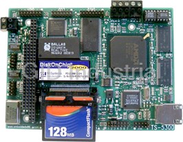
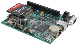
TECHNOLOGIC SYSTEMS TS-5300
Description
Technologic Systems TS-5300 CPU Board with AMD 133 MHz 5x86 Single Board Computer, 2 COM ports, Ethernet, Compact Flash, DIO
Part Number
TS-5300
Price
Request Quote
Manufacturer
TECHNOLOGIC SYSTEMS
Lead Time
Request Quote
Category
PC/104 & PC/104-PLUS
Specifications
Dimensions
4.0" x 5.4" (PC/104 mounting holes)
Ethernet
10 Mbit Ethernet interface - LED indicators
Expansion
PC/104 8/16 bit bus
Flash
2 MB Flash disk with full BIOS support. Compact Flash Card interfaced as IDE0
General
Alphanumeric LCD interface
Matrix Keypad interface on DIO2
Rugged quick-release terminal strips used for power
I/O
40 DIO lines (IRQ capable)
Operating Temperature Range
Fanless -20° to +70°C
Optional Extended Temperature Range
-40° to +80°C
Optional RS-485 support
on COM1 (full or half duplex)
Power requirements
5V DC @ 800 mA
Processor
AMD Elan 520 @ 133 MHz
RTC
On-board Real Time Clock
System Memory
16 MB of High Speed SDRAM (64 MB RAM optional)
Features
- 1 10Mbps Ethernet
- 1 Compact Flash socket
- 16MB SDRAM (64MB opt)
- 2 COM ports
- 2MB Flash (4MB opt)
- 40 DIO
- Dimensions 4.0 x 5.4 inches
- Fanless -20° to +70°C
- Matrix Keypad and text LCD support
- On-board RTC
- Optional Extended Temp. Range
- Optional RS-485 Full/Half Duplex
- PC-Compatible 133MHz 586 CPU
- PC/104 8/16 bit bus
- Power 800mA @ 5V DC
- Watchdog timer
Datasheet

Extracted Text
TS-5300 User’s Manual
Technologic Systems, Incorporated
16525 East Laser Drive
Fountain Hills, AZ 85268
480-837-5200
FAX 837-5300
info@embeddedx86.com
http://www.embeddedx86.com/
This revision of the manual is dated
May 21, 2009
All modifications from previous versions are listed in the appendix.
Copyright © 1998-2008 by Technologic Systems, Inc. All rights reserved.
TS-5300 User’s Manual Technologic Systems
Limited Warranty
Technologic Systems warrants this product to be free of defects in material and workmanship for a
period of one year from date of purchase. During this warranty period Technologic Systems will repair or
replace the defective unit in accordance with the following instructions:
· Contact Technologic Systems and obtain a Return Material Authorization (RMA) number and a copy
of the RMA form.
· Fill out the RMA form completely and include it and dated proof of purchase with the defective unit
being returned. Clearly print the RMA number on the outside of the package.
This limited warranty does not cover damages resulting from lighting or other power surges, misuse,
abuse, abnormal conditions of operation, or attempts to alter or modify the function of the product.
This warranty is limited to the repair or replacement of the defective unit. In no event shall
Technologic Systems be liable or responsible for any loss or damages, including but not limited
to any lost profits, incidental or consequential damages, loss of business, or anticipatory profits
arising from the use or inability to use this product.
Repairs made after the expiration of the warranty period are subject to a flat rate repair charge and the
cost of return shipping. Please contact Technologic Systems to arrange for any repair service.
ii 05/21/09
TS-5300 User’s Manual Technologic Systems
Table Of Contents
LIMITED WARRANTY.......................................................................................................................................................................................II
1 INTRODUCTION ...................................................................................................................................................................................5
2 PC COMPATIBILITY..............................................................................................................................................................................5
2.1 Operating Systems..........................................................................................................................................................................5
3 POWER...................................................................................................................................................................................................6
4 MEMORY.................................................................................................................................................................................................6
4.1 SDRAM...............................................................................................................................................................................................6
4.2 Flash ..................................................................................................................................................................................................6
4.3 Compact Flash cards and DiskOnChip modules.....................................................................................................................6
4.4 Using the SanDisk USB Compact Flash Card Reader .........................................................................................7
4.5 Battery-Backed SRAM ............................................................................................................................................................7
5 SERIAL PORTS .....................................................................................................................................................................................7
5.1 Serial Port Configuration Registers.............................................................................................................................................8
5.2 Serial Port Hardware.......................................................................................................................................................................8
5.3 RS-485 Support ...............................................................................................................................................................................8
5.4 Automatic RS-485 TX Enable........................................................................................................................................................9
5.5 Adding Serial Ports..........................................................................................................................................................................9
6 DIGITAL I/O...........................................................................................................................................................................................10
6.1 DIO1 Header...................................................................................................................................................................................10
6.2 DIO2 Header...................................................................................................................................................................................10
6.3 Using LCD Port as Digital I/O......................................................................................................................................................11
6.4 DIO on the PC/104 bus.................................................................................................................................................................11
7 LCD INTERFACE ................................................................................................................................................................................11
8 MATRIX KEYPAD SUPPORT.............................................................................................................................................................12
9 THE 10 BASE-T ETHERNET PORT.................................................................................................................................................13
10 REAL TIME CLOCK.............................................................................................................................................................................16
11 WATCHDOG TIMER............................................................................................................................................................................17
12 LED AND JUMPERS...........................................................................................................................................................................18
13 PC/104 BUS EXPANSION .................................................................................................................................................................20
14 LOADING OR TRANSFERRING FILES...........................................................................................................................................21
14.1 Developing with the Technologic Systems TS-9500..............................................................................................................21
14.2 Transferring files with Compact Flash......................................................................................................................................21
14.3 Zmodem Downloads ....................................................................................................................................................................21
15 DEBUGGING........................................................................................................................................................................................22
15.1 Integrated BIOS Debugger...........................................................................................................................................................22
15.2 Using other debuggers ................................................................................................................................................................22
16 VIDEO, KEYBOARD, AND CONSOLE REDIRECTION.................................................................................................................23
17 SYSTEM BIOS SETUP SCREENS...................................................................................................................................................24
17.1 Main CMOS Configuration Screen..............................................................................................................................................24
17.2 Basic CMOS Configuration..........................................................................................................................................................25
17.3 Adding a TS-9400 or TS-9500 with Compact Flash...............................................................................................................25
17.4 Custom CMOS Configuration......................................................................................................................................................27
17.5 Shadow Configuration..................................................................................................................................................................28
18 FEEDBACK AND UPDATES TO THE MANUAL .............................................................................................................................28
iii 05/21/09
TS-5300 User’s Manual Technologic Systems
APPENDIX A - BOARD DIAGRAM AND DIMENSIONS ............................................................................................................................29
APPENDIX B - OPERATING CONDITIONS...............................................................................................................................................29
APPENDIX C - SYSTEM MEMORY MAP .....................................................................................................................................................30
APPENDIX D - SYSTEM I/O MAP .................................................................................................................................................................31
APPENDIX E - BIOS INTERRUPT FUNCTIONS ......................................................................................................................................32
Int 15h / Function B000h - Technologic Systems BIOS information...............................................................................................32
Int 15h / Function B010h - LED Control................................................................................................................................................32
Int 15h / Function B042h – Alphanumeric LCD Support...................................................................................................................33
Int 15h / Function B040h – Matrix Keypad Support.............................................................................................................................33
Int 15h / Function A1h – Console I/O Redirection..............................................................................................................................33
Int 15h / Function B021h – JP5 Status .................................................................................................................................................34
Int 15h / Function B020h - Jumper Pin Status ....................................................................................................................................34
APPENDIX F - USING A HIGHER RATE (10X) BAUD CLOCK...............................................................................................................35
APPENDIX G - FURTHER REFERENCES................................................................................................................................................36
APPENDIX H - MANUAL REVISIONS .........................................................................................................................................................36
iv 05/21/09
TS-5300 User’s Manual Technologic Systems
1 Introduction
The model TS-5300 is a compact, full-featured PC compatible Single Board Computer based on the
AMD Elan520 processor. At 133 MHz, it is approximately 10 times faster than our other 386EX based
products for only a small additional cost. PC compatibility allows for rapid development since you can
use standard PC development tools such as Turbo C or Power Basic or Linux based tools as well. If
you have done work in the PC world in the past, you will find you can now build applications for a very
small target that does not require a keyboard, video, floppy disks, or hard drives.
By adding the optional TS-9500 daughter board, you can compile and debug directly on the TS-5300
with standard VGA video and keyboard interfaces. Alternatively, you can typically write and debug code
on a host PC using standard development tools for the PC platform, then simply copy it to and run it on
the TS-5300 without modification. If additional peripherals are required, the PC/104 expansion bus
allows for many standard functions available off-the-shelf. It is also very simple to create a custom
PC/104 daughter board for those special features that differentiate your product. Technologic Systems
can provide technical support as well as a free quotation for any custom hardware, software, or BIOS
modifications you may require.
This manual is fairly short. This is because for the most part, the TS-5300 is a standard x86-based PC
compatible computer, and there are hundreds of books about writing software for the PC platform. The
primary purpose of this manual is documenting where the TS-5300 differs from a standard PC.
2 PC Compatibility
PC compatibility requires much more than just an x86 processor. It requires PC compatible memory
and I/O maps as well as a PC compatible BIOS. The General Software EMBEDDED BIOS offers a high
degree of compatibility with past and present BIOS standards allowing it to run off-the shelf operating
systems and application software.
The EMBEDDED BIOS has been tested with all major versions of DOS, including MS-DOS, DR-DOS,
and Embedded DOS 6-XL; all major versions of OS/2, including MS-OS/2 and IBM OS/2; MS-Windows
3.1, Windows-95, Windows NT, and NetWare 386.
2.1 Operating Systems
Technologic Systems Embedded PCs are compatible with a wide variety of x86-based operating
systems. A partial list OSes currently used with our boards by customers includes:
· TNT Embedded Toolsuite, Phar Lap Software
· UCos II
· RTKernel, On Time Software
· RTEMS, On-Line Applications Research Corporation
· DOS with WATTCP, public domain TCP/IP source code for DOS
· Linux
The TS-5300 is shipped, free of charge, with Embedded DOS ROM by General Software.
The TS-5300 can be shipped upon request with Linux pre-installed for a nominal fee. The Linux file
system and kernel is also freely available on the web should you wish to install it yourself. Typically, the
Linux OS requires a 16MB or larger Compact Flash or an M-System’s DiskOnChip.
5 05/21/09
TS-5300 User’s Manual Technologic Systems
3 Power
The TS-5300 requires regulated 5VDC at 800 mA (typical). A quick release screw-down terminal block
for the 5V power and power GND connections is provided for easy connection to an external power
supply.
When power is first supplied to the TS-5300, the board mounted LED is immediately turned on under
hardware control. Once the processor begins execution, the LED is turned off. The LED then turns on
then off to provide a characteristic blink during execution of POST. If the LED does not turn on at all, the
most likely problem is the power supply. Check that the +5V and GND connections are not reversed. A
diode protects the board against damage in such a situation, but it will not run.
Please note that supply voltages over 6 VDC may damage the TS-5300.
Be sure to use a regulated 5 VDC power supply.
4 Memory
4.1 SDRAM
The TS-5300 has a total of 16 Megabytes (MB) of high-speed SDRAM providing 640 Kilobytes (KB) of
base memory, 15 MB of extended memory, and 128 KB of shadow RAM for the BIOS. This is identical
to a standard PC memory map. The TS-5300 can be ordered with 32MB or 64MB of SDRAM, but it is
not field upgradeable.
The TS-5300 SDRAM chips are soldered directly to the board. By not using a SIMM socket, the TS-
5300 is much more reliable in high-vibration environments.
4.2 Flash
There is a total of 1 or 2 MB of Flash memory on the TS-5300 with 128 KB reserved for the BIOS.
During POST, this 128 KB area is copied from Flash into SDRAM at addresses E0000h through
FFFFFh for improved performance (a standard technique known as BIOS Shadowing). The remainder
of the Flash memory (896KB or 1920 KB) is configured as two solid-state disk (SSD) drives appearing
as drive A and drive B. Drive A is always present and uses 896 KB of Flash memory while drive B uses
the remaining 1024 KB of Flash memory if the 2MB option is present. Both drives are fully supported by
the BIOS as INT 13h drives.
The physical Flash memory is accessed by the BIOS in protected mode at memory address 148M.
The Flash memory is guaranteed capable of a minimum of 100,000 write/erase cycles. This means that
if you completely erase and rewrite the SSD drive 10 times a day you have over 27 years before any
problems would occur. Reading the SSD produces no wear at all.
Power failure during flash writes can cause corruption of flash drive FAT tables (A: or B:). Therefore
applications writing frequently should use DiskOnChip or Compact Flash card drives which are more
tolerant of power failure during write cycles.
Flash drive A is read-only when JP3 is not installed. Flash drive B can also be write-protected with
JP8. Write protecting these drives can be useful if there are critical files in the final product that must be
very secure.
4.3 Compact Flash cards and DiskOnChip modules
If 2MB of Flash is insufficient for your application, additional non-volatile storage can be added with a
Compact Flash card or an M-Systems DiskOnChip module. Either of these products can supply
additional storage that will behave much as a hard drive does in a typical PC with sizes ranging from
8MB to 512MB. These products are inherently more rugged than a hard drive since they are completely
solid-state with no moving parts.
6 05/21/09
TS-5300 User’s Manual Technologic Systems
The Compact Flash card has the added advantage of being removable media. A SanDisk USB
Compact Flash reader/writer (which is included in the TS-5300 Developer’s Kit) is recommended for the
host PC for file transfers. This results in the ability to quickly move files from a host PC to the TS-5300
using a Compact Flash card as the removable media. Since the Compact Flash card appears as a
standard IDE drive on the TS-5300, it uses no additional RAM for drivers. While a USB Compact Flash
reader allows for hot swapping of the Compact Flash card on the host PC, the Compact Flash interface
on the TS-5300 is not hot swappable, the TS-5300 must be rebooted after removing or installing a
Compact Flash card.
The DiskOnChip module can be installed into the 32-pin socket near the center of the board.
DiskOnChip modules are available from Technologic Systems as well as other distributors. It is
compatible with DOS as shipped, and drivers for other operating systems (such as Linux) are available.
If a DiskOnChip is installed, it will simply appear as drive C. The DiskOnChip is accessed through an 8
KB range of memory at D0000h through D1FFFh. If you are installing a PC/104 daughter card that uses
memory mapped I/O, it must not conflict with this address range if the DiskOnChip is installed.
Additionally, in a DOS environment the DiskOnChip firmware uses approximately 30 KB of user RAM
(below 640 KB).
4.4 Using the SanDisk USB Compact Flash Card Reader
This device allows for a very fast and reliable method of moving files between the host PC and target
SBC (TS-5300). For best results, we have noticed that it is best to boot the host PC with a Compact
Flash card installed in the SanDisk USB Reader. The Compact Flash card can then be hot swapped
(inserted or removed without rebooting the host PC).
4.5 Battery-Backed SRAM
The 32-pin socket can also optionally hold 32 KB of battery-backed CMOS SRAM memory. This or the
DiskOnChip may be installed, but not both.
Battery backed SRAM provides non-volatile memory with unlimited write cycles and no write time
degradation, unlike Flash memory. The SRAM uses an additional 32 KB range of D0000h through
D7FFFh. If the SRAM is installed, PC/104 daughter card that uses memory mapped I/O must not
conflict with this address range.
I/O location 75h, bit 0 can be read to determine whether the SRAM option is installed; a ‘1’ in bit 0
indicates that it is installed, a ‘0’ that it is not.
5 Serial Ports
The two PC compatible asynchronous serial ports (COM1 and COM2) provide a means to
communicate with external serial devices such as printers, modems, etc. Each is independently
configured as a standard PC COM port that is compatible with the National Semiconductor NS16C450.
Alternatively, these ports can be changed to the 16C550 mode with 16 byte FIFOs in both the receive
and transmit UART channels. COM1 appears in the I/O space at 3F8h – 3FFh and uses IRQ4. COM2
is located at 2F8h – 2FFh and uses IRQ3.
By changing an internal configuration register in the Elan520, the serial clock to the COM ports can be
switched to a 10 times rate (18.432 MHz). This feature allows baud rates higher than 115 Kbaud (such
as 230K baud or 576K baud), as well as non-standard lower baud rates (such as 24 Kbaud). See
Appendix G for further information.
The COM1 and COM2 ports may also be configured to use a DMA channel, which may be useful when
very high baud rates are being used.
See the AMD Elan520 User's Manual for further details.
7 05/21/09
TS-5300 User’s Manual Technologic Systems
5.1 Serial Port Configuration Registers
Because both serial ports are 100% PC compatible, software written for the PC that accesses serial
ports directly or through standard BIOS calls will work without modification on the TS-5300. The details
of the COM port internal registers are available in most PC documentation books or the data sheet for
the National Semiconductor NS16C550 may be consulted.
5.2 Serial Port Hardware
5V Power 10 5 GND
Each serial port has 4 lines buffered: the Rx and Tx data NC 9 4 DTR (RTS) [out]
[in] CTS 8 3 TX data [out]
lines and the CTS / RTS handshake pair. This is quite
[out] RTS 7 2 RX data [in]
sufficient to interface with the vast majority of serial
NC 6 1 NC
devices. If additional handshake lines are required, it will
Figure 1 - Serial Port Header and DB9 Pin -
be necessary to add a TS-SER1 daughter board. The
out [signal direction is in brackets]
TS-5300 serial signals are routed to 10-pin headers
labeled COM1 and COM2. A serial adapter cable can be
PLEASE NOTE: The serial port headers
plugged into the header to convert this into a standard
use a non-standard numbering scheme.
DB9 male connector. The pin-outs for the 10-pin header
This was done so the header pins would
and DB9 male connector are listed below. The RTS
have the same numbering as the corre -
signal also drives the DTR pin on the serial ports; DTR is sponding DB-9 pin; i.e. pin 8 (CTS) on the
always the same state as RTS. In addition, RTS can be header connects to pin 8 on the DB -9
used to enable the RS-485 transmitter (see below for
more details).
5.3 RS-485 Support
An option is available to add support to COM1 for half
duplex or full duplex RS-485. RS-485 drivers allow
RS-485 Quick start procedure:
communications between multiple nodes up to 4000 feet
1. The RS-485 option must be installed
(1200 meters) via twisted pair cable. Half-duplex RS-485
2. Install JP6 for full-duplex or JP7 for half-
requires one twisted pair plus a Ground connection, while
duplex RS-485 operation
full duplex requires two twisted pair plus a Ground.
3. Attach the RS -485 cable to the 3-pin or
For half-duplex operation, a single twisted pair is used for
5-pin terminal strip connector.
transmitting and receiving. Bit 6 at I/O location 77h must
4. Set the COM1 UART serial parameters
be set to enable RTS mode or bit 7 can be set to enable
(baud rate, data, parity, and stop bits,
Automatic mode. In RTS mode, the serial port RTS signal
interrupts, etc).
controls the RS-485 transmitter/receiver (See Automatic
5. Run Auto485.exe utility
mode below). When RTS is asserted true, the RS-485
(configures bits 6 and 7 at I/O 75h)
transmitter is enabled and the receiver disabled. When
(and initializes Timer2)
RTS is de-asserted the transmitter is tri-stated (disabled)
6. For Half-Duplex RTS mode: To
and the receiver is enabled. Since the transmitter and
transmit data, assert RTS and write the
receiver are never both enabled, the serial port UART
data to the UART. To receive
does not receive the data transmitted.
data, deassert RTS and read the data
For full-duplex operation, two twisted pairs are used and
from the UART
the transmitter can typically be left on all the time. Simply
7. For Half-Duplex Automatic mode: just
use RTS mode, and set RTS true.
read or write data to the UART
See Table 1 for connector pin-outs.
8 05/21/09
TS-5300 User’s Manual Technologic Systems
Position (with terminal strip facing you) Left Center Right
Silk-screen Label TX+ TX- GND RX- RX+
Half-duplex Usage TX+ / RX+ TX- / RX- GND Not Used Not Used
Full-duplex Usage TX+ TX- GND RX- RX+
Table 1 - RS-485 Connector Signals
Note: the correct jumper (JP6 or JP7) must be installed. See the Table 2 for details.
Fail-safe bias resistors are used to bias the TX+, TX- and RX+,
Jumper Receiver Source
RX- lines to the correct state when these lines are not being
JP6 Full-Duplex RS-485
actively driven. This is an important consideration, since in a
typical RS-485 installation, the drivers are frequently tri-stated. If
JP7 Half-Duplex RS-485
fail-safe bias resistors are not present, the 485 bus may be
floating and very small amounts of noise can cause spurious neither RS-232
characters at the receivers. 4.7KW resistors are used to pull the
Table 2 - COM1 Receiver Source
TX+ and RX+ signals to 5V and also to bias the TX- and RX-
signals to ground. Termination resistors may be required for reliable operation when running long
distances at high baud rates. Termination resistors should only be installed at each end of an RS-485
transmission line. In a multi-drop application where there are several drivers and/or receivers attached,
only the devices at each end of the transmission line pair should have termination resistors.
When neither JP6 or JP7 is installed, COM1 will function normally as an RS-232 serial port.
A read at I/O location 75h bit 1 will return a "1" when the RS-485 option is installed.
5.4 Automatic RS-485 TX Enable
TS-5300 boards that are Rev C or higher support fully automatic TX enable control. This simplifies the
design of half-duplex systems since turning off the transmitter via the RTS signal is typically difficult to
implement. The COM1 UART transmit holding register and the transmit shift register both must be
polled until empty before deasserting RTS when using the RTS mode. The design gets more difficult
when using the TX FIFO or when using a multi-tasking OS such as Linux.
In Automatic mode, Timer2 and a Xilinx PLD keep track of the bits shifting out the COM1 UART. This
circuit automatically turns on/off the RS-485 transceiver at the correct times. This only requires the
TIMER2 to be initialized once based on baud rate and data format, and bit 7 at I/O location 75 must be
set. A utility called AUTO485.exe is included in the AUTOEXEC.bat that simplifies this task.
5.5 Adding Serial Ports
If your project requires more than two serial ports, additional ports may be added via the PC/104
expansion bus. Technologic Systems offers three different daughter boards (TS-SER1, TS-SER2, and
TS-SER4) that add 1,2,or 4 extra COM ports respectively. Typically these would be configured as
COM3 or COM4 or be assigned other higher COM I/O locations. Because DOS only directly supports
four serial ports, any additional ports beyond four will require software drivers.
The TS-5300 PC/104 bus has IRQ 5, 6, 7 or 9 available for additional serial ports. Typically each serial
port has a dedicated interrupt, but the TS-SER4 allows all four extra serial ports to share a single
interrupt. This is very helpful in systems with a large number of serial ports since there are a limited
number of IRQ lines available.
9 05/21/09
TS-5300 User’s Manual Technologic Systems
6 Digital I/O
There are 39 Digital Input/Output (DIO) lines available on the TS-5300. These are available on 3
headers labeled DIO1, DIO2, LCD. In addition to the DIO signals, each header also has 5 Volt power
and Ground available. The header labeled LCD can be used as 11 DIO lines or as an alphanumeric
LCD interface (See Section 7). 24 of the DIO lines are arranged as three byte-wide ports that can be
programmed as either inputs or outputs in groups of 4-bits. 8 more of the DIO lines can also be
programmed as either inputs or outputs (in groups of 4-bits also). The remaining 8 lines have a fixed
configuration of 7 inputs and 1 output. Three of the DIO lines can be programmed to cause interrupts.
6.1 DIO1 Header
The DIO1 port provides +5V, GND, and 14 digital I/O lines that may
5 V 16 15 DIO1_7
be used to interface the TS-5300 with a wide range of external DIO1_13 14 13 DIO1_6
DIO1_12 12 11 DIO1_5
devices. DIO lines DIO1_0 thru DIO1_7 are a byte-wide port
DIO1_11 10 9 DIO1_4
accessed at I/O location Hex 7B, while the 6 other DIO lines
DIO1_10 8 7 DIO1_3
DIO1_8 thru DIO1_13 are accessed in the lower 6 bits of I/O
DIO1_9 6 5 DIO1_2
location Hex 7C. I/O location Hex 7A is a control port for DIO1. The
DIO1_8 4 3 DIO1_1
direction of DIO lines DIO1_0 thru DIO1_3 is controlled by bit 0 of
GND 2 1 DIO1_0
I/O location Hex 7A, and the direction of DIO1_4 thru DIO1_7 is
Figure 2 – DIO1 Header Pinout
controlled by bit 1 of I/O location Hex 7A. The direction of DIO1_8
thru DIO1_11 is controlled by bit 5 of I/O location Hex 7A, while
DIO1_12 and DIO1_13 are always inputs. In all cases, when a control bit is a “1”, it is setting the
corresponding DIO lines to be Outputs, while a “0” sets them to be Inputs. All control bits at I/O location
Hex 7A are initialized at reset to be “0”. When bit 7 of I/O location Hex 7A is a “1”, DIO1_13 is connected
to IRQ7 allowing this port to trigger an interrupt.
All digital outputs on this port can source 4 mA or sink 8 mA and the digital inputs have standard TTL
level thresholds and must not be driven below 0 Volts or above 5.0 Volts. DIO lines DIO1_0 thru
DIO1_7 have 4.7KW pull-up resistors biasing these signals to a logic”1”.
6.2 DIO2 Header
The DIO2 port provides +5V, GND, and 14 digital I/O lines. DIO
5 V 16 15 DIO2_7
lines DIO2_0 thru DIO2_7 are a byte-wide port accessed at I/O
DIO2_13 14 13 DIO2_6
location Hex 7E, while the 6 other DIO lines DIO2_8 thru DIO2_13
DIO2_12 12 11 DIO2_5
are accessed in the lower 6 bits of I/O location Hex 7F. I/O
DIO2_11 10 9 DIO2_4
location Hex 7D is a control port for DIO2. The direction of DIO
DIO2_10 8 7 DIO2_3
lines DIO2_0 thru DIO2_3 is controlled by bit 0 of I/O location Hex
DIO2_9 6 5 DIO2_2
7D, and the direction of DIO2_4 thru DIO2_7 is controlled by bit 1
DIO2_8 4 3 DIO2_1
of I/O location Hex 7D. The direction of DIO2_8 thru DIO2_11 is
GND 2 1 DIO2_0
controlled by bit 5 of I/O location Hex 7D, while DIO2_12 and
Figure 4 – DIO2 Header Pinout
DIO2_13 are always inputs. In all cases, when a control bit is a
“1”, it is setting the corresponding DIO lines to be Outputs, while a
“0” sets them to be Inputs. All control bits at I/O location Hex 7D are initialized at reset to be “0”. When
bit 7 of I/O location Hex 7D is a “1”, DIO2_13 is connected to IRQ5 allowing this port to trigger an
interrupt.
All digital outputs on this port can source 4 mA or sink 8 mA and the digital inputs have standard TTL
level thresholds and must not be driven below 0 Volts or above 5.0 Volts. DIO lines DIO2_0 thru
DIO2_3 have 4.7KW pull-up resistors biasing these signals to a logic”1”.
DIO2_8 can be programmed to indicate the state of the TS-5300 LED. When bit 0 of I/O location Hex
79 is set, DIO2_8 will be a logic “1” when the LED is on. Setting bit 0 of I/O location Hex 79, forces
DIO2_8 to be an output regardless of the state of bit 5 at I/O location Hex 7D.
10 05/21/09
TS-5300 User’s Manual Technologic Systems
6.3 Using LCD Port as Digital I/O
The LCD Port can be used as 11 additional digital I/O lines or it can be used to interface to a standard
alphanumeric LCD display. At system reset, the port defaults to DIO mode. If using an LCD display this
port can be switched to LCD mode by writing a “1” into bit 4 at I/O location Hex 7D, or the BIOS call to
enable the LCD also sets bit 4 at I/O location Hex 7D (See Section 7 for LCD mode).
When the LCD port is in DIO mode, pins LCD_RS and LCD_WR are
LCD_6 LCD_7
14 13
digital inputs, LCD_EN is a digital output, and LCD_0 thru LCD_7 are
LCD_4 LCD_5
12 11
programmable as either inputs or outputs.
LCD_2 LCD_3
10 9
LCD_0 LCD_1
8 7
LCD_RS and LCD_WR can be read at I/O location 73h bits 7 and 6,
LCD_WR LCD_EN
6 5
respectively. The state of LCD_EN is controlled by writing to I/O
Bias LCD_RS
4 3
location 73h bit 0.
GND 5V
2 1
LCD_0 thru LCD_7 can be read or written at I/O location 72h. The
Figure 5 – Pinout for LCD header
direction of this byte-wide port (pins 7 – 14) is determined by bits 2
when used as DIO
and 3 at I/O location 7Dh. If bit 2 is a zero, then the lower 4 bits (pins
7 – 10) are inputs. If bit 2 is logic 1, then pins 7 – 10 are outputs. Bit 3
at location 7Dh controls the upper 4 bits, pins 11 – 14 in a like manner.
When bit 6 of I/O location Hex 7D is a “1”, LCD_RS is connected to IRQ1 allowing this port to trigger an
interrupt.
All digital outputs on this port can source 4 mA or sink 8 mA and the digital inputs have standard TTL
level thresholds and must not be driven below 0 Volts or above 5.0 Volts. LCD_7 and LCD_RS have
4.7KW pull-up resistors biasing these signals to a logic”1”.
6.4 DIO on the PC/104 bus
The state of pin A1 on the PC/104 bus can be read at bit 2 of I/O location Hex 79. This same pin can be
enabled to drive IRQ1 by writing a “1” to bit 1 at I/O location Hex 79. The TS-9500 daughter board uses
this pin to request service for the keyboard controller via IRQ1.
7 LCD Interface
A 14-pin LCD connector is provided on the TS-5300 for interfacing with standard alphanumeric LCD
displays. These displays use a common controller, the Hitachi HD44780 or equivalent. While software
written for the HD44780 will work with all displays using the controller, the cable needed is dependent on
the display used. For most displays, a straight-through type ribbon cable can be used. The connector on
the LCD display is typically mounted on the backside of the display. Warning – using an incorrect cable
or mounting the LCD connector on the front-side can result in a reverse power polarity and can damage
the LCD display. Please refer to your LCD data sheets for in-depth information.
2 4 6 8 10 12 14
1 3 5 7 9 11 13
Figure 6 - LCD Header Pinout
11 05/21/09
TS-5300 User’s Manual Technologic Systems
The TS-5300 BIOS incorporates a fairly complete set of
INT10h video routines that work with the LCD. Once the
LCD has been enabled (INT15h/Func B042h – see
Pin Function Comments
Appendix E below)
1 LCD 5V
The LCD can be written to as the standard I/O device. This
2 LCD GND
means that software can be developed and debugged
Register Select
using standard I/O calls, and the executable will work with
3 LCD_RS
(Buffered A0)
LCD, VGA video, or redirected COM port. See the section
16 for more information.
4 Bias 680 Ohm to GND
I/O addresses 72h and 73h are used to access the LCD.
5 LCD_EN Active high Enable
Figure 6 shows the header pin-out, while Table 3 lists the
6 LCD_WR# Active low Write
LCD signals. The section below will briefly describe the
7 LCD_D1
LCD interface signals. The LCD can be controlled directly
8 by software at these addresses.
LCD_D0
9 The register select signal is simply the buffered A0 address
LCD_D3
line. Thus, reads and writes to 72h cause register select to
10
LCD_D2
D0 – D7: Buffered
be low, and those to 73h cause it to be high. Generally the
11 bi-directional data bus
LCD_D5
LCD uses this line to separate data bytes from command
bytes. See your LCD data sheet for details.
12
LCD_D4
13
LCD_D7
The LCD Write# signal is an active low write enable line.
14
LCD_D6
LCD Enable is an active high signal, raised whenever the
Table 3 - LCD Header Signals
LCD addresses are being read or written.
D0 – D7 are bi-directional, buffered copies of the data bus and carry all data and commands to the LCD.
Table 3 is not the standard pin-outs given for LCD displays. But this pin-out allows a standard ribbon
cable to be used when the ribbon cable is attached to the backside of the LCD.
Example LCD code is available at: ftp://ftp.embeddedarm.com/old/downloads/UTIL.ZIP
8 Matrix Keypad Support
The DIO2 port, signals DIO2_0 through DIO2_7, may be configured to support a 4 x 4 matrix keypad.
When enabled, BIOS firmware performs all the work, making the matrix keypad appear as a simple 16-
key keyboard to software. This allows the use of standard keyboard access routines. The default set of
keys translated by the BIOS consists of 0 – 9, A – D, *, and #. The # key is returned as an ASCII
Carriage Return character (Hex 0D). Because the user is writing the software, this set of keys is usually
sufficient. However, a custom translation table can be loaded, allowing the use of function keys, arrow
keys, or any other key on the keyboard.
Matrix keypad support is enabled or disabled using INT15h, Function B040h (see Appendix F). Once
enabled, standard keyboard BIOS functions are enabled. Note that console redirection and the matrix
keypad support are mutually exclusive – console redirection must be disabled to use the keypad.
A matrix keypad can be used with console redirection only if the keypad is not used as stdin, but read
from as a hardware device. This is useful if one wishes to use console redirection or to use a keyboard
as stdin. See section 16 for an explanation of console I/O and redirection. See the Technologic Systems
download page for example code.
ftp://ftp.embeddedarm.com/old/downloads/KEYPAD.ZIP
When using a matrix keypad, the DIO2 signals DIO2_0 through DIO2_7 are not available as general I/O.
12 05/21/09
TS-5300 User’s Manual Technologic Systems
9 The 10 Base-T Ethernet Port
The TS-5300 has full-function IEEE 802.3 Ethernet capability (10 Mbit/sec) provided by a Cirrus Logic
CS8900A Ethernet controller. The CS8900A is a single-chip, 16-bit Ethernet controller that includes
such features as full-duplex operation, power saving shutdown modes, and LED indicators for link
status and activity. The physical interface is 10Base-T (RJ45 connector).
The TS-5300 has both a LINK LED and a LAN LED built into the RJ-45 connector that indicates the
current ethernet status. The LINK LED (right side of connector) is active when valid ethernet link pulses
are detected. This LED should be ON whenever the TS-5300 is powered on and properly connected to
a 10BaseT Ethernet network. The LAN LED (left side of connector) should pulse ON briefly when any
network traffic is detected. This includes all traffic, not just that sent to or from the TS-5300. Both of
these LEDs are controlled by the CS8900A and do not require initialization. Additionally, the LEDs can
be placed under software control, allowing the customer application use of the LEDs for feedback.
Please see the CS8900A User Manual, Appendix G , for further details.
The hardware settings for the CS8900A are stored in a non-volatile EEPROM chip, programmed before
shipment. The settings are – interrupt IRQ12, I/O address range 300h – 30Fh, and I/O mapped
operation. The hardware MAC address is also stored in this chip.
DOS TCP/IP configuration
A standard packet driver for DOS is installed on the board as shipped, along with sample network
applications written with the public domain Waterloo TCP/IP software (WATTCP). WATTCP is a freely
available package (including source code) that provides TCP/IP connectivity for programs written for the
DOS environment. See the Technologic Systems download page
ftp://ftp.embeddedarm.com/old/downloads/wat2001t.zip
In addition, we have written a simple DOS HTTP web server using WATTCP that is included on the TS-
5300 utility disk. The simple web server uses CGI calls to control a DIO pin from a web browser. Full
source code is included, and you are free to modify and extend the code for your own use on
Technologic Systems Single Board Computers.
The DOS packet driver (EPKTISA.COM) is loaded by AUTOEXEC.BAT once DOS starts, hardware
settings are read from the EEPROM chip and used by the packet driver to initialize the CS8900.
The TCP/IP settings for the WATTCP code are stored in the WATTCP.CFG configuration file in the
A:\ETHERNET directory, this file must be modified for the network environment where the TS-5300 will
be installed.
13 05/21/09
TS-5300 User’s Manual Technologic Systems
WATTCP.CFG configuration file
my_ip=192.168.0.20 // IP address of this Ethernet interface.
hostname="epc.embeddedx86.com" // Host name of this computer.
netmask=255.255.255.0 // Used to determine which IP’s are local.
gateway=192.168.0.1 // Gateway for internet access.
nameserver=192.168.0.1 // Name server for domain name lookups.
With the WATTCP.CFG file properly setup and the 10 base-T cable connected, you should be able to
ping other nodes on the network.
Ping example:
[A:\]ping www.embeddedx86.com
Technologic Systems Example Configuration
Pinging 'www.embeddedx86.com' [209.130.84.83]
sent PING # 1 , PING receipt # 1 : response time 0.00 seconds
Ping Statistics
Sent : 1
Received : 1
Success : 100 %
Average RTT : 0.35 seconds
[A:\]
Other WATTCP examples include: serial to telnet redirector, http file download, telnet server, and finger.
Many more can be downloaded from the internet as freeware.
14 05/21/09
TS-5300 User’s Manual Technologic Systems
LINUX TCP/IP configuration
When using the TS-5300 with TS-Linux, the CS8900 driver can be included in the kernel or loaded as a
kernel module. If the Technologic Systems kernel is used, the CS8900 driver is built into the kernel. The
settings stored in EPROM on the TS-5300 are used to configure the CS8900.
The TCP/IP settings for the TS-Linux are configured in the file ‘/etc/sysconfig/ifcfg-eth0’, here is a listing:
DEVICE=eth0 # Name of Ethernet interface
IPADDR=192.168.0.50 # IP address of this Ethernet interface.
NETMASK=255.255.255.0 # Used with NETWORK to determine local IP’s.
NETWORK=192.168.0.0 # Used with NETMASK to determine local
IP’s.
BROADCAST=192.168.0.255 # Broadcast IP for system wide messages.
ENABLE=yes # Initialize on startup
The TCP/IP network settings are configured in the file ‘/etc/sysconfig/network_cfg’, here is a listing:
### Technologic Systems
### General Network Configuration File
###
NETWORKING=yes
GATEWAY=192.168.0.1 # Gateway for internet access
GW_DEV=eth0 # Gateway device to use
Hostname="miniepc.embeddedx86.com" # Host name for this computer
BOOTPROTO=no
DEFRAG_IPV4=no
FORWARD_IPV4=no
The TCP/IP name resolution server is configured in the file ‘/etc/resolv.conf’, here is a listing:
Nameserver 192.168.0.1 # Name server for domain name lookups.
To access the web server, open a web browser and enter “192.168.0.50” as the address. This
should display the sample web page which demonstrates some of the functionality of Apache with
PHP.
Use the “ifconfig” command at the bash prompt to display the status of the CS8900.
See the Technologic Systems Linux Support Page for more information.
http://www.embeddedx86.com/support/linuxhelp.php
15 05/21/09
TS-5300 User’s Manual Technologic Systems
10 Real Time Clock
The Dallas Semiconductor DS12887 is used for the PC compatible battery-backed real-time clock. It is
a completely self-contained module that includes a Motorola 146818 compatible clock chip, the 32.768
kHz crystal, the lithium battery, and 114 bytes of battery-backed CMOS RAM. It is guaranteed to
maintain clock operation for a minimum of 10 years in the absence of power. It is located at the standard
PC I/O addresses of Hex 070 and 071. The top 48 bytes (index 50h through 7Fh) are not used by the
BIOS and are available for user applications.
The RTC is capable of generating a square wave output function with a period of 500 mSec to 122
uSec. The square wave output pin is connected to IRQ8 on the processor, and can be used to generate
periodic interrupts. The keypad example code uses this function to generate interrupts at a 256 Hz rate.
ftp://ftp.embeddedarm.com/old/downloads/KEYPAD.ZIP
16 05/21/09
TS-5300 User’s Manual Technologic Systems
11 Watchdog Timer
The AMD Elan520 contains a 32-bit watchdog timer
(WDT) unit that can be used to prevent a system
“hanging” due to a software failure. The WDT can
Bits 0-7 Timeout Value
be programmed to cause an interrupt or a full
01h 0.5 milliseconds
system reset when the WDT times out allowing a
guaranteed recovery time from a software error. To
02h 0.5 seconds
prevent a WDT timeout, the application must
04h 1 second
periodically “feed” the WDT by writing a “clear-count
08h 2 seconds
key sequence” to the Watchdog Timer Control
(WDTMRCTL) register.
10h 4 seconds
The WDT must be initialized with the timeout period
20h 8 seconds
desired. This may be as short as 0.5 mS or may be
40h 16 seconds
as high as 32 seconds. After the WDT has been
80h 32 seconds
enabled, the 32-bit watchdog counter starts counting
from zero. The application software can reset this
Table 4 Watchdog Timer Timeout Values
counter at any time by writing a “clear-count key
sequence” to the WDTMRCTL. If this counter
reaches the timeout period, then an interrupt is
Bit Position Function generated, or a system reset occurs.
Bit 15 1 = Enable WDT
If programmed to cause an interrupt, the WDT must
be fed within the next timeout period or else a
1 = Generate Reset at Timeout
Bit 14
system reset occurs as an additional failsafe
0 = Generate Interrupt at Timeout
feature.
Bit 13 Must always be 0
In order to load the WDTMRCTL register, a specific
1 = WDT Interrupt has occurred
sequence of three word writes is required. A 3333h,
Bit 12
followed by CCCCh, followed by the value to be
(Interrupt routine must clear this bit)
loaded into the WDTMRCTL register must be written
Bits 8-11 Must always be 0
to the WDTMRCTL register.
Bits 0-7 Timeout Value (See Table 4)
In order to clear the WDT counter (feeding the
watchdog), a “clear-count key sequence” must be
Table 5 – WDTMRCTL Register
written to the WDTMR CTL register. This is a
specific two word write sequence with a write of
AAAAh, followed by a write of 5555h. (Writing this
Memory
“clear-count key sequence” has no effect on the
Register
Address
contents of the WDTMRCTL register)
WatchDog Control (WDTMRCTL) DFCB0h
Typically a system reset at timeout is the preferred
method for using the WDT, if you wish to have an
WDT Counter Bits 0-15 (Read only) DFCB2h
interrupt occur before the system reset occurs (bit
WDT Counter Bits 16-31 (Read only) DFCB4h
14 = 0 in the WDTMRCTL Register), additional
programming is required to “attach” a specific IRQ to
WDT Interrupt Mapping DFD42h
the WDT. An interrupt service routine must also be
Table 6 - WatchDog Timer Memory Map
written to handle this IRQ. Please see the AMD
Elan520 User’s Manual or contact Technologic
Systems.
17 05/21/09
TS-5300 User’s Manual Technologic Systems
When using the Linux OS, we provide a driver to initialize and “feed” the WDT. We also provide a Linux
sample application program with full source.
If using DOS, the following sample of Turbo C code (real-mode DOS) will enable the WDT with a 4
second timeout period :
int main() {
unsigned int far *wdtctrl ;
wdtctrl = (unsigned int far *) MK_FP (0XDF00, 0X0CB0);
*wdtctrl = 0x3333;
*wdtctrl = 0xCCCC;
*wdtctrl = 0xD010 ; /* 0xD0 = Enable WDT to Reset Mode, 0x10 = 4 second timeout */
printf (“System will reset in 4 seconds”);
return 0;
}
12 LED and Jumpers
The TS-5300 has an LED available for user software. The user LED can be used for diagnostics,
status messages, and simple output. This signal is also available as a digital output on the DIO2 port.
When power is first supplied to the TS-5300, the user LED is immediately turned on under hardware
control. Once the processor begins execution, the LED is turned off, then flashed on and off again
briefly. After boot, this LED can be used for user applications. The state of the LED is complemented by
any activity to the Compact Flash card. (accesses to the CF causes the LED to flicker)
There are also two LEDs on the RJ-45 Ethernet
connector that are controlled by the CS8900A
Jumper Function
Ethernet Controller, and provide feedback on the
status of the network. See Section 9 above for
JP1 Automatic CMOS settings
details.
JP2 Enable Console
If the user LED does not turn on at all when
on COM2 port power is applied, the most likely problem is the
power supply. Check that the +5V and GND
JP3 Write Enable Drive A
connections are not reversed. A diode protects
the board against damage in such a situation.
JP4 Console = 115 KBaud
It is preferred to use BIOS interrupt functions to
JP5 User
interface software with the user LED and option
Enable Full-Duplex
jumpers. Please see Appendix F for further
JP6
RS-485 on COM1 details and the utility disk for example code.
Enable Half-Duplex Appendix E documents the I/O memory map for the
JP7
Jumpers and LED.
RS-485 on COM1
The LED is mapped at I/O 0x77, bit 0 and can be
JP8 Write Enable Drive B
controlled using I/O writes.
Table 7 - Jumper Listing
JP1 – BIOS settings in CMOS memory are reset every time the system boots. Also, IDE0 and IDE2
Compact Flash are automatically detected and configured in BIOS Configuration menu.
18 05/21/09
TS-5300 User’s Manual Technologic Systems
JP4 – Fast Console is set to 115K baud, BIOS messages and DOS console redirection. Normal console
with jumper removed is 9600 baud.
19 05/21/09
TS-5300 User’s Manual Technologic Systems
13 PC/104 Bus Expansion
Pin # Signal Name
The PC/104 is a compact implementation of the PC/AT ISA bus ideal
B5 -5V
for embedded applications. Designers benefit from using an already-
B6 DRQ2
developed standard, rather than creating
Pin # Signal Name
B7 -12V
their own. Further, the presence of a
A1 DIO_A1 †
compact form-factor PC compatible B8 ENDXFR#
A2 - A9 D7 through D0
standard has encouraged the
B9 +12V
A10 IOCHRDY development of a broad array of off-the-
B26 DACK2#
shelf products, allowing a very quick
A11 AEN
Table 9 - Unsupported PC/104 Signals
A12 - A31 A19 through A0
time to market for new products.
A32 GND
Pin # Signal Name
The electrical specification for the
B1 GND
C0 GND
PC/104 expansion bus is identical to the
B2 RESETDRV
PC ISA bus. The mechanical
C1 SBHE#
B3 +5V specification allows for the very
C2 – C8 LA23 – LA17
compact implementation of the ISA bus
B4 IRQ9
C9 MEMR#
tailor made for embedded systems. The
B11 SMEMW#
full PC/104 specification is available C10 MEMW#
B12 SMEMR#
from the IEEE Standards Office under #
C11-18 D8 – D15
IEEE P996.1 (see Appendix E for
B13 IOW#
D0 GND
further information). Basically, this bus
B14 IOR#
D1 MEM16#
allows multiple daughter boards in a 3.6
B15 Reserved †
inch by 3.8 inch form factor to be added
D2 IO16#
in a self-stacking bus. Since the
B16 Reserved †
D8 DACK0#
electrical specs are identical (except for
B17 DACK1#
D9 DRQ0
drive levels) to a standard PC ISA bus,
B18 DRQ1
standard peripherals such as COM D16 +5V
B19 User Chip Select# † ports, Ethernet, video, LCD drivers, and
D18, D19 GND
Flash drives may be easily added using
B20 SYSCLK (8.25 MHz)
standard drivers.
Table 10 – Supported signals
B21 IRQ7
The TS-5300 implements a sub-set of the 8-bit or optionally the 16-bit
B22 IRQ6
version of the PC/104 bus. We have found this allows the support of the
B23 IRQ5
vast majority of PC/104 boards including all of the above mentioned
examples.
B24
B25
IRQ3 and IRQ4 are typically used by COM2 and COM1 and are not
available on the PC/104 bus. If a daughter board must use either IRQ3 or
B27 TC
IRQ4, it is possible to reconfigure the Elan520 registers and reassign IRQ
B28 BALE
lines. Contact us for details.
B29 +5V
B30 OSC (14.3 MHz)
Pin B19 (normally not used) has been reassigned to be a User Chip
B31 GND
Select. This active low signal decodes the I/O address range 140h through
B32 GND
15Fh, to allow for simple low-cost daughter board designs. This can be
reprogrammed to be at any I/O location or memory range. All Technologic
Table 8 - Supported PC/104
Signals on the 8-bit Bus Systems 3000 and 5000 series products will support the User Chip Select
feature.
† these signals have a non -
Memory range C8000-CFFFF is available for custom daughter boards to
standard usage.
map into the memory space on the PC/104 bus. See section 17.4 on
configuring the Custom CMOS settings.
20 05/21/09
TS-5300 User’s Manual Technologic Systems
14 Loading or Transferring Files
Two methods are available for transferring files between a desktop PC and your TS-5300: Compact
Flash and Zmodem downloads. Full descriptions of each are detailed below. Other programs that use
serial ports to transfer should work as well (for example, FastLynx).
14.1 Developing with the Technologic Systems TS-9500
The TS-9500 daughter board provides full VGA video, keyboard, and mouse interfaces necessary to
work within most environments. It also has a Compact Flash card that can be used even if the TS-5300
is using a Compact Flash card as well. You can transfer your development tools (e.g. Turbo C) onto the
TS-9500 Compact Flash card. Now you can compile, debug, and execute right on the TS-5300 target.
14.2 Transferring files with Compact Flash
The TS-5300 removable Compact Flash card can be used to easily move files from a host system. We
suggest using a low-cost SanDisk ä USB compact flash card interface for your host system. This is
included in the TS-5300 Developer’s Kit.
For best results, we have noticed that it is best to boot the host PC with a Compact Flash card installed
in the SanDisk USB Reader. The Compact Flash card can then be hot swapped (inserted or removed
without rebooting the host PC).
There are two other options for connecting a Compact Flash to your host computer. A Compact Flash
to PCMCIA adapter, which can map a Compact Flash as a hard drive on your laptop host computer. Or,
a Compact Flash to IDE adapter, which connects to the 40 pin IDE interface on you host computer. The
IDE adapter will allow you can boot to CF, run fdisk, format, etc.
14.3 Zmodem Downloads
Using the Zmodem protocol to send files to and from the TS-5300 is simple and straightforward. The
only requirement is a terminal emulation program that supports Zmodem, and virtually all do. If you are
using Windows 95 or later for your development work, the HyperTerminal accessory works well.
To download a file to the TS-5300 from your host PC, execute DL.BAT at the DOS command line on
the TS-5300 (while using console-redirection from within your terminal emulator) and begin the transfer
with your terminal emulator. In HyperTerminal, this is 'Send File...' from the 'Transfer' menu.
To upload a file from the TS-5300 to your host PC, execute UL.BAT
Frequently asked questions
What makes Elite.Parts unique?

What kind of warranty will the TS-5300 have?
Which carriers does Elite.Parts work with?
Will Elite.Parts sell to me even though I live outside the USA?
I have a preferred payment method. Will Elite.Parts accept it?
Why buy from GID?

Quality
We are industry veterans who take pride in our work

Protection
Avoid the dangers of risky trading in the gray market

Access
Our network of suppliers is ready and at your disposal

Savings
Maintain legacy systems to prevent costly downtime

Speed
Time is of the essence, and we are respectful of yours
Related Products
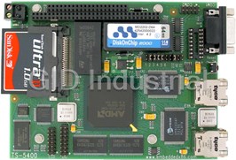
Technologic Systems TS-5400 CPU Board with AMD 133 MHz 5x86 processor, 2 COM ports, 2 Ethernet, Comp...
Technologic Systems TS-5500 CPU Board with AMD 133 MHz 5x86 processor, PCMCIA, 3 COM, Ethernet, Comp...
Technologic Systems TS-5500-64 CPU Board with AMD 133 MHz 5x86 processor, PCMCIA, 3 COM, Ethernet, C...
Technologic Systems TS-5600 CPU Board with AMD 133 MHz 5x86 processor, PCMCIA, 2 COM, Ethernet, Comp...
Technologic Systems TS-5700 CPU Board with AMD 133 MHz 5x86 processor, PCMCIA, 4 COM, Ethernet, Comp...
Technologic Systems TS-7200 CPU Board with ARM 200 MHz processor, 2 COM, 2 USB, Ethernet, Compact Fl...
Request a Quote

The quote request has been received
Close

Facing challenges or have inquiries? Feel free to contact us!
Call Us +1-469-283-2440
What they say about us
FANTASTIC RESOURCE
One of our top priorities is maintaining our business with precision, and we are constantly looking for affiliates that can help us achieve our goal. With the aid of GID Industrial, our obsolete product management has never been more efficient. They have been a great resource to our company, and have quickly become a go-to supplier on our list!
Bucher Emhart Glass
EXCELLENT SERVICE
With our strict fundamentals and high expectations, we were surprised when we came across GID Industrial and their competitive pricing. When we approached them with our issue, they were incredibly confident in being able to provide us with a seamless solution at the best price for us. GID Industrial quickly understood our needs and provided us with excellent service, as well as fully tested product to ensure what we received would be the right fit for our company.
Fuji
HARD TO FIND A BETTER PROVIDER
Our company provides services to aid in the manufacture of technological products, such as semiconductors and flat panel displays, and often searching for distributors of obsolete product we require can waste time and money. Finding GID Industrial proved to be a great asset to our company, with cost effective solutions and superior knowledge on all of their materials, it’d be hard to find a better provider of obsolete or hard to find products.
Applied Materials
CONSISTENTLY DELIVERS QUALITY SOLUTIONS
Over the years, the equipment used in our company becomes discontinued, but they’re still of great use to us and our customers. Once these products are no longer available through the manufacturer, finding a reliable, quick supplier is a necessity, and luckily for us, GID Industrial has provided the most trustworthy, quality solutions to our obsolete component needs.
Nidec Vamco
TERRIFIC RESOURCE
This company has been a terrific help to us (I work for Trican Well Service) in sourcing the Micron Ram Memory we needed for our Siemens computers. Great service! And great pricing! I know when the product is shipping and when it will arrive, all the way through the ordering process.
Trican Well Service
GO TO SOURCE
When I can't find an obsolete part, I first call GID and they'll come up with my parts every time. Great customer service and follow up as well. Scott emails me from time to time to touch base and see if we're having trouble finding something.....which is often with our 25 yr old equipment.
ConAgra Foods