

 Manufacturers
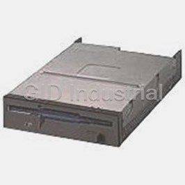
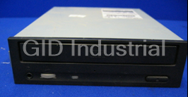
TEAC FD235HFC929
Description
TEAC 3.5" floppy disk drive; w/ jumpers (Black)
Part Number
FD235HFC929
Price
Request Quote
Manufacturer
TEAC
Lead Time
Request Quote
Category
TBD
Features
- A choice of models and interface type ( TTL or CMOS ) to match your system requirements
- Low power consumption ( Operating:1.4W )
- One-inch high design
- Operates on +5v power
Datasheet

Extracted Text
TEAC FD-235HF-C929/C940/C991 MICRO FLOPPY DISK DRIVE SPECIFICATION Rev. A 35 sheets in Total 7331 TABLE OF CONTENTS Title Page 1. OUTLINE ..................................................................................................................................... 1 2. DISK ............................................................................................................................................ 2 3. PHYSICAL SPECIFICATION ...................................................................................................... 3 4. OPERATIONAL CHARACTERISTICS ....................................................................................... 5 4.1 2MB Mode Data Capacity ..................................................................................................... 5 4.2 1MB Mode Data Capacity ..................................................................................................... 6 4.3 Disk Rotation Mechanism .................................................................................................... 6 4.4 Index Detection ..................................................................................................................... 7 4.5 Track Construction ............................................................................................................... 7 4.6 Magnetic Head ....................................................................................................................... 7 4.7 Track Seek Mechanism ......................................................................................................... 8 4.8 Window Margin and Others .................................................................................................. 8 5. ENVIRONMENTAL CONDITIONS .............................................................................................. 9 6. RELIABILITY ............................................................................................................................. 10 7. POWER INTERFACE ................................................................................................................ 11 7.1 Required Power ................................................................................................................... 11 7.2 Power Interface Connector and Cable .............................................................................. 12 8. SIGNAL INTERFACE ................................................................................................................ 14 8.1 Signal Interface Connector and Cable .............................................................................. 14 8.2 Electrical Charactristics ..................................................................................................... 16 8.2.1 FDD side receiver and driver ........................................................................................ 16 8.2.2 Host side receiver and driver ....................................................................................... 16 8.3 Input/Output Signals ........................................................................................................... 18 8.3.1 DRIVE SELECT input signal ......................................................................................... 18 8.3.2 MOTOR ON input signal ............................................................................................... 18 8.3.3 DIRECTION SELECT input signal ................................................................................ 18 8.3.4 STEP input signal .......................................................................................................... 18 8.3.5 WRITE GATE input signal ............................................................................................. 18 8.3.6 WRITE DATA input signal ............................................................................................. 19 8.3.7 SIDE ONE SELECT input signal ................................................................................... 19 8.3.8 TRACK 00 output signal ............................................................................................... 19 8.3.9 INDEX output signal ...................................................................................................... 19 8.3.10 READ DATA output signal .......................................................................................... 20 8.3.11 WRITE PROTECT output signal ................................................................................. 20 8.3.12 DISK CHANGE output signal ...................................................................................... 20 8.3.13 READY output signal .................................................................................................. 20 8.3.14 Input/Output signals for density mode setting (HD IN/HD OUT) ............................. 20 8.3.15 NO CONNECTION (NC) ............................................................................................... 21 8.3.16 Treatment of not-used signals ................................................................................... 22 9. CONTROL SEQUENCE ............................................................................................................ 24 9.1 Power-on .............................................................................................................................. 24 9.2 Seek Operation .................................................................................................................... 25 9.3 Read Write Operation ......................................................................................................... 26 9.4 Current Consumption Profile ............................................................................................. 27 10. FRAME GROUNDING ............................................................................................................. 29 11. CUSTOMER SELECTABLE STRAPS .................................................................................... 30 – i – 11.1 Function Summary of Straps ........................................................................................... 30 11.2 DS0/DS1 Straps ................................................................................................................. 30 11.3 HA/HI2/HO2 Straps ............................................................................................................ 31 11.4 RY34/DC34 Straps ............................................................................................................. 31 11.5 FG Strap ............................................................................................................................. 31 12. TURN ON CONDITION OF INDICATOR AND SPINDLE MOTOR ......................................... 32 12.1 Front Bezel Indicator ........................................................................................................ 32 12.2 Spindle Motor .................................................................................................................... 32 – ii – 1. OUTLINE This specification provides a description for the TEAC FD-235HF, dual density (2/1MB, 2-modes), 90mm (3.5-inch) micro floppy disk drive (hereinafter referred to as FDD). Table 1-1 shows the outline of the FDD, and Table 1-2 shows the signal interface pin-assignment. (Table 1-1) Specification outline Model name FD-235HF-C929 FD-235HF-C940 FD-235HF-C991 Front bezel Black Beige (AT) Beige (PS) Eject button Black Beige (AT) Beige (PS) LED indicator Green Safety standard UL, CSA & TÜV Operation modes 2MB mode 1MB mode Write and read Write and read 90mm (3.5-inch) disk used High density Normal density (2HD) (2DD) Unformatted data capacity 2M bytes 1M bytes Data transfer rate 500k bits/s 250k bits/s Disk rotational speed 300rpm 300rpm Track density 5.3track/mm (135tpi) Track to track time 3ms Required power +5V single (4.5 ~ 5.5V) Signal output driver Open collector TTL Input signal pull-up 1kΩ ±5%, unremovable Customer selectable strap 8 selections (DS0, DS1, RY34, DC34, HO2, HI2, HA, FG) Refer to item 11.1 Function setting at delivery 1. Strap setting 1.1 DS1 : DRIVE SELECT 1 on pin 12 1.2 DC34 : DISK CHANGE on pin 34 1.3 HA : Automatic density setting for 2DD (1MB) disk or 2HD (2MB) disk. 1.4 FG : Frame is electrically shorted to DC 0V. 2. Other interface setting 2.1 Pin2 : Open 3. Other function setting 3.1 LED turn on condition: DRIVE SELECT 3.2 Motor rotating condition: MOTOR ON 3.3 Ready and seek-complete gate (full-mask) for INDEX and READ DATA output pulses. 3.4 Auto-chucking at disk installation 3.5 Auto-recalibration at power on Interface connector 34 pin right-angled header connector Power connector Equipped Other optional function Not equipped – 1 – (Table 1-2) Signal interface pin-assignment Pin Nos. Signals Pin Nos. Signals Direc 1 NC 2 HD IN (HD at HIGH level)/HD OUT Input/ (HD at HIGH level)-OPEN Output 3NC4 NC – 5NC6 NC Input 7 0V 8 INDEX Output 9 0V 10 DRIVE SELECT 0/OPEN Input 11 0V 12 DRIVE SELECT 1/OPEN Input 13 0V 14 NC Input 15 0V 16 MOTOR ON Input 17 0V 18 DIRECTION SELECT Input 19 0V 20 STEP Input 21 0V 22 WRITE DATA Input 23 0V 24 WRITE GATE Input 25 0V 26 TRACK 00 Output 27 0V 28 WRITE PROTECT Output 29 0V 30 READ DATA Output 31 0V 32 SIDE ONE SELECT Input 33 0V 34 DISK CHANGE/READY Output The FDD is equipped with a discrimination switch for the high density (HD) hole of an installed disk cartridge. Refer to item 8.3.13 as to the detailed explanation for density mode setting. 2. DISK (1) Work disk 90mm (3.5-inch) micro floppy disks which are mutually agreed between the customer and TEAC. For 2MB mode : High density disk (2HD) 1MB mode : Normal density disk (2DD) (2) Cleaning disk The FDD does not require any cleaning disk. However, the dry type disk is used when requiring a clean- ing disk. – 2 – 3. PHYSICAL SPECIFICATION (Table 3-1) Physical specification Width 101.6mm (4.00 in), Nom. Height 25.4mm (1.00 in), Nom. Depth 145mm (5.71 in), Nom., excluding front bezel Weight 410g (0.90lbs), Nom., 415g (0.91 lbs), Max. External view See Fig. 3-1. Cooling Natural air cooling Mounting Mountings for the following directions are acceptable. (a) Front loading, mounted vertically. (b) Front loading, mounted horizontally with spindle motor down. (c) The mounting tilt in items (a) and (b) should be 25° or less with the front bezel up (+) or down (-). However, the disk must not be allowed to eject out of the tray with the tilt from the horizontal level to +25°. Note: Mounting directions other than the above will be considered separately. Installation With installation holes on the frame of the FDD. Refer to Fig. 3-1. Material of flame Sheet metal Material of front bezel PPHOX or ABS (applied to HF-C591 and HF-C529) (Complying with UL94-5V) – 3 – (Fig. 3-1) FDD external view – 4 – 4. OPERATIONAL CHARACTERISTICS 4.1 2MB Mode Data Capacity (Table 4.1-1) 2MB mode data capacity Recording method FM MFM Data transfer rate k bits/s 250 500 Tracks/disk 160 160 Innermost track bit density bpmm (bpi) 343.19 686.38 (8,717) (17,434) Innermost track flux density frpmm (frpi) 686.38 686.38 (17,434) (17,434) k bytes/track 6.25 12.5 Unformatted k bytes/disk 1,000 2,000 k bytes/sector 0.128 0.256 32 sectors/track k bytes/track 4.096 8.192 k bytes/disk 655.36 1,310.72 Data k bytes/sector 0.256 0.512 capacity 18 sectors/track k bytes/track 4.608 9.216 k bytes/disk 737.28 1,474.56 k bytes/sector 0.512 1.024 10 sectors/track k bytes/track 5.12 10.24 k bytes/disk 819.2 1,638.4 – 5 – Formatted 4.2 1MB Mode Data Capacity (Table 4.2-1) 1MB mode data capacity Recording method FM MFM Data transfer rate k bits/s 125 250 Tracks/disk 160 160 Innermost track bit density bpmm (bpi) 171.61 343.19 (4,359) (8,717) Innermost track flux density frpmm (frpi) 343.19 343.19 (8,717) (8,717) k bytes/track 3.125 6.25 Unformatted k bytes/disk 500 1,000 k bytes/sector 0.128 0.256 16 sectors/track k bytes/trac 2.048 4.096 k bytes/disk 327.68 655.36 Data k bytes/sector 0.256 0.512 capacity 9 sectors/track k bytes/track 2.304 4.608 k bytes/disk 368.64 737.28 k bytes/sector 0.512 1.024 5 sectors/track k bytes/track 2.56 5.12 k bytes/disk 409.6 819.2 4.3 Disk Rotation Mechanism (Table 4.3-1) Disk Rotation Mechanism Spindle motor DC brushless motor Spindle speed 300rpm Motor servo method Frequency servo by ceramic oscillator Motor/spindle connection Motor shaft direct Disk speed The same as the spindle speed. Long term speed variation (LSV) ±1.5% or less Instantaneous speed variation (ISV) ±2% or less Start time 480ms or less Average latency 100ms Ready waiting time 505ms or less for motor on – 6 – Formatted 4.4 Index Detection (Table 4.4-1) Index Detection Number of index 1 per disk revolution Detection method Rotor detection of spindle motor by Hall element or FG output. Detection cycle 200ms ±1.5% Index burst detecttion timing error ±400µs or less (with specified test disk) 4.5 Track Construction (Table 4.5-1) Track Construction 5.3 tracks/mm (135tpi) Track density Track pitch 187.5µm Number of cylinders 80 cylinders Number of tracks 160 tracks/disk Side 0 39.500mm (1.5551 in) Outermost track radius (track 00) Side 1 38.000mm (1.4961 in) Side 0 24.6875mm (0.9719 in) Innermost track radius (track 79) Side 1 23.1875mm (0.9129 in) Positioning accuracy ±15µm or less, with specified test disk (Track 40, 23 ± 2°C, 45 ~ 55%RH, horizontal) 4.6 Magnetic Head (Table 4.6-1) Magnetic Head Magnetic head Read/write head with erase gap, 2 sets Effective track width after trim erase 0.115 ± 0.008mm (0.0045 ± 0.0003 in) Read/write gap azimuth error 0° ± 18’, with specified test disk – 7 – 4.7 Track Seek Mechanism (Table 4.7-1) Track Seek Mechanism Head position mechanism Stepping motor and lead screw Stepping motor 4-phase, 20 steps per revolution Stepping motor drive 2 steps per track Track 00 detection method Photo-interrupter Track to track time 3ms (excludes settling time, refer to item 8.3.4) Settling time 15ms or less (excludes track to track time) Average track seek time 94ms (includes settling time) 4.8 Window Margin and Others (Table 4.8-1) Window Margin and Others Window Margin (with specified test disk, MFM method , PLL separator) 2MB mode 300ns or more 1MB mode 600ns or more Recommendable write pre-compensation 2MB mode ±125ns 1MB mode 0 ~ ±125ns Head load mechanism Not equipped (The FDD becomes head load condition whenever a disk is installed.) File protect mechanism Detection of write inhibit hole by switch Disk detection mechanism Detection of disk installation by switch Disk inserting force 6.86N (700g) or less at the center of disk Disk ejecting force 13.73N (1400g) or less Acoustic noise at 50cm 50dBA or less at 3ms or 4ms seek operation Disk type descriminating mechanism Detection of HD hole by switch – 8 – 5. ENVIRONMENTAL CONDITIONS (Table 5-1) Environmental Condition Operating Storage Transportation 4 ~ 51.7°C (39 ~ 125°F) –22~60°C (–8 ~ 140°F) Ambient temperature –40 ~ 65°C (–40 ~ 149°F) Temperature gradient 20°C (36°F) or less per 30°C (54°F) or less per 30°C (54°F) or less per hour hour hour Relative humidity 20 ~ 80% 5 ~ 90% 5 ~ 95% (no condensation) Max. (no condensation) Max. (no condensation) Max. wet bulb temperature wet bulb temperature wet bulb temperature shall be 29.4°C (85°F) shall be 40°C (104°F) shall be 45°C (113°F) 2 2 14.7m/s (1.5G) or less 19.6m/s (2G) or less (10 ~ 100Hz, 1 octave/ (10 ~ 100Hz, 1/4 octave/ min sweep rate) min sweep rate) 2 9.8m/s (1.0G) or less Vibration —— (100 ~ 200Hz, 1 octave/ min sweep rate) 2 4.9m/s (0.5G) or less (200 ~ 600Hz, 1 octave/ min sweep rate) 2 2 Write & read: 49m/s 686m/s (70G) —— (5G)(11ms, 1/2 sine (11ms, 1/2 sine wave) or wave) or less less Shock 2 Read only: 98m/s (10G)(11ms, 1/2 sine —— wave) or less –300m (–980feet) ~ —— 5,000m (16,400feet) Altitude Notes: The above requirements are applied for the FDD without shipping box. When a long period is required for transportation such as by ship, storage environmental conditions should be applied. – 9 – 6. RELIABILITY (Table 6-1) Reliability MTTF 30,000 power on hours or more (for typical operation duty) MTTR When failure, the FDD should be replaced in unit of the drive and not repaired in unit of parts or assemplies. Design component life 5 years 6 Disk life 3 × 10 passes/track or more 4 Disk insertion 1.5 × 10 times or more 7 Seek operation 1 × 10 random seeks or more Preventive maintenance Not required (for typical operation duty) 9 Soft error 1 or less per 10 bits read A soft (recoverable) error means that it can be recoverred correcty within three retries. 12 Hard error 1 or less per 10 bits read A hard (unrecoverable) error means that it cannot be recovered Error rate correstly within three retries. However, it is recommended to be followed by a recalibration to track 00 and four additional retries. 6 Seek error 1 or less per 10 seeks A seek error means that it can seek to a target track within one retry including a recalibration to track 00. Safety standard Approved by UL, CSA and TÜV Electro-static dischange test 15kV (150pF, 330Ω) No hard error and/or no component damage occur when the test is applied to the operator access area (front bezel area). – 10 – 7. POWER INTERFACE 7.1 Required Power The following specifications are applied at interface connector of the FDD. (1) DC +12V : Not required (2) DC +5V (a) Voltage tolerance :±10% (4.5 ~ 5.5V) (b) Allowable ripple voltage :100mVp-p or less (including spike noise) (c) Current and power consumption (Table 7.1-1) Current and power consumption Operating mode Average current Average power Typ. Max. Typ. Max. Stand-by 8mA 10mA 40mW 55mW Read operation 0.30A 0.40A 1.50W 2.20W Write operation 0.30A 0.40A 1.50W 2.20W 3ms 0.56A 0.66A 2.80W 3.63W Seek operation 6ms 0.60A 0.70A 3.30W 4.18W Seek operation peak 0.9A 1.0A 4.50W 5.50W Spindle motor start 0.62A 0.70A 3.10W 3.85W Notes: 1. Values of Typ. current and power are specified at 5.0V, while the values of Max. are at 5.5V (+10%) with a disk of large running torque. 2. Stand-by mode is defined at the stop condition of spindle motor and seek operation. 3. Seek operation peak means the operation during the settling (15ms) after the seek conpletion. 4. Rush current flows within 150ms after the motor start. 5. Short time peak current except for power-on surge is less than 1.0A. 6. Refer to item 9.4 as to the current consumption profile. – 11 – 7.2 Power Interface Connector and Cable (1) Power interface connector (Table 7.2-1) Power interface connector FDD side connector TEKCON, P/N 1603-823-04R-54 or equivalent Pin numbers 4 pins Protection method for mis- Mechanical protection by the shape of connector housing connection Connector external view See Fig. 7.2-1. Connector location See Fig. 3-1. Power interface connections See Table 7.2-2. Cable side matched AMP P/N 171822-4 (natural color) or equivalent connector Cable side matched pin AMP P/N 170204-2 (AWG#20 ~ 26, loose piece) or P/N 170262-2 (AWG#20 ~ 26, strip form) or equivalent (2) Power interface cable: Any appropriate cables taking the maximum power consumption of the FDD will be acceptable. (Table 7.2-2) Power interface pin-assignment Power voltage Pin numbers DC +5V 1 0V 2 (0V) 3 (No conection) 4 – 12 – Power interface connector 32 4 1 Pin number Upper side of the FDD PCB Rear view 1 43 2 FDD side Cable side Cable Top view (Fig. 7.2-1) Power interface connector external view – 13 – 8. SIGNAL INTERFACE 8.1 Signal Interface Connector and Cable (1) Signal interface connector (Table 8.1-1) Signal interface Connector FDD side connector I-PEX, P/N 5003-001-0346F or equivalent Pin numbers and pin pitch 2.54mm (0.1 in) pitch, 34-pin block header (17-pin double rows, even number pins are upper side of the FDD). Connector external view See Fig. 8.1-1. Connector location See Fig. 3-1. Cable side matched FUJITSU, P/N FCN-747B034-AU/B (closed end) or -AU/O (daisy connector chain) or equivalent. Note: It is recommanded to use a polarizing type connector with a projection on the center of the housing to avoid mis-connection. Refer to Fig. 8.1-1. For such a polarizing connector, ∇mark of the connector housing may show pin No.34. (2) Signal interface cable Maximum cable length :1.5m (5 feet), by terminator of 1kΩ or less (For daisy chain connection, the total cable length should be less than 1.5m). – 14 – Signal interface connector Upper side of the FDD 34 Pin numbers 2 1 33 Rear view Lower side of the FDD FDD side signal interface connector 2 34 Projection (upper side) Cable side signal interface connector Top view Side view (Fig. 8.1-1) Signal interface connector external view – 15 – 8.2 Electrical Charactristics “Vcc” means +5V power voltage supplied to the FDD. 8.2.1 FDD side receiver and driver The specification are applicable at the interface connector of the FDD. (Table 8.2.1-1) FDD side receiver and driver Interface driver/reciver See Fig. 8.2-1. LOW level (TRUE) 0 ~ 0.7V Input signals LOW level input current 5.9mA, Max. (Including terminator (TTL level) current) Electrical characteristics of HIGH level (FALSE) 2.2V ~ +5V power voltage receiver Terminator resistor value 1kΩ ±5% Terminator (pull-up) resistor is connected to each input. LOW level (TRUE) 0 ~ 0.4V Electrical Output signals Driver sink current 37mA, Max. characteristics of (Open collector capability driver driver) HIGH level (FALSE) Depending on host side terminator 8.2.2 Host side receiver and driver (Table 8.2.2-1) Host side receiver and driver Host side driver TTL, CMOS, etc. Driver required sink current FDD input current × Number of daisy chained FDD Host side receiver TTL, CMOS, etc. Terminator is required for each output signal line from the FDD. Host side terminator resistor value Usually 1 ~ 2.2kΩ is used. (150Ω Min.) – 16 – FDD PCB Ass’y Control & R/W LSI (Bi-CMOS) Strap block FG 0V FG DS0 10 10P DRIVE SELECT 0 Select DS 12 DRIVE SELECT 1 DS1 RY 12P Ready RY34 DC34 DISK CHANGE/ 34 34P Disk change DC READY HA HI HS HD in HI2 HO2 HO 2 HD IN/HD OUT HD sensor Terminators 5V Other input signals Other output signals Open collector drivers (Fig. 8.2-1) FDD signal interface circuit – 17 – 8.3 Input/Output Signals In the following, input signals are those transmitted to the FDD while output signals are those transmitted from the FDD. LOW level of the signals is TRUE unless otherwise specified. Refer to Table 1-2 as to the signal needed in this specification. 8.3.1 DRIVE SELECT input signal (1) Signal to select a specific FDD for operation in multiplex control. (2) Only the DRIVE SELECT signal of the same number as of on-state strap is effective. (3) All the input/output signals except for the MOTOR ON and HD IN are valid after this signal is made TRUE. The time required to be valid is 0.5µsec, Max. including transmission delay time of the DRIVE SELECT signal through the interface cable. (4) Refer to item 11.1 as to the turn-on condition of the front bezel indicator. (5) Refer to item 11. and Table 1-2 as to the strap setting and the selection of signal function. 8.3.2 MOTOR ON input signal (1) Level signal to rotate the spindle motor. (2) The spindle motor reaches to the rated rotational speed (300rpm) within 480ms after this signal is made TRUE. (3) Refer to item 11.2 as to the rotational condition of the spindle motor. 8.3.3 DIRECTION SELECT input signal (1) Level signal to define the moving direction of the head when the STEP line is pulsed. (2) Step-out (moving away from the center of the disk) is defined as HIGH level of this signal. Conversely, step-in (moving toward the center of the disk) is defined as LOW level of this signal. (3) The signal shall maintain its level for 0.8µs, Min. prior to the trailing edge of the STEP pulse. Refer to Fig. 9.2-1. 8.3.4 STEP input signal (1) Negative pulse signal to move the head. The pulse width shall be 0.8µs or more and the head moves one track space per one pulse. (2) The access motion (head seek operation) is initiated at the trailing edge of the STEP pulse and completes within 18ms after starting the access including the settling time. (3) For the subsequent motion in the same direction, the STEP pulses should be input with the interval of 3ms or more, while the pulses should be input with the interval of 4ms or more for a direction change. Refer to Fig. 9.2-1. STEP pulses less than 3ms interval for the same direction or less than 4ms interval for a direction change may cause seek error. (4) STEP pulses are ignored and the access motion is not initiated when one of the following conditions is satisfied. (a) The WRITE PROTECT signal is FALSE and the WRITE GATE signal is TRUE. (b) The TRACK 00 signal is TRUE and the DIRECTION SELECT signal is HIGH level (step-out). (c) Step-in operation (DIRECTION SELECT signal is LOW level) from track 81. 8.3.5 WRITE GATE input signal (1) Level signal to erase the written data and to enable the writing of new data. (2) The FDD is set to write mode when the following logical expression is satisfied. WRITE GATE * DRIVE SELECT * WRITE PROTECT – 18 – (3) This signal shall be made TRUE after satisfying all of the following conditions. (a) 18ms has been passed after the effective receival of the final STEP pulse. (b) 100µs has been passed after the level change of the SIDE ONE SELECT signal. (4) The following operations should not be done at least 650µs after this signal is changed to FALSE. (a) Make the MOTOR ON signal FALSE. (b) Start the head seek operation by the STEP pulse. (c) Make the DRIVE SELECT signal FALSE. (d) Change the level of the SIDE ONE SELECT signal. (e) Change the level of the HD IN signal. 8.3.6 WRITE DATA input signal (1) Negative pulse signal to designate the contents of data to be written on a disk. The pulse width should be 0.1µs through 1.1µs and the leading edge of the pulse is used. (2) WRITE DATA pulses are ignored while either of the following conditions is satisfied. (a) The WRITE GATE signal is FALSE. (b) The WRITE PROTECT signal is TRUE. (3) This signal should be input according to the timing in Fig. 8.3-2. It is recommended to stop the input of the WRITE DATA pulses during the read operation in order to avoid harmful cross talk. 8.3.7 SIDE ONE SELECT input signal (1) Level signal to designate which side of a double sided disk is used for reading or writing. (2) When this signal is HIGH level, the magnetic head on the side 0 surface (lower side) of the disk is selected, while the magnetic head on the side 1 surface (upper side) is selected when this signal is LOW level. (3) The READ DATA pulse on a selected surface is valid more than 100µs after the change of this signal level. (4) Write operation (the WRITE GATE signal is TRUE) on a selected surface shall be started more than 100µs after the change of this signal level. 8.3.8 TRACK 00 output signal (1) Level signal to indicate that the head is on track 00. (2) This signal is valid more than 2.8ms, after the effective receival of the STEP pulse. 8.3.9 INDEX output signal (1) Negative pulse signal to indicate the start point of a track and one index pulse per one disk revolution is output. (2) INDEX pulse is output when the following logical expression is satisfied. Index detection * DRIVE SELECT * Ready state * Seek-complete Notes: (a) Ready state: • The FDD is powered on. • A disk is installed. • Auto-chucking completed. • A motor-on command is TRUE and 505ms, approx. has been passed. • An INDEX pulse has been detected after motor-on command. • Change the level of the HD IN signal when the strap is on-state. (b) Seek-complete means the state that 15.8 ~ 17.9ms has been passed after the trailing edge of the – 19 – final STEP pulse. (3) Fig. 8.3-1 shows the timing of this signal. Leading edge of the pulse shall be used as the reference and pulse width is 1.5ms through 5ms. 8.3.10 READ DATA output signal (1) Negative pulse signal for the read data from a disk composing clock bits and data bits together. (2) Fig. 8.3-3 shows the timing of this signal. Pulse width is 0.15µs through 0.8µs and the leading edge of the pulse shall be used as the reference. (3) READ DATA pulse is output when the following logical expression is satisfied. Read data detection * DRIVE SELECT * Write operation * Ready state * Seek-complete Notes: (a) Refer to item 8.3.9 as to the ready state. (b) Write operation is the state while the WRITE GATE input signal is FALSE and erase delay time has been passed after the WRITE GATE signal changed to FALSE. (c) Refer to item 8.3.9 as to the seek-complete. (4) Output pulse is valid while all of the following conditions are satisfied. (a) 18ms has been passed after the effective receival of the final STEP pulse. (b) 100µs has been passed after the level change of the SIDE ONE SELECT signal. (c) 650µs (2MB mode) or 690µs (1MB mode) has been passed after the WRITE GATE signal is changed to FALSE. 8.3.11 WRITE PROTECT output signal (1) Level signal to indicate that the write inhibit hole of an installed disk is open. (2) When this signal is TRUE, data on the disk are protected from miserasing and write operation is inhibited. 8.3.12 DISK CHANGE output signal (1) Level signal to indicate that a disk in the FDD is ejected. (2) Refer to item 11. for the strap setting of this signal. (3) This signal changes to TRUE when either of the following conditions is satisfied. (a) Power on. (b) A disk is removed. (4) The signal returns to FALSE when both of the following conditions are satisfied. Refer to Fig. 8.3-4. (a) A disk has been installed. (b) A STEP command is received when the DRIVE SELECT signal is TRUE. 8.3.13 READY output signal (1) Level signal to indicate that the FDD is in ready state (refer to item 8.3.9) for read and write operations. (2) Refer to item 11 as to the strap setting for this signal output. (3) Required time for this signal to be TRUE after the start of the spindle motor is 505ms, Max. (4) When a motor-on command is made FALSE, this signal is also changed to FALSE within 0.3ms. 8.3.14 Input/Output signals for density mode setting (HD IN/HD OUT) Every FDD model, there are any basic methods for setting the density mode of the FDD as shown in the following. Use the applicable method for the FDD in contents shown below. (1) Method A using HD IN input signal (a) HIGH or LOW level of the HD IN signal from host controller is used to designate the density mode of the FDD. There is no output signal from the FDD for disk type identification. (b) Table 8.3.14-1 shows the meaning of the logic level. – 20 – (2) Method B without using any interface signal (OPEN) (a) Interface signal is not used between the FDD and host-controller. Density mode of the FDD and host system are determined independently. (b) Density mode of the FDD is automatically set by discriminating the HD hole of an installed disk. If the density mode of the FDD is not coincident with that of the host controller, data errors always occur at read operation. (c) It can not be selected when the HD IN input signal is setted to HIGH DENSITY at LOW level. (3) Method C using HD OUT output signal (a) Density mode of the FDD is automatically set by discriminating the HD hole of an installed disk. (b) HIGH or LOW level of the HD OUT signal from the FDD is used to inform host controller which type of disk is installed in the FDD. And the density mode of the host is automatically determined according to this signal. (c) Table 8.3.14-1 shows the meaning of the logic level. (d) It can not be selected when the HD IN input signal is setted to HIGH DENSITY at LOW level. (4) Method D using HD IN/HD OUT signals (a) HIGH or LOW level of the HD OUT signal from the FDD is used to inform host controller which type of disk is installed in the FDD. Refer to method C. On the other hand, the density mode of the FDD is set by the HIGH or LOW level of the HD IN signal from the host. Refer to method A. (b) Usually both of the density mode of the FDD and the host are the determined according to an installed disk type like method C. For a special case, however, that on installed disk had already been written at unsuitable density, the system can forced (or over write) only using the HD IN signal by operator designation. (c) Table 8.3.14-1 shows the meaning of the logic level. (Table 8.3.14-1) Meaning of the logic level Signal name Logic level HIGH DENSITY at HIGH LEVEL HIGH DENSITY at LOW LEVEL HIGH 2MB mode 1MB mode HD IN LOW 1MB mode 2MB mode HIGH 2HD disk or no disk 2DD disk HD OUT LOW 2DD disk 2HD disk or no disk 8.3.15 NO CONNECTION (NC) The NC pins are electrically isolated from any other circuit in the FDD. – 21 – 8.3.16 Treatment of not-used signals If some of the provided input/output signals are not necessary for your application, keep the unused signal lines open or pull up by an appropriate resistor value (refer to item 8.2.2) at the host side. 1.5 ~ 5ms INDEX 197 ~ 203ms (300rpm) (Fig. 8.3-1) INDEX timing WRITE GATE 111 00 01 WRITE DATA Magnetization on disk 0.1 ~ 1.1µs 2F 4/3F 1F 4/3F t1 8µs t2 t2 t3 8µs * : ±0.5% Max. Max. * * * * Density mode rpm t1 t2 t3 2MB mode 300 2µs, Nom. 3µs, Nom. 4µs, Nom. 1MB mode 300 4µs, Nom. 6µs, Nom. 8µs, Nom. (Fig. 8.3-2) WRITE DATA timing (MFM method) Magnetization on disk 11 0 01 0 1 READ DATA 0.15 ~ 0.8µs 2F 4/3F 1F 4/3F t4 t5 t5 t6 – 22 – ~ ~ ~ ~ ~ ~ Density mode rpm t4t5t6t7 2MB mode 300 2µs, Nom. 3µs, Nom. 4µs, Nom. ±350ns 1MB mode 300 4µs, Nom. 6µs, Nom. 8µs, Nom. ±700ns (Fig. 8.3-3) READ DATA timing (MFM method) Power on Disk eject Disk install Installed Installed Disk installation Ejected STEP DISK CHANGE 1µs, Max. 1µs, Max. Note: To simplify the timing chart, the DRIVE SELECT signal is assumed always TRUE in the above figure. (Fig. 8.3-4) DISK CHANGE signal timing – 23 – 9. CONTROL SEQUENCE 9.1 Power-on (1) Protection against power on and off (a) In the transient period when the +5V power is lower than 3.5V, the FDD is protected against miswriting and miserasing whatever the state of input signals are. (b) Except for the condition of item (a), the FDD is protected against miswriting and miserasing as long as the WRITE GATE input signal does not change to TRUE. (2) Power reset time in FDD: Less than 400ms, including auto-recalibration 3.5 ~ 4.4V +5V power Valid interface signals Valid Power resetting 400ms, Max. with auto-recalibration Internal miswrite protection (Fig. 9.1-1) Power on sequence – 24 – 9.2 Seek Operation Seek operation can be done independently of the spindle motor rotation. t1 t1 t1 t1 DRIVE SELECT Step-out Step-in DIRECTION SELECT STEP t1 t2 t1 t1 t1 t1 650µs 3ms 4ms, Min. 3ms Min. Min. Min. WRITE GATE TRACK 00 2.8ms, Max. 1µs, Max. t1 ≥ 0.8µs t2 ≥ 2µs (Fig. 9.2-1) Seek operation timing – 25 – ~ ~ ~ ~ ~ ~ ~ ~ ~ ~ ~ ~ ~ ~ 9.3 Read Write Operation (650µs, Min.) MOTOR ON (650µs, Min.) DRIVE SELECT 500ms, Max. 0.3ms, Max. READY Valid INDEX 15.8~17.9ms (Seek-complete) STEP 650µs, Min. 3ms, Min. WRITE GATE 8µs, Max. 8µs, Max. WRITE DATA 18ms, Min. (650µs,Min.) 0, Min. 0, Min. 650µs,Max. (2MB mode) 100µs, Min. 690µs,Max. (1MB mode) SIDE ONE SELECT 100µs, Max. 100µs, Max. READ DATA Valid Valid Valid Valid 15.8~17.9ms (Seek-complete) Other input signals Valid Other output signals Valid 0.5µs, Max. (Fig. 9.3-1) Read/Write operation timing – 26 – 9.4 Current Consumption Profile +5V typical average current mA High current (350ms, Max.) 15ms 800 from the last step 600 400 200 0 Initial reset Auto-recalibration Stand Stand FDD status Read Seek Stand-by Read Write Read -by -by Motor start Drive selected Auto-chucking Disk Power installation on Motor-on command DRIVE SELECT STEP Start rush Spindle motor power 0 Steppin motor power 0 Read write on off amp. power on Logic power – off (Fig. 9.4-1) Typical average current profile – 27 – (1) Stand-by mode When both of the following conditions are satisfied, FDD goes to the stand-by mode (low power con- sumption mode). (a) The spindle motor stops. (b) Not in the seek operation (including the settling time). Note: In the stand-by mode, the FDD can immediately respond to a command from host controller with no restriction. If the polling operation of the DRIVE SELECT line is done in the stand-by mode, current flows intermittently and +5V current slightly increases. (2) Simultaneous operation of motor start and seek If a seek operation is done during the start-up of the spindle motor, or if the motor starts during the seek operation, +5V current at motor start increases by 0.55A, Max. from the value in Table 7.1-1. Stepping motor is energized at high power from the first STEP to 15msec after the last STEP. (3) +5V current increases for 15ms after a lapse of 500ms by engergizing of the motor. – 28 – 10. FRAME GROUNDING (1) The FDD frame is electrically connected to DC 0V by the FG strap on the main PCBA. (See Fig. 10-1) (2) If it is required to separate the FDD frame from DC 0V, remove the FG strap. However, the FDD frame must be electrically connected to DC 0V by some other method when the FDD is tested alone. (3) If it is required to connect the FDD frame to the host side by other cabling method, M2.6 tapped hole at the rear side of the FDD can be used. (See Fig. 3-1). FDD Main PCBA FG strap Interface connector (0V) Frame ground tapped hole (M2.6) PCBA mounting screw (Fig. 10-1) Frame ground internal connection – 29 – 11. CUSTOMER SELECTABLE STRAPS 11.1 Function Summary of Straps The FDD is equipped with the following selectable straps on the main PCBA. Insertion of a short bar onto the post pin is defined as the on-state of the strap. Refer to Table 1-1 in item 1. as to the strap setting at delivery and selectable straps. DS1 HI2 1 FG DS 12 DC HI 2 HA DS0 DC34 HO2 FG RY34 2 0V 10 RY 34P HS HO Strap post layout A BC D E F (Table 11.1-1) Function summary straps Strap Function DS0 DRIVE SELECT 0 input on pin 10 DS1 DRIVE SELECT 1 input on pin 12 *RY34 READY output on pin 34 *DC34 DISK CHANGE output on pin 34 *HA Density set automatically *HI2 Density set by HD IN on pin 2 *HO2 HD OUT output on pin 2 FG Short between FDD frame and DC 0V Notes : *straps overlap with other strap posts. Insert a short bar according to your priority. 11.2 DS0/DS1 Straps (1) In the multiplex control, these straps designate the address of the FDD. (2) By the combination with the DRIVE SELECT 0 ~ 1 signals, two addresses, Max. can be designated. Refer to Fig. 8.2-1 and Table 11.1-1. – 30 – 11.3 HA/HI2/HO2 Straps (1) Straps to select a designating method of the density mode and to select a signal pin number. (2) Table 11.3-1 shows the combination of the straps and selectable functions. (3) Refer to Table 11.1-1 as to selection of signal pin number and overlapping with the other strap function. (Table 11.3-1) Designating methods for density mode Strap setting Input Output Density designation Sel. No. HO2 HI2 HA Pin 2 Pin 2 Host side FDD Key-in or HD IN from A — ON — HD IN OPEN software host Key-in or Automatic by B — — ON OPEN OPEN software sensor HD OUT from Automatic by C ON — ON OPEN HD OUT FDD sensor Notes : 1. "-" mark indicates the off-state of the strap. 2. Refer to Table 11.1-1 as to overlapping with the other strap functions. 3. Refer to item 8.3.14 as to the detailed signal functions. 11.4 RY34/DC34 Straps (1) RY34 strap is used to output the READY signal on interface pin No.34. (2) DC34 strap is used to output the DISK CHANGE signal on interface pin No.34. (3) Refer to Table 11.1-1 as to selection of signal pin number and overlapping with the other strap functions. 11.5 FG Strap FG strap is used to electrically connect the FDD frame to DC 0V. Refer to item 10. as to the detailed explanation. – 31 – 12. TURN ON CONDITION OF INDICATOR AND SPINDLE MOTOR 12.1 Front Bezel Indicator The indicator (LED) turns on while the DRIVE SELECT signal is TRUE. However, the indicator keeps off until 3.1ms has passed after the DRIVE SELECTion to avoid the polling operation of the DRIVE SELECT signal. 12.2 Spindle Motor (1) The spindle motor rotates while the MOTOR ON signal is TRUE. However, the spindle motor does not rotate at any condition while no disk is installed. (2) An auto-chucking operation is executed during the time of each disk installation by rotating the spindle motor for 490ms approx. (500ms max.). All the interface signals are valid according to the explanation in item 8.3 while the auto-chucking operation is in progress. – 32 –
Frequently asked questions
What makes Elite.Parts unique?

What kind of warranty will the FD235HFC929 have?
Which carriers does Elite.Parts work with?
Will Elite.Parts sell to me even though I live outside the USA?
I have a preferred payment method. Will Elite.Parts accept it?


What they say about us
FANTASTIC RESOURCE
One of our top priorities is maintaining our business with precision, and we are constantly looking for affiliates that can help us achieve our goal. With the aid of GID Industrial, our obsolete product management has never been more efficient. They have been a great resource to our company, and have quickly become a go-to supplier on our list!
Bucher Emhart Glass
EXCELLENT SERVICE
With our strict fundamentals and high expectations, we were surprised when we came across GID Industrial and their competitive pricing. When we approached them with our issue, they were incredibly confident in being able to provide us with a seamless solution at the best price for us. GID Industrial quickly understood our needs and provided us with excellent service, as well as fully tested product to ensure what we received would be the right fit for our company.
Fuji
HARD TO FIND A BETTER PROVIDER
Our company provides services to aid in the manufacture of technological products, such as semiconductors and flat panel displays, and often searching for distributors of obsolete product we require can waste time and money. Finding GID Industrial proved to be a great asset to our company, with cost effective solutions and superior knowledge on all of their materials, it’d be hard to find a better provider of obsolete or hard to find products.
Applied Materials
CONSISTENTLY DELIVERS QUALITY SOLUTIONS
Over the years, the equipment used in our company becomes discontinued, but they’re still of great use to us and our customers. Once these products are no longer available through the manufacturer, finding a reliable, quick supplier is a necessity, and luckily for us, GID Industrial has provided the most trustworthy, quality solutions to our obsolete component needs.
Nidec Vamco
TERRIFIC RESOURCE
This company has been a terrific help to us (I work for Trican Well Service) in sourcing the Micron Ram Memory we needed for our Siemens computers. Great service! And great pricing! I know when the product is shipping and when it will arrive, all the way through the ordering process.
Trican Well Service
GO TO SOURCE
When I can't find an obsolete part, I first call GID and they'll come up with my parts every time. Great customer service and follow up as well. Scott emails me from time to time to touch base and see if we're having trouble finding something.....which is often with our 25 yr old equipment.
ConAgra Foods