

 Manufacturers
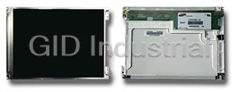
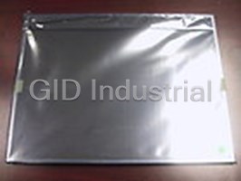
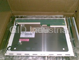
SAMSUNG LTN104S2-L01
Description
Samsung LTN104S2-L01 10.4" TFT 800 x 600 SVGA LCD Panel | LCD Module
Part Number
LTN104S2-L01
Price
Request Quote
Manufacturer
SAMSUNG
Lead Time
Request Quote
Category
LCD CONTROLLERS
Specifications
Display area
211.2(H) x 158.4(V) (10.4? diagonal )
Display colors
262,144
Display Mode
Normally white
Driver element
a-Si TFT active matrix
Number of pixel
800 x 600 (SVGA)
Pixel arrangement
RGB vertical stripe
Pixel pitch
0.264(H) x 0.264(V) (TYP.)
Surface treatment
Haze (25), Hard-Coating 3H
Features
- High contrast ratio, High brightness
- High speed response time
- Low power consumption
- LVDS Interface with 1 pixel / clock (1 channel)
- SVGA (800 x 600 pixels) resolution
- Sync mode (75Hz)
- Thin and light weight
Datasheet

Extracted Text
Product Information ISSUE DATE : 2000-10-21 MODEL : LTN104S2-L01 NOTE : This product information is subject to change after 3 months of issuing date. PREPARED BY : AMLCD Application Engineering Group SAMSUNG ELECTRONICS CO., LTD. Rev.No Doc.No. Page 1 LTN104S2-L01 04-002-G-001021 /25 CONTENTS Revision History - - - - - - - - - - - - - - - - - - - ( 3 ) General Description - - - - - - - - - - - - - - - - - - - ( 4 ) 1. Absolute Maximum Ratings - - - - - - - - - - - - - - - - - - - ( 5 ) 1.1 Absolute Ratings Of Environment 1.2 Electrical Absolute Ratings 2. Optical Characteristics - - - - - - - - - - - - - - - - - - - ( 7 ) 3. Electrical Characteristics - - - - - - - - - - - - - - - - - - - ( 10 ) 3.1 TFT LCD Module 3.2 Back-light Unit 4. Block Diagram - - - - - - - - - - - - - - - - - - - ( 13 ) 4.1 TFT LCD Module 4.2 Back-light Unit 5. Input Terminal Pin Assignment - - - - - - - - - - - - - - - - - - - ( 14 ) 5.1 Input Signal & Power 5.2 LVDS Interface 5.3 Back-light Unit 5.4 Timing Diagrams of LVDS For Transmitting 5.5 Input Signals, Basic Display Colors and Gray Scale of Each Color. 5.6 Pixel format 6. Interface Timing - - - - - - - - - - - - - - - - - - - ( 19 ) 6.1 Timing Parameters 6.2 Input Timing Chart 6.3 Power ON/OFF Sequence 7. Outline Dimension - - - - - - - - - - - - - - - - - - - ( 23 ) 8. General Precautions - - - - - - - - - - - - - - - - - - - ( 24 ) Rev.No Doc.No. Page 2 LTN104S2-L01 04-002-G-001021 /25 Revision History Revision History Date Rev.No. Page Summary Jaue.29.2000 000 Rev.000 was issues. Sep. 01.2000 001 7,10 TBD items are defined. Oct. 07.2000 002 5, 7 Optical characteristics and mechanical spec is changed. ( Wide viewing angle film is applied. ) - Thickness : 6.0 / 6.2 => 6.1 / 6.3 - Weight : 320 / 335g => 330 / 345g - CR : typical 200 => typical 300 - Response time : Tf 20ms => 25ms - Brightness : 220 / 250 => 200 / 230 - Viewing angle : 45/45/20/60 => 60/60/50/50 Rev.No Doc.No. Page 3 LTN104S2-L01 04-002-G-001021 /25 GENERAL DESCRIPTION DESCRIPTION LTN104S2-L01 is a color active matrix TFT (Thin Film Transistor) liquid crystal display (LCD) that uses amorphous silicon TFT as a switching devices. This model is composed of a TFT ″ LCD panel, a driver circuit and a back-light system. The resolution of a 10.4 contains 800 x 600 pixels and can display up to 262,144colors. 6 o'clock direction is the optimum viewing angle. FEATURES Thin and light weight High speed response time High contrast ratio, High brightness SVGA (800 x 600 pixels) resolution Low power consumption Sync mode (75Hz) LVDS Interface with 1 pixel / clock (1 channel) APPLICATIONS Display terminals for AV application products Notebook PC, LCD PC and Web Pad If the usage of this product is not for PC application, but for others, please contact SEC. GENERAL INFORMATION ITEM SPECIFICATION UNIT NOTE ″ Display area 211.2(H) x 158.4(V) (10.4 diagonal ) mm Driver element a-Si TFT active matrix Display colors 262,144 pixel Number of pixel 800 x 600 (SVGA) Pixel arrangement RGB vertical stripe mm Pixel pitch 0.264(H) x 0.264(V) (TYP.) 96dpi Display Mode Normally white Surface treatment Haze (25), Hard-Coating 3H This model doesn’t use Sn plating on the top chassis. Rev.No Doc.No. Page 4 LTN104S2-L01 04-002-G-001021 /25 MECHANICAL INFORMATION ITEM MIN. TYP. MAX. NOTE Horizontal (H) 243.5 244.0 244.5 Module Vertical (V) 171.5 172.0 172.5 size Depth (D) - 6.1 6.3 Weight - 330g 345g 1. ABSOLUTE MAXIMUM RATINGS 1.1 ABSOLUTE RATINGS OF ENVIRONMENT ITEM SYMBOL MIN. MAX. UNIT NOTE T Storage temperature STG (1) -20 60 °C Operating temperature (1) T ° 0 C 50 (Temperature of glass surface) OPR Shock ( non-operating ) (2),(4) Snop - 220 G Vnop - G Vibration (non-operating) 1.5 (3),(4) Note (1) Temperature and relative humidity range are shown in the figure below. ° ≥ 90 % RH Max. ( 40 C Ta) ° ° Maximum wet - bulb temperature at 39 C or less. (Ta > 40%C ) No condensation. Relative Humidity ( %RH) 100 90 80 60 Operating Range 40 20 Storage Range 5 0 -40 -20 0 20 40 60 80 O Temperature ( C) ± ± ± (2) (2)ms, (half) sine wave, one time for X, Y, Z. (3) (10) - (300) Hz, Sweep rate (10) min, (30)min for X,Y,Z. (4) At testing Vibration and Shock, the fixture in holding the Module to be tested have to be hard and rigid enough so that the Module would not be twisted or bent by the fixture. Rev.No Doc.No. Page 5 LTN104S2-L01 04-002-G-001021 /25 1.2 ELECTRICAL ABSOLUTE RATINGS (1) TFT LCD MODULE ( Vss = GND = 0 V) MIN. MAX. UNIT NOTE SYMBOL ITEM ( 1 ) DD Power Supply Voltage V Vss -0.3 4.0 V ( 1 ) DD Logic Input Voltage V Vss -0.3 V +0.3 V IN ± ° NOTE (1) Within Ta = 25 2 C (2) BACK-LIGHT UNIT ± ° Ta = 25 2 C MIN. ITEM SYMBOL MAX. UNIT. NOTE rms Lamp current 2.0 7.0 mA (1) IL Lamp frequency FL (1) 45 80 KHz NOTE (1) Permanent damage to the device may occur if maximum values are exceeded. Functional operation should be restricted to the conditions described under Normal Operating Conditions. Rev.No Doc.No. Page 6 LTN104S2-L01 04-002-G-001021 /25 2. OPTICAL CHARACTERISTICS The following items are measured under stable conditions. The optical characteristics should be measured in a dark room or equivalent state with the methods shown in Note (5). Measuring equipment : TOPCON BM-5A ± ° DD DCLK L * Ta = 25 2 C , V =3.3V, fv= 75Hz, f =49.5MHz, I = 6.0 mA ITEM SYMBOL CONDITION MIN. TYP. MAX. UNIT NOTE Contrast Ratio 200 300 - (1), (2), (5) CR (5 Points) 5 10 - TR Response Rising msec (1), (3) Time at Ta 25 TF - 30 Falling Average Luminance 2 200 230 L,AVE - Y cd/m (1), (4) of White (5 Points) φ = 0, 0.545 0.575 0.605 X R θ = 0 Red RY 0.309 0.339 0.369 Normal Viewing X G 0.283 0.313 0.343 Angle Green Color Y G 0.508 0.538 0.568 Chromaticity ( CIE ) X B 0.122 0.152 0.182 Blue Y B 0.118 0.148 0.178 (1), (5) WX 0.280 0.310 0.340 White WY 0.310 0.340 0.370 50 60 - θ L Hor. θ R Viewing 50 60 - ≥ CR 10 Angle Degrees at center φ H 40 50 - Ver. φ L 40 50 - 13 Points (6) δ L - - 2.0 White Variation Rev.No Doc.No. Page 7 LTN104S2-L01 04-002-G-001021 /25 ≤ Note 1) Definition of Viewing Angle : Viewing angle range(10 C/R) Normal Line φ °, θ ° = 0 = 0 θ L θ R φ H φ L 12 O’clock o θ =90 x y direction L o φ = 90 H y' x' 6 O’clock direction o θ =90 o R φ = 90 L Note 2) Definition of Contrast Ratio (CR) : Ratio of gray max (Gmax) ,gray min (Gmin) at 5 points(4, 5, 7, 9, 10) CR(4) + CR(5) + CR(7) + CR(9) + CR(10) CR = 5 POINTS : 45 , , 7 , 9 , at FIGURE OF NOTE 6) 10 Note 3) Definition of Response time : Display data White(TFT OFF) White(TFT OFF) Black(TFT ON) R T F T % 100 Optical % 90 Response % 10 % 0 Time Note 4) Definition of Average Luminance of White : measure the luminance of white at 5 points. 200 400 600 VIEW AREA Average Luminance of White ( Y L,AVE ) 10 9 150 YL4 + YL5 + YL7 + YL9 + YL10 7 300 Y L,AVE = 5 4 450 5 lines : test point Rev.No Doc.No. Page 8 LTN104S2-L01 04-002-G-001021 /25 Note 5) After stabilizing and leaving the panel alone at a given temperature for 30 minutes, the measurement should be executed. Measurement should be executed in a stable, windless,and dark room. 30 minutes after lighting the back-light. This should be measured in the center of screen. Lamp current : 6.0 mA ± ° Environment condition : Ta = 25 2 C Photo detector ( TOPCON BM-5A) ° Field = 2 40 cm TFT-LCD module LCD panel Center of the screen Optical characteristics measurement setup δ L VER 113 Note 6) Definition of 13 points white variation ( ), CR variation( C ) [ ~ ] Maximum luminance of 13 points δ L = Minimum luminance of 13 points 10mm 10mm 200 400 600 10mm 13 12 11 10 9 150 8 7 6 300 : test point 5 4 450 (lines) 3 2 1 10mm Rev.No Doc.No. Page 9 LTN104S2-L01 04-002-G-001021 /25 3. ELECTRICAL CHARACTERISTICS 3.1 TFT LCD MODULE ± ° Ta = 25 2 C ITEM SYMBOL MIN TYP MAX UNIT NOTE Voltage of Power Supply VDD 3.0 3.3 3.6 V Differential Input VIH - - +100 mV High Voltage for LVDS (1) Receiver Threshold VIL -100 - - mV Low Vsync Frequency fv - 75 - Hz Hsync Frequency fH - 46.875 - KHz Main Frequency fDCLK - 49.5 - MHz Rush Current IRUSH -- 1.5 A (5) White - 270 - mA (2),(4) Current of Mosaic IDD - 280 - mA (2),(4) Power Supply Vertical - 300 330 mA (2),(4) CM Note (1) Condition : V =+1.2V(Common mode Voltage) V DCLK DD (2) f =75Hz, f = 49.5MHZ, V = 3.3V , DC Current. (3) 1 pixel /clock (4) Power dissipation check pattern *a) White Pattern *b)Mosaic Pattern VIEW AREA Display Brightest Gray Level Display Darkest Gray Level Rev.No Doc.No. Page 10 LTN104S2-L01 04-002-G-001021 /25 *c) Vertical stripe pattern G RG B R B RG B RG B R B B RG B RG B R RG B RG B 5) Rush current measurement condition 3.3V M1 2SK1059 VDD ( LCD INPUT) FUSE R1 C1 47K 1uF R2 CONTROL SIGNAL M2 (HIGH to LOW) 2SK1399 1K 12V R3 C2 47K C3 10000pF 1uF VDD rising time is 470us 3.3V DD 0.9V DD 0.1V GND 470us Rev.No Doc.No. Page 11 LTN104S2-L01 04-002-G-001021 /25 3.2 BACKLIGHT UNIT The back-light system is an edge - lighting type with a single CCFT ( Cold Cathode Fluorescent Tube ). The characteristics of a single lamp are shown in the following tables. ± ° Ta=25 2 C ITEM SYMB MIN TYP MAX UNIT NOTE 7.0 L 2.0 6.0 rms Lamp Current I mA (1) - - L 490 rms IL=6mA Lamp Voltage V V L 65 (2) Frequency f 45 80 KHz 2.94 Power Consumption PL-W -(3), IL=6mA Operating Life Time Hr 12,000 20,000 - Hour (4) ° 825 (25 C) Startup Voltage S V - - Vrms (5) 990 (0°C) Note) The waveform of the inverter output voltage must be area symmetric and the design of the inverter must have specifications for the modularized lamp. The performance of the back-light, for example life time or brightness, is much influenced by the characteristics of the DC-AC inverter for the lamp. So all the parameters of an inverter should be carefully designed so as not to produce too much leakage current from high-voltage output of the inverter. When you design or order the inverter, please make sure that a poor lighting caused by the mismatch of the back-light and the inverter(miss lighting, flicker, etc.) never occur. When you confirm it, the module should be operated in the same condition as it is installed in your instrument. Note (1) Lamp current is measured with a high frequency current meter as shown below. HOT : (PINK) 1 COLD : (WHITE) LCD INVERTER 2 A MODULE No 2 Pin is VLOW. (2) Lamp frequency may produce interference with horizontal synchronous frequency and this may cause line flow on the display. Therefore lamp frequency should be detached from the horizontal synchronous frequency and its harmonics as far as possible in order to avoid interference. (3) refer to IL X VL to calculate. (4) Life time (Hr) of a lamp can be defined as the time in which it continues to operate under the ± ° condition Ta = 25 2 C and IL = 7 mArms until one of the following event occurs. 1. When the brightness becomes 50% or lower than it’s original. 2. When the Effective ignition length becomes 80% or lower than it’s original value. (Effective ignition length is defined as an area that has less than 70% brightness compared to the brightness in the center point.) (5) The voltage above this value should be applied to the lamp for more than 1 second to startup Otherwise the lamp may not be turned on. Rev.No Doc.No. Page 12 LTN104S2-L01 04-002-G-001021 /25 4. BLOCK DIAGRAM 4.1 TFT LCD MODULE Connector : DF19L-14P-1H Timing User LVDS Controller Connector DF19L- DS90CF364 14P-1H Source Drive 10.4” SVGA IC TFT-LCD Panel DC-DC Gamma Converter Generator VCOM Generator Video Signal R-String Control Signal Gate VCOM Source/Gate Drive Gamma IC Connector DVDD AVDD Von/Voff 4.2 BACKLIGHT UNIT Reflector 1 HOT (PINK) LAMP 2 COLD(WHITE) Note) The output of the inverter may change according to the material of the reflector. Rev.No Doc.No. Page 13 LTN104S2-L01 04-002-G-001021 /25 5. INPUT TERMINAL PIN ASSIGNMENT 5.1. Input Signal & Power (LVDS, Connector : DF19L-14P-1H : Hirose) PIN NO SYMBOL FUNCTION POLARITY REMARK 1 VDD POWER SUPPLY +3.3V 2 VDD POWER SUPPLY +3.3V 3 GND GROUND 4 GND GROUND RxIN0- LVDS Differential Data INPUT 5 Negative RxIN0+ LVDS Differential Data INPUT 6 Positive RxIN1- LVDS Differential Data INPUT 7 Negative RxIN1+ LVDS Differential Data INPUT 8 Positive RxIN2- LVDS Differential Data INPUT 9 Negative RxIN2+ LVDS Differential Data INPUT 10 Positive RxCLK- LVDS Differential Data INPUT 11 Negative RxCLK+ LVDS Differential Data INPUT 12 Positive GND 13 GROUND GND 14 GROUND Rev.No Doc.No. Page 14 LTN104S2-L01 04-002-G-001021 /25 5.2 LVDS Interface : Transmitter DS90CF363 or Compatible Pin No. Name RGB Signal Pin No. Name RGB Signal 44 TxIN0 RO0 12 TxIN11 GO5 45 TxIN1 RO1 13 TxIN12 BO0 47 TxIN2 RO2 15 TxIN13 BO1 48 TxIN3 RO3 16 TxIN14 BO2 1 TxIN4 RO4 18 TxIN15 BO3 3 TxIN5 RO5 19 TxIN16 BO4 4 TxIN6 GO0 20 TxIN17 BO5 6 TxIN7 GO1 22 TxIN18 Hsync 7 TxIN8 GO2 23 TxIN19 Vsync 9 TxIN9 GO3 25 TxIN20 GND 10 TxIN10 GO4 26 TxCLK IN Clock FPD Link Interface Graphics controller DS90CF364A DF19L-14P-1H DS90CF363 18-bit RED0 44 41 8 TxOUT0- 5 RxIN0- RED1 45 Ω 100 RED2 47 40 9 TxOUT0+ 6 RxIN0+ RED3 48 RED4 1 RED5 3 39 10 TxOUT1- 7 RxIN1- GREEN0 4 Ω 100 6 GREEN1 38 11 TxOUT1+ 8 RxIN1+ 7 GREEN2 9 GREEN3 10 GREEN4 35 14 12 GREEN5 TxOUT2- 9 RxIN2- Ω 100 BLUE0 13 34 15 TxOUT2+ 10 RxIN2+ BLUE1 15 BLUE2 16 BLUE3 18 33 16 TxCLKOUT- 11 RxCLK- BLUE4 19 Ω 100 BLUE5 20 32 17 TxCLKOUT+ 12 RxCLK+ Hsync 22 Vsync 23 Enable 25 CLOCK 26 Note : The LCD Module uses a 100ohm resistor between positive and negative lines of each receiver input. Rev.No Doc.No. Page 15 LTN104S2-L01 04-002-G-001021 /25 5.3 BACK LIGHT UNIT Connector : JST BHSR - 02VS -1 Mating Connector : JST SM02B-BHSS-1 Pin NO. Symbol Color Function 1 HOT PINK High Voltage 2 COLD WHITE Low Voltage 5.4 Timing Diagrams of LVDS for Transmission LVDS Receiver : DS90CF364A or Compatible T TxCLK OUT RxCLK IN T/7 RxOUT20 RxOUT19 RxOUT18 RxOUT17 RxOUT16 RxOUT15 RxOUT14 Rx IN2 GND Vsync Hsync B5 B4 B3 B2 RxOUT13 RxOUT12 RxOUT11 RxOUT10 RxOUT9 RxOUT8 RxOUT7 Rx IN1 B1 B0 G5 G4 G3 G2 G1 RxOUT6 RxOUT5 RxOUT4 RxOUT3 RxOUT2 RxOUT1 RxOUT0 RxIN0 G0 R5 R2 R1 R0 R4 R3 Rev.No Doc.No. Page 16 LTN104S2-L01 04-002-G-001021 /25 5.5 Input Signal,Basic Display Colors and Gray Scale of Each Colors DATA SIGNAL GRAY COLOR DISPLAY SCALE RED GREEN BLUE LEVEL R0 R1 R2 R3 R4 R5 G0 G1 G2 G3 G4 G5 B0 B1 B2 B3 B4 B5 BLACK 0 0 0 0 0 0 0 0 0 0 0 0 0 0 0 0 0 0 - BLUE 0 0 0 0 0 0 0 0 0 0 0 0 1 1 1 1 1 1 - GREEN 0 0 0 0 0 0 1 1 1 1 1 1 0 0 0 0 0 0 - CYAN 0 0 0 0 0 0 1 1 1 1 1 1 1 1 1 1 1 1 - BASIC COLOR RED 1 1 1 1 1 1 0 0 0 0 0 0 0 0 0 0 0 0 - MAGENTA 1 1 1 1 1 1 0 0 0 0 0 0 1 1 1 1 1 1 - YELLOW 1 1 1 1 1 1 1 1 1 1 1 1 0 0 0 0 0 0 - WHITE 1 1 1 1 1 1 1 1 1 1 1 1 1 1 1 1 1 1 - BLACK 0 0 0 0 0 0 0 0 0 0 0 0 0 0 0 0 0 0 R0 1 0 0 0 0 0 0 0 0 0 0 0 0 0 0 0 0 0 R1 DARK 0 1 0 0 0 0 0 0 0 0 0 0 0 0 0 0 0 0 R2 � GRAY : : : : : : : : : : : : : : : : : : SCALE R3~R60 OF : : : : : : : : : : : : : : : : : : � RED 1 0 1 1 1 1 0 0 0 0 0 0 0 0 0 0 0 0 R61 LIGHT 0 1 1 1 1 1 0 0 0 0 0 0 0 0 0 0 0 0 R62 RED 1 1 1 1 1 1 0 0 0 0 0 0 0 0 0 0 0 0 R63 BLACK 0 0 0 0 0 0 0 0 0 0 0 0 0 0 0 0 0 0 G0 0 0 0 0 0 0 1 0 0 0 0 0 0 0 0 0 0 0 G1 DARK 0 0 0 0 0 0 0 1 0 0 0 0 0 0 0 0 0 0 G2 � GRAY : : : : : : : : : : : : : : : : : : SCALE G3~G60 OF : : : : : : : : : : : : : : : : : : � GREEN 0 0 0 0 0 0 1 0 1 1 1 1 0 0 0 0 0 0 G61 LIGHT 0 0 0 0 0 0 0 1 1 1 1 1 0 0 0 0 0 0 G62 GREEN 0 0 0 0 0 0 1 1 1 1 1 1 0 0 0 0 0 0 G63 BLACK 0 0 0 0 0 0 0 0 0 0 0 0 0 0 0 0 0 0 B0 0 0 0 0 0 0 0 0 0 0 0 0 1 0 0 0 0 0 B1 DARK 0 0 0 0 0 0 0 0 0 0 0 0 0 1 0 0 0 0 B2 � GRAY : : : : : : : : : : : : : : : : : : SCALE B3~B60 OF : : : : : : : : : : : : : : : : : : � BLUE 0 0 0 0 0 0 0 0 0 0 0 0 1 0 1 1 1 1 B61 LIGHT 0 0 0 0 0 0 0 0 0 0 0 0 0 1 1 1 1 1 B62 BLUE 0 0 0 0 0 0 0 0 0 0 0 0 1 1 1 1 1 1 B63 Note (1) Definition of Gray : Rn : Red Gray, Gn : Green Gray, Bn : Blue Gray (n = Gray level) (2) Input Signal : 0 = Low level voltage, 1 = High level voltage Rev.No Doc.No. Page 17 LTN104S2-L01 04-002-G-001021 /25 5.6 PIXEL FORMAT Pixel 1 Pixel 800 RG B RG B RG B RG B Line 1 LTN104S2-L01 Panel RG B RG B RG B RG B Line 600 Rev.No Doc.No. Page 18 LTN104S2-L01 04-002-G-001021 /25 6. INTERFACE TIMING 6.1 Timing Parameters SIGNAL ITEM SYMBOL MIN. TYP MAX. UNIT NOTE Clock Frequency 1/TC - 49.5 - MHz Display TVD - 600 - lines Period Vertical Active Display Term Vertical TVB - 25 - lines Blank Period One Line Cycle TH - 1056 - clocks Scanning Time Horizontal Active Display THD - 800 - clocks Display Term Period Rev.No Doc.No. Page 19 LTN104S2-L01 04-002-G-001021 /25 6.2 Input Timing chart Resolution: 800 � 600 at 75 Hz (non-interlaced) Hor Pixels: 800 pixels Ver lines: 600 lines Hor Frequency : 46.875 kHz (21.3 us / line) Ver Frequency : 75 Hz (13.3ms / frame) Pixel clock : 49.5 MHz (20.2 ns) Character Width : 8 Pixels (161.6 ns) HORIZONTAL Sync Polarity : Negative Total time : 21.333 us (1056 pixels) Addressable time : 16.162 us (800 pixels) Blank start : 16.162 us Blank time : 5.172 us (256 pixels) Sync start : 16.485 us (816 pixels) Right border : 0 us Front porch : 0.323 us ( 16 pixels) Sync time : 1.616 us (80 pixels) Back porch : 3.232 us (160 pixels) Left border : 0 us VERTICAL Sync Polarity : Negative Total time : 13.333 ms (625 lines) Addressable time : 12.8 ms (600 lines) Blank start : 12.8 ms (600 lines) Blank time : 0.533 ms (25 lines) Sync start : 12.821 ms ( 601 lines) Bottom border : 0 ms Front porch : 0.021 ms (1 line) Sync time : 0.064 ms (3 lines) Back porch : 0.448 ms ( 21 lines) Top border : 0 ms Definition of Terms Blank time Sync Back Top/Left Addressable Bottom/Right Front Porch Border Video time Border porch Blank Start Sync Start Rev.No Doc.No. Page 20 LTN104S2-L01 04-002-G-001021 /25 Relationship of VSYNC & HSYNC & Display 1 line 3 line VSYNC HSYNC 600 line 1 line Display 21 line Relationship of HSYNC & Clock & Data enable 80 clock HSYNC MCLK Data 16 clock 160 clock 16 clock Enable 800 clock Rev.No Doc.No. Page 21 LTN104S2-L01 04-002-G-001021 /25 6.3 Power ON/OFF Sequence : To prevent a latch-up or DC operation of the LCD module, the power on/off sequence should be as the diagram below. T1 DD 0.9 VDD 0.9 V Power Supply 0.1 VDD VDD 0.1 VDD 0V T4 ��≤�� ≤������� ��≤����≤��������� T2 T3 ��≤����≤��������� �����≤��� Interface Signal VALID 0 V Power On Power Off T5 T6 ���������≤�� ���������≤�� 0.5 VCC 0.5 VCC Power Supply for B/L Unit Power ON/OFF Sequence NOTE. (1) The supply voltage of the external system for the module input should be the same as the definition of VDD. (2) Apply the lamp voltage within the LCD operation range. When the back-light turns on before the LCD operation or the LCD turns off before the back-light turns off, the display may momentarily become white. (3) In case of VDD = off level, please keep the level of input signals on the low or keep a high impedance. (4) T4 should be measured after the module has been fully discharged between power off and on period. (5) Interface signal shall not be kept at high impedance when the power is on. Rev.No Doc.No. Page 22 LTN104S2-L01 04-002-G-001021 /25 7. Outline Dimension Rev.No Doc.No. Page 23 LTN104S2-L01 04-002-G-001021 /25 8. GENERAL PRECAUTIONS 1. Handling (a) When the module is assembled, It should be attached to the system firmly using every mounting holes. Be careful not to twist and bend the modules. (b) Refrain from strong mechanical shock and / or any force to the module. In addition to damage, this may cause improper operation or damage to the module and CCFT back-light. (c) Note that polarizers are very fragile and could be easily damaged. Do not press or scratch the surface harder than a HB pencil lead. (d) Wipe off water droplets or oil immediately. If you leave the droplets for a long time, Staining and discoloration may occur. (e) If the surface of the polarizer is dirty, clean it using some absorbent cotton or soft cloth. (f) The desirable cleaners are water, IPA(Isoprophyl Alcohol) or Hexane. Do not use Ketone type materials(ex. Acetone), Ethyl alcohol, Toluene, Ethyl acid or Methyl chloride. It might permanent damage to the polarizer due to chemical reaction. (g) If the liquid crystal material leaks from the panel, it should be kept away from the eyes or mouth . In case of contact with hands, legs or clothes, it must be washed away thoroughly with soap. (h) Protect the module from static , it may cause damage to the C-MOS Gate Array IC. (i) Use fingerstalls with soft gloves in order to keep display clean during the incoming inspection and assembly process. (j) Do not disassemble the module. (k) Do not pull or fold the lamp wire. (l) Do not adjust the variable resistor which is located on the back side. (m) Protection film for polarizer on the module shall be slowly peeled off just before use so that the electrostatic charge can be minimized. (n) Pins of I/F connector shall not be touched directly with bare hands. Rev.No Doc.No. Page 24 LTN104S2-L01 04-002-G-001021 /25 2. STORAGE (a) Do not leave the module in high temperature, and high humidity for a long time. ° It is highly recommended to store the module with temperature from 0 to 35 C and relative humidity of less than 70%. (b) Do not store the TFT-LCD module in direct sunlight. (c) The module shall be stored in a dark place. It is prohibited to apply sunlight or fluorescent light during the store. 3. OPERATION (a) Do not connect,disconnect the module in the “ Power On” condition. (b) Power supply should always be turned on/off by following item 6.3 “ Power on/off sequence “. (c) Module has high frequency circuits. Sufficient suppression to the electromagnetic interference shall be done by system manufacturers. Grounding and shielding methods may be important to minimize the interference. (d) The cable between the backlight connector and its inverter power supply shall be a minimized length and be connected directly . The longer cable between the backlight and the inverter may cause lower luminance of lamp(CCFT) and may require higher startup voltage(Vs). 4. OTHERS (a) Ultra-violet ray filter is necessary for outdoor operation. (b) Avoid condensation of water. It may result in improper operation or disconnection of electrode. (c) Do not exceed the absolute maximum rating value. ( the supply voltage variation, input voltage variation, variation in part contents and environmental temperature, so on) Otherwise the module may be damaged. (d) If the module displays the same pattern continuously for a long period of time,it can be the situation when the image “sticks” to the screen. (e) This module has its circuitry PCB’s on the rear side and should be handled carefully in order not to be stressed. Rev.No Doc.No. Page 25 LTN104S2-L01 04-002-G-001021 /25
Frequently asked questions
What makes Elite.Parts unique?

What kind of warranty will the LTN104S2-L01 have?
Which carriers does Elite.Parts work with?
Will Elite.Parts sell to me even though I live outside the USA?
I have a preferred payment method. Will Elite.Parts accept it?
Why buy from GID?

Quality
We are industry veterans who take pride in our work

Protection
Avoid the dangers of risky trading in the gray market

Access
Our network of suppliers is ready and at your disposal

Savings
Maintain legacy systems to prevent costly downtime

Speed
Time is of the essence, and we are respectful of yours
Related Products

Samsung LT133X2-122 13.3" TFT 1024 x 768 XGA LCD Module
Samsung LTM150X0-L01 15" TFT 1024 x 768 XGA LCD Module
Request a Quote

The quote request has been received
Close

Facing challenges or have inquiries? Feel free to contact us!
Call Us +1-469-283-2440
What they say about us
FANTASTIC RESOURCE
One of our top priorities is maintaining our business with precision, and we are constantly looking for affiliates that can help us achieve our goal. With the aid of GID Industrial, our obsolete product management has never been more efficient. They have been a great resource to our company, and have quickly become a go-to supplier on our list!
Bucher Emhart Glass
EXCELLENT SERVICE
With our strict fundamentals and high expectations, we were surprised when we came across GID Industrial and their competitive pricing. When we approached them with our issue, they were incredibly confident in being able to provide us with a seamless solution at the best price for us. GID Industrial quickly understood our needs and provided us with excellent service, as well as fully tested product to ensure what we received would be the right fit for our company.
Fuji
HARD TO FIND A BETTER PROVIDER
Our company provides services to aid in the manufacture of technological products, such as semiconductors and flat panel displays, and often searching for distributors of obsolete product we require can waste time and money. Finding GID Industrial proved to be a great asset to our company, with cost effective solutions and superior knowledge on all of their materials, it’d be hard to find a better provider of obsolete or hard to find products.
Applied Materials
CONSISTENTLY DELIVERS QUALITY SOLUTIONS
Over the years, the equipment used in our company becomes discontinued, but they’re still of great use to us and our customers. Once these products are no longer available through the manufacturer, finding a reliable, quick supplier is a necessity, and luckily for us, GID Industrial has provided the most trustworthy, quality solutions to our obsolete component needs.
Nidec Vamco
TERRIFIC RESOURCE
This company has been a terrific help to us (I work for Trican Well Service) in sourcing the Micron Ram Memory we needed for our Siemens computers. Great service! And great pricing! I know when the product is shipping and when it will arrive, all the way through the ordering process.
Trican Well Service
GO TO SOURCE
When I can't find an obsolete part, I first call GID and they'll come up with my parts every time. Great customer service and follow up as well. Scott emails me from time to time to touch base and see if we're having trouble finding something.....which is often with our 25 yr old equipment.
ConAgra Foods