

 Manufacturers
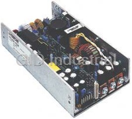
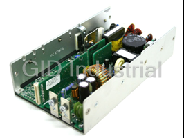
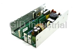
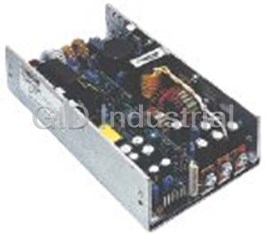
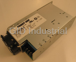
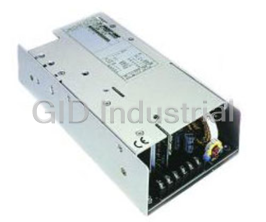
POWER-ONE PSK-1220-7

Description
The PSS/PSK Series of positive switching regulators is
designed as power supplies for electronic systems, where no
input-to-output isolation is required.
Part Number
PSK-1220-7
Price
Request Quote
Manufacturer
POWER-ONE
Lead Time
Request Quote
Category
PRODUCTS - P
Datasheet

Extracted Text
PSS, PSK Series Data Sheet Positive Switching Regulators ® 111 111 4.4" 4.4" 3 U 3 U 80 168 60 3.2" 168 6.6" 2.4" 16 TE 6.6" 12 TE Features Description • Input voltage up to 144 VDC The PSS/PSK Series of positive switching regulators is • Single output of 3.3 to 48 VDC designed as power supplies for electronic systems, where no input-to-output isolation is required. Their major advantages • No input-to-output isolation include a high level of efficiency, high reliability, low output • High efficiency up to 97% ripple, and excellent dynamic response. Models with input • Extremely wide input voltage range voltages up to 144V are specially designed for secondary switched and battery-driven mobile applications. The • Low input-to-output differential voltage converters are suitable for railway applications according to • Very good dynamic properties EN 50155 and EN 50121. • Input undervoltage lockout Two type of housings are available allowing operation up to • Active current sharing for parallel operation 71 °C. They are designed for insertion into a 19" DIN-rack or • Output voltage adjustment, inhibit, and sense lines for chassis mounting. Replacing the heat sink by an optional • Continuously no-load and short-circuit proof cooling plate, allows chassis or wall mounting on top of a metal surface, acting as heat sink. • All boards are coated with a protective lacquer Various options are available to adapt the converter to different applications. Connector type: H15 or H15S4, depending on output current. Table of Contents Page Page Description ............................................................................ 1 Immunity to Environmental Conditions ............................... 13 Model Selection .................................................................... 2 Mechanical Data ................................................................. 14 Functional Description .......................................................... 3 Safety and Installation Instructions ..................................... 16 Electrical Input Data .............................................................. 4 Description of Options ........................................................ 17 Electrical Output Data ........................................................... 6 Accessories......................................................................... 19 Auxiliary Functions .............................................................. 10 EC Declaration of Conformity ............................................. 20 Electromagnetic Compatibility (EMC) ................................. 12 BCD20029-G Rev AA, 28-Apr-09 Page 1 of 20 www.power-one.com PSS, PSK Series Data Sheet Positive Switching Regulators ® Model Selection Table 1: All models 2 Output Output Operating input Nom. input Efficiency Type Connector Options voltage current voltage range voltage designation type η η η η V [V] I [A] V [V] V [V] η η η [%] η η η [%] o nom o nom i i nom min typ 3.3 25 8 – 40 20 81 82 PSK3E25-7 H15S4 -9, E, B, B1, G 5.1 12 8 – 80 40 78 79 PSS5A12-7 H15 -9, E, P, C, B, B1, G 5.1 14 8 – 40 20 83 PSS5A14-2 H15 B, B1 5.1 16 8 – 80 40 78 79 PSK5A16-7 H15 -9, E, P, C, B, B1, G 5.1 18 8 – 40 20 82 PSS5A18-2 H15 B, B1 5.1 20 8 – 80 40 78 79 PSK5A20-9 H15S4 -9, E, P, C, B, B1, G 5.1 25 8 – 40 20 82 82 PSK5A25-9 H15S4 -9, E, P, C, B, B1, G 1 12 9 18 – 144 60 90 91 PSS129-7 H15 -9, E, P, C, B, B1, G 12 12 15 – 80 40 90 91 PSS1212-7 H15 -9, E, P, C, B, B1, G 1 12 12 18 – 144 60 90 91 PSK1212-7 H15 -9, E, P, C, B, B1, G 12 14 15 – 40 30 90 PSS1214-2 H15 B, B1 12 16 15 – 80 40 89 90 PSK1216-7 H15 -9, E, P, C, B, B1, G 12 18 15 – 40 30 90 PSK1218-2 H15 B, B1 12 20 15 – 80 40 89 90 PSK1220-7 H15S4 -9, E, P, C, B, B1, G 3 1 15 9 22 – 144 60 90 92 PSS129-7 H15 -9, E, C, B, B1, G 3 15 12 19 – 80 40 90 92 PSS1212-7 H15 -9, E, C, B, B1, G 3 1 15 12 22 – 144 60 90 92 PSK1212-7 H15 -9, E, C, B, B1, G 3 15 14 19 – 40 30 90 PSS1214-2 H15 B, B1 3 15 16 19 – 80 40 89 90 PSK1216-7 H15 -9, E, C, B, B1, G 3 15 18 19 – 40 30 90 PSK1218-2 H15 B, B1 3 15 20 19 – 80 40 89 90 PSK1220-7 H15S4 -9, E, C, B, B1, G 1 24 9 31 – 144 60 93 94 PSS249-7 H15 -9, E, P, C, B, B1, G 24 12 29 – 80 50 93 94 PSS2412-7 H15 -9, E, P, C, B, B1, G 1 24 12 31 – 144 60 93 94 PSK2412-9 H15 -9, E, P, C, B, B1, G 24 14 29 – 60 40 94 PSS2414-2 H15 B, B1 24 16 29 – 80 50 93 94 PSK2416-9 H15 -9, E, P, C, B, B1, G 24 18 29 – 60 40 90 PSK2418-2 H15 B, B1 24 20 29 – 80 50 93 94 PSK2420-9 H15S4 -9, E, P, C, B, B1, G 1 36 9 44 – 144 80 95 96 PSS369-9 H15 -9, E, P, C, B, B1, G 36 12 42 – 80 60 93 94 PSS249-9 H15 1 36 12 44 – 144 80 95 96 PSK3612-9 H15 36 16 42 – 80 60 94 95 PSK3616-9 H15 36 20 42 – 80 60 94 95 PSK3620-9 H15S4 1 48 9 58 – 144 80 96 97 PSS489-9 H15 1 48 12 58 – 144 80 96 97 PSK4812-9 H15 1 Surges up to 156 V for 2 s; see Electrical Input Data 2 Efficiency at V and I . i nom o nom 3 Output voltage V set to 15 V by R input o 4 Not available for PSK3E25 Note: Non-standard input/output configurations or special custom adaptions are available on request. BCD20029-G Rev AA, 28-Apr-09 Page 2 of 20 www.power-one.com PSS, PSK Series Data Sheet Positive Switching Regulators ® Part Number Description PSK 12 12 -7 E P C B G Positive switching regulator in case S01, K01 ....... PSS, PSK Nominal output voltage in volt.................................... 3.3 – 48 Nominal output current in ampere ................................ 9 – 25 Operational ambient temperature range T A – 10 to 50 °C ..................................................... -2 – 25 to 71 °C ..................................................... -7 – 40 to 71 °C (optional) ..................................... -9 Options: Inrush current limitation ..................................... E 1 Potentiometer to adjust V ............................... P o Thyristor crowbar ............................................... C Cooling plate large/small ............................. B, B1 2 RoHS-compliant for all 6 substances .............. G 1 Option P excludes R-features and vice versa. 2 G is always placed at the end of the part number. Consult Power-One for availability! Example: PSS 129-7EPCB = Positive switching regulator with output 12 V, 9 A, ambient temperature range of –25 to 71 °C, inrush current limitation, potentiometer, crowbar, and large cooling plate option B. Input voltage range, nominal output voltage and current, Product Marking protection degree, batch no., serial no., and data code Type designation, applicable safety approvals and recognition including production site, version (modificationstatus), and marks, warnings, pin allocation, Power-One patents and date of production. company logo. Identification of LED, test sockets, and optional potentiometer. Functional Description back through the freewheeling diode. Regulation is accomplished by varying on/off duty cycle. The switching regulators are using the buck converter topology. The input is not electrically isolated from the output. These regulators are ideal for applications, where an input to output isolation is not necessary or where it is already provided During the on period of the switching FET, current is by an external front end, e.g., a transformer with rectifier. To transferred to the output, and energy is stored in the output choke. During the off period, this energy forces the current to optimize customer’s needs, various options and accessories continue flowing through the output chocke to the load and are available. 03024a I o 4 Fuse Vo+ I i 6 30 + Vi+ C 32 o 20 S+ 22 T C i Control V V 14 i i o circuit Option C 16 R 18 S– 26 Gi– 28 8 Go– 10 24 Option P Fig. 1 + – Block diagram BCD20029-G Rev AA, 28-Apr-09 Page 3 of 20 www.power-one.com Option E Input Filter PSS, PSK Series Data Sheet Positive Switching Regulators ® Electrical Input Data Table 2a: Input data. General Conditions: T = 25 °C, unless T is specified A C Input PSS5A14 PSS1214 PSS2414 Unit PSK5A18 PSK1218 PSK2418 Characteristics Conditions min typ max min typ max min typ max 1 V Operating input voltage I = 0 – I 8 40 15/19 40 29 60 VDC i o o nom T – T C min C max 1 ΔV Min. diff. voltage V – V 2.9 3/4 5 io min i o V Undervoltage lock-out 7.3 7.3 12 i o I No load input current I = 0, V – V 50 50 50 mA i 0 o i min i max V Input RFI level, EN 55011/22 V , I AA A i RFI i nom o nom 0.15 – 30 MHz 1 The second value is valid, if output is set to 15 V with the R-input. Table 2b: Input data. General Conditions: T = 25 °C, unless T is specified A C Input PSK3E25 PSS5A12 PSS1212 Unit PSK5A25 PSK5A16 PSK1216 PSK5A20 PSK1220 Characteristics Conditions min typ max min typ max min typ max 1 V Operating input voltage I = 0 – I 8 40 8 80 15 80 VDC i o o nom T – T C min C max 1 ΔV Min. diff. voltage V – V 4.7/2.9 2.9 3 io min i o V Undervoltage lock-out 6.5 6.5 7.3 i o I No load input current I = 0, V – V 50 50 50 mA i 0 o i min i max I Peak value of inrush current V , with option E 20 40 40 A inr p i nom V Input RFI level, EN 55011/22 V , I BB B i RFI i nom o nom 0.15 – 30 MHz 1 Values for PSK3E25/PSK5A20 Table 2c: Input data. General Conditions: T = 25 °C, unless T is specified A C 1 Input PSS1212 PSS2412 PSS3612 Unit PSK1216 PSK2416 PSK3616 PSK1220 PSK2420 PSK3620 Characteristics Conditions min typ max min typ max min typ max 1 V Operating input voltage I = 0 – I 19 80 29 80 42 80 VDC i o o nom T – T C min C max ΔV Min. diff. voltage V – V 45 6 io min i o V Undervoltage lock-out 7.3 12 19 i o I No load input current I = 0, V – V 50 50 50 mA i 0 o i min i max I Peak value of inrush current V , with option E 40 50 90 A inr p i nom V Input RFI level, EN 55011/22 V , I BB B i RFI i nom o nom 0.15 – 30 MHz 1 Output set to 15 V with the R-input. BCD20029-G Rev AA, 28-Apr-09 Page 4 of 20 www.power-one.com PSS, PSK Series Data Sheet Positive Switching Regulators ® Table 2d: Input data. General Conditions: T = 25 °C, unless T is specified A C 1 Input PSS129 PSS129 PSS249 Unit 1 PSK1212 PSK1212 PSK2412 Characteristics Conditions min typ max min typ max min typ max 2 2 2 V Operating input voltage I = 0 – I 18 144 22 144 31 144 VDC i o o nom T – T C min C max ΔV Min. diff. voltage V – V 67 7 io min i o V Undervoltage lock-out 12 12 24 i o I No load input current I = 0, V – V 50 50 50 mA i 0 o i min i max I Peak value of inrush current V , with option E 4.5 4.5 4.5 A inr p i nom V Input RFI level, EN 55011/22 V , I BB B i RFI i nom o nom 0.15 – 30 MHz 1 Output set to 15 V with the R-input. 2 Surges up to 156 V for 2 s are allowed. Table 2e: Input data. General Conditions: T = 25 °C, unless T is specified A C Input PSS369 PSS488 Unit PSK3612 PSK4812 Characteristics Conditions min typ max min typ max 1 1 V Operating input voltage I = 0 – I 18 144 22 144 VDC i o o nom T – T C min C max ΔV Min. diff. voltage V – V 810 io min i o V Undervoltage lock-out 36 48 i o I No load input current I = 0, V – V 50 50 mA i 0 o i min i max I Peak value of inrush current V , with option E 6 6 A inr p i nom V Input RFI level, EN 55011/22 V , I BB i RFI i nom o nom 0.15 – 30 MHz 1 Surges up to 156 V for 2 s are allowed. characteristic of a switched mode regulator. The input fuse Input Filter and Fuse protects against severe defects. An input filter and a fuse are incorporated in all converters as The maximum permissible additionally superimposed ripple v i standard. The filter reduces emitted electrical noise and of the input voltage (rectifier mode) at a specified input prevents oscillations caused by the negative input impedance frequency f has the following values: i Table 3: Input fuses v = 10 V at 100 Hz, or V = 1000 Hz/f • 1 V i max pp pp i The input fuses are specified in the table 3. Model Fuse type Size Supplier PSK3E25, PSK5A20, PSK5A25 F 25 A 6.3 × 32 mm Littlefuse Inrush Current PSK1220, PSK2420, PSK3620 Depending on the input source and the input impedance, the PSK5A16, PSK1216, PSK1218 F 20 A inrush current into the converter may reach a very high peak PSK2416, PSK2418, PSK3620 value during the switch-on sequence. It also determine the PSS5A12, PSS5A14, F 15 A rating of input devices such as switches, relays, fuses, etc. To PSS1212, PSK1212, PSS1214 protect these input devices by limiting the inrush current, we PSS2412, PSK2412, PSS2414 recommend the choice of the active inrush current limitation PSS3612, PSK3612, PSK3616 circuit, option E. PSK4812 PSS129, PSS249 F 10 A PSS369, PSS489 BCD20029-G Rev AA, 28-Apr-09 Page 5 of 20 www.power-one.com PSS, PSK Series Data Sheet Positive Switching Regulators ® Electrical Output Data General Conditions: • T = 25°C, unless T is specified A C • R control (pin 16) not connected or progammed to V at I o nom o nom • Inhibit input (pin 14) connected to Go– • Sense lines S+ and S– connected at female connector Table 3a: Output data of PSS models 1 Output PSS5A12 PSS1212 PSS1212 Unit Characteristics Conditions min typ max min typ max min typ max V Output voltage V , I 5.07 5.13 11.93 12.07 14.91 15.09 V o i nom o nom I Output current V – V 0120 12 0 12 A o i min i max T – T C min C max I Output current limit 12 15 12 15 12 15 oL v Output Switching freq. V , I 20 40 20 45 30 50 mV o i nom o nom pp voltage IEC/EN 61204 Total incl. spikes 24 44 29 49 34 54 noise BW = 20 MHz ΔV Static line regulation V – V , I 15 35 40 70 50 80 mV o V i min i max o nom ΔV Static load regulation V , I = 0 – I 10 25 30 50 35 55 o l i nom o o nom v Dynamic Voltage deviat. V 70 140 150 o d i nom 1 load I ↔ /3 I o nom o nom t Recovery time 40 60 60 μs d regulation IEC/EN 61204 α Temperature coefficient V – V ±1 ±3 ±4 mV/K Vo i min i max ΔV /ΔT (T to T ) I = 0 – I o C C min C max o o nom ±0.02 ±0.02 ±0.02 %/K 1 Output set to 15 V with R-input. Table 3b: Output data of PSS models. General conditions as per table 3a Output PSS2412 PSS2414 PSS3612 Unit Characteristics Conditions min typ max min typ max min typ max V Output voltage V , I 23.86 24.14 23.2 24.7 35.78 36.22 V o i nom o nom I Output current V – V 0120 14 0 12 A o i min i max T – T C min C max I Output current limit 12 15 14 17.5 12 15 oL v Output Switching freq. V , I 30 60 300 35 60 mV o i nom o nom pp voltage IEC/EN 61204 Total incl. spikes 34 64 310 39 64 noise BW = 20 MHz ΔV Static line regulation V – V , I 80 170 480 120 250 mV o V i min i max o nom ΔV Static load regulation V , I = 0 – I 50 120 240 60 200 o l i nom o o nom v Dynamic Voltage deviat. V 180 700 200 o d i nom 1 I ↔ /3 I load o nom o nom t Recovery time 60 60 70 μs d regulation IEC/EN 61204 α Temperature coefficient V – V ±5 ±5 ±8 mV/K Vo i min i max ΔV /ΔT (T to T ) I = 0 – I o C C min C max o o nom ±0.02 ±0.02 ±0.02 %/K BCD20029-G Rev AA, 28-Apr-09 Page 6 of 20 www.power-one.com PSS, PSK Series Data Sheet Positive Switching Regulators ® Table 3c: Output data of PSS models. General conditions as per table 3a 1 Output PSS129 PSS129 PSS249 Unit Characteristics Conditions min typ max min typ max min typ max V Output voltage V , I 11.93 12.07 14.91 15.09 23.86 24.14 V o i nom o nom I Output current V – V 09 0 9 0 9 A o i min i max T – T C min C max I Output current limit 9 11.25 19 11.25 9 11.25 oL v Output Switching freq. V , I 25 50 20 45 30 50 mV o i nom o nom pp voltage IEC/EN 61204 Total incl. spikes 29 54 34 64 39 65 noise BW = 20 MHz ΔV Static line regulation V – V , I 40 70 50 80 80 170 mV o V i min i max o nom ΔV Static load regulation V , I = 0 – I 30 50 40 60 50 120 o l i nom o o nom v Dynamic Voltage deviat. V 140 140 180 o d i nom 1 load I ↔ /3 I o nom o nom t Recovery time 60 60 60 μs d regulation IEC/EN 61204 α Temperature coefficient V – V ±3 ±4 ±5 mV/K Vo i min i max ΔV /ΔT (T to T ) I = 0 – I o C C min C max o o nom ±0.02 ±0.02 ±0.02 %/K 1 Output set to 15 V with R-input. Table 3d: Output data of PSS models. General conditions as per table 3a Output PSS369 PSS489 Unit Characteristics Conditions min typ max min typ max V Output voltage V , I 35.78 36.22 47.71 48.29V o i nom o nom I Output current V – V 09 0 9 A o i min i max T – T C min C max I Output current limit 9 11.25 9 11.25 oL v Output Switching freq. V , I 35 60 35 60 mV o i nom o nom pp voltage IEC/EN 61204 Total incl. spikes 39 64 39 64 noise BW = 20 MHz ΔV Static line regulation V – V , I 120 250 150 350 mV o V i min i max o nom ΔV Static load regulation V , I = 0 – I 60 120 70 150 o l i nom o o nom v Dynamic Voltage deviat. V 200 200 o d i nom 1 I ↔ /3 I load o nom o nom t Recovery time 70 70 μs d regulation IEC/EN 61204 α Temperature coefficient V – V ±5 ±10 mV/K Vo i min i max ΔV /ΔT (T to T ) I = 0 – I o C C min C max o o nom ±0.02 ±0.02 %/K Table 4a: Output data of PSK models. General conditions as per table 3a Output PSK3E25 PSK5A16 PSK5A20 PSK5A25 Unit Characteristics Conditions min typ max min typ max min typ max min typ max V Output voltage V , I 3.25 3.35 5.07 5.13 5.07 5.13 5.07 5.13 V o i nom o nom I Output current V – V 025 0 160 20 25A o i min i max T – T C min C max I Output current limit 25 31.5 16 20 20 25 25 31.5 oL v Output Switching freq. V , I 20 40 20 40 20 40 20 40 mV o i nom o nom pp voltage IEC/EN 61204 Total incl. spikes 24 44 24 44 24 44 24 44 noise BW = 20 MHz ΔV Static line regulation V – V , I 15 35 15 35 15 35 15 35 mV o V i min i max o nom Static load regulation V , I = 0 – I 10 25 10 25 10 25 10 25 ΔV o l i nom o o nom v Dynamic Voltage deviat. V 70 70 70 70 o d i nom 1 I ↔ /3 I load o nom o nom t Recovery time 40 40 40 40 μs d regulation IEC/EN 61204 α Temperature coefficient V – V ±1 ±1 ±1 ±1 mV/K Vo i min i max ΔV /ΔT (T to T ) I = 0 – I o C C min C max o o nom ±0.02 ±0.02 ±0.02 ±0.02 %/K BCD20029-G Rev AA, 28-Apr-09 Page 7 of 20 www.power-one.com PSS, PSK Series Data Sheet Positive Switching Regulators ® Table 4b: Output data of PSK models. General conditions as per table 3a 1 1 Output PSK1216 PSK1220 PSK1216 PSK1220 Unit Characteristics Conditions min typ max min typ max min typ max min typ max V Output voltage V , I 11.93 12.07 11.93 12.07 14.91 15.09 14.91 15.09 V o i nom o nom I Output current V – V 016 0 200 16 20A o i min i max T – T C min C max I Output current limit 16 20 20 25 16 20 20 25 oL v Output Switching freq. V , I 25 45 25 45 30 50 30 50 mV o i nom o nom pp voltage IEC/EN 61204 Total incl. spikes 29 49 29 49 34 54 34 54 noise BW = 20 MHz ΔV Static line regulation V – V , I 40 70 40 70 50 80 50 80 mV o V i min i max o nom ΔV Static load regulation V , I = 0 – I 30 50 30 50 35 55 30 55 o l i nom o o nom v Dynamic Voltage deviat. V 140 140 150 150 o d i nom 1 load I ↔ /3 I o nom o nom t Recovery time 60 60 60 60 μs d regulation IEC/EN 61204 α Temperature coefficient V – V ±3 ±3 ±4 ±4 mV/K Vo i min i max ΔV /ΔT (T to T ) I = 0 – I o C C min C max o o nom ±0.02 ±0.02 ±0.02 ±0.02 %/K 1 Output set to 15 V with R-input. Table 4c: Output data of PSK models. General conditions as per table 3a Output PSK2416 PSK2420 PSK3616 PSK3620 Unit Characteristics Conditions min typ max min typ max min typ max min typ max V Output voltage V , I 23.88 24.14 23.86 24.14 35.78 36.22 35.78 36.22 V o i nom o nom I Output current V – V 016 0 200 16 20A o i min i max T – T C min C max I Output current limit 16 20 20 25 16 20 20 25 oL v Output Switching freq. V , I 30 60 30 60 35 60 35 60 mV o i nom o nom pp voltage IEC/EN 61204 Total incl. spikes 34 64 34 64 39 64 39 64 noise BW = 20 MHz ΔV Static line regulation V – V , I 80 170 80 170 120 250 120 250 mV o V i min i max o nom ΔV Static load regulation V , I = 0 – I 50 120 50 120 60 200 60 200 o l i nom o o nom v Dynamic Voltage deviat. V 180 180 200 200 o d i nom 1 I ↔ /3 I load o nom o nom t Recovery time 60 60 70 70 μs d regulation IEC/EN 61204 α Temperature coefficient V – V ±5 ±5 ±8 ±8 mV/K Vo i min i max ΔV /ΔT (T to T ) I = 0 – I o C C min C max o o nom ±0.02 ±0.02 ±0.02 ±0.02 %/K Table 4d: Output data of PSK models. General conditions as per table 3a 1 Output PSK1212 PSK1212 PSK2424 Unit Characteristics Conditions min typ max min typ max min typ max V Output voltage V , I 11.93 12.07 14.91 15.09 23.86 24.14 V o i nom o nom I Output current V – V 0120 12 0 12 A o i min i max T – T C min C max I Output current limit 12 15 12 15 12 15 oL v Output Switching freq. V , I 25 50 30 60 35 60 mV o i nom o nom pp voltage IEC/EN 61204 Total incl. spikes 29 54 34 64 39 65 noise BW = 20 MHz ΔV Static line regulation V – V , I 40 70 50 80 80 170 mV o V i min i max o nom ΔV Static load regulation V , I = 0 – I 30 50 40 60 50 120 o l i nom o o nom v Dynamic Voltage deviat. V 140 140 180 o d i nom 1 load I ↔ /3 I o nom o nom t Recovery time 60 60 60 μs d regulation IEC/EN 61204 α Temperature coefficient V – V ±3 ±4 ±5 mV/K Vo i min i max ΔV /ΔT (T to T ) I = 0 – I o C C min C max o o nom ±0.02 ±0.02 ±0.02 %/K 1 Output set to 15 V with R-input BCD20029-G Rev AA, 28-Apr-09 Page 8 of 20 www.power-one.com PSS, PSK Series Data Sheet Positive Switching Regulators ® Table 4e: Output data of PSK models. General conditions as per table 3a Output PSK3612 PSK4812 Unit Characteristics Conditions min typ max min typ max V Output voltage V , I 35.78 36.22 47.71 48.29V o i nom o nom I Output current V – V 012012 A o i min i max T – T C min C max I Output current limit 12 15 12 15 oL v Output Switching freq. V , I 35 60 35 60 mV o i nom o nom pp voltage IEC/EN 61204 Total incl. spikes 39 64 39 64 noise BW = 20 MHz ΔV Static line regulation V – V , I 120 250 150 350 mV o V i min i max o nom ΔV Static load regulation V , I = 0 – I 60 120 70 150 o l i nom o o nom v Dynamic Voltage deviat. V 200 200 o d i nom 1 I ↔ /3 I load o nom o nom t Recovery time 70 70 μs d regulation IEC/EN 61204 α Temperature coefficient V – V ±5 ±10 mV/K Vo i min i max ΔV /ΔT (T to T ) I = 0 – I o C C min C max o o nom ±0.02 ±0.02 %/K Output Voltage Regulation V /V The dynamic load regulation is shown in fig. 2 o o nom 05038a V 1.0 o V od V ±1% V ±1% o o 0.8 I o L 0.6 V od 0.4 t t d d 0.2 t 0 0.2 0.4 0.6 0.8 1.0 1.2 I /I I /I o o nom o o nom 1 Fig. 3 Overload, short-circuit behaviour V versus I . o o 0.5 ≥ 10 µs ≥ 10 µs 0 t 05102c Parallel and Series Connection Fig. 2 Outputs of equal nominal voltage may be parallel-connected. Interconnect the current sharing pins T (pin 22) for even Dynamic load regulation. distribution of the output current; see Auxiliary Functions. Output Protection Outputs can be series-connected with any other regulator, provided that the regulators are powered by electrically A voltage suppressor diode, which in worst case conditions isolated source voltages. In series connection the maximum fails into a short-circuit, protects the output against an output current is limited by the lowest current limitation. internally generated overvoltage. Such an overvoltage could occur due to a failure of either the control circuit or the switching transistor. The output protection is not designed to withstand externally applied overvoltages. Current Limitation A constant current limitation circuit holds the output current I o almost constant in the area of 100 to 120% of I , when an o nom overload or a short-circuit is applied to the output. It acts self- protecting and recovers – in contrary to the fold back method – automatically after removal of the overload or short-circuit condition. BCD20029-G Rev AA, 28-Apr-09 Page 9 of 20 www.power-one.com PSS, PSK Series Data Sheet Positive Switching Regulators ® Thermal Considerations and Protection sink, forced cooling, etc.) are taken to ensure that the case temperature T does not exceed its maximum value. C When a switching regulator is located in free, quasi-stationary The regulater is protected by an internal temperature sensor, air (convection cooling) at a temperature T and is operated A max which inhibits the output above T . The output at its nominal output current I , the case temperature T C max o nom C automatically recovers, when the temperature drops below can rise over T after the warm-up phase. T is measured C max C T . at the measuring point of case temperature; see Mechanical C max Data. Under practical operating conditions, the ambient temperature I /I o o nom T may exceed T , provided that additional measures (heat A A max 05031a 1.0 I /I o o nom 0.9 forced 05032a 0.8 cooling 1.0 convection cooling 0.7 0.9 T C max 0.6 0.8 forced 0.5 cooling 0.7 convection cooling 0.4 0.6 0.3 T C max 0.5 0.2 0.4 0.1 0.3 T 0 A 0.2 T 50 60 70 80 90 °C A min 0.1 T 0 A T 40 50 60 70 80 °C A min Fig. 4b Fig. 4a Output current derating versus temperature (models -7 or -9). Output current derating versus temperature (models -2) I [mA] Auxiliary Functions inh 06034a 5 Inhibit (Remote On / Off) 4 The inhibit input allows to enable or disable the output with a control signal. In systems with several regulations, this feature 3 can be used to control the activation sequence of the regulators by a logic signal (TTL, C-MOS, etc.). An output 2 Output on Output off voltage overshoot will not occur, when switching on or off. 1 The inhibit signal is referenced to the S– (pin 18). The signal i 0 and the switching times are specified in table 5, fig. 5, and fig. V inh –40 –20 0 20 40 V 6. Fig. 5 Note: With open i input, the output is enabled. Specification of the inhibit signal (typical) V /V o o nom Table 5: Inhibit characteristics 06001 1 Characteristics Conditions min typ max Unit V Inhibit input voltage V = on V – V –50 +0.8 V inh o i min i max 0.1 t 0 T –T C min C max V = off +2.4 +50 t t o r f t Switch-on time V = V 130 ms r i i nom Inhibit R =V /I L o nom o nom t Switch-off time 25 1 f I Input current when inhibited V = V 25 mA 0 t i inh i i nom Fig. 6 Output response as a function of the inhibit signal BCD20029-G Rev AA, 28-Apr-09 Page 10 of 20 www.power-one.com V = 0.8 V inh V = 2.4 V inh PSS, PSK Series Data Sheet Positive Switching Regulators ® 06049a Sense Lines Vi+ S+ This feature enables compensation of the voltage drop across 20 the connector contacts and the load lines. If the sense lines are R ext2 4 kΩ connected at the load rather than directly at the connector, the V = 2.5 V ref 16 user must ensure that V (between Vo+ and Go–) is not R o max + exceeded. Control V R ext ext1 logic Applying generously dimensioned cross-section load leads - reduces the voltage drop. To minimize noise pick-up, the Vi– S– 18 sense lines should be wired in parallel or twisted. To ensure correct operation, both sense lines must be Fig. 8 connected to their respective power output. The voltage Voltage adjustment via R-input difference between any sense line and its respective power output pin (as measured on the connector) should not exceed the values given in table 4. R Control (Output Voltage Adjust) Note: Sense lines should always be connected! It is Note: With open R input, V ≈ V . o o nom recommended to connect the sense lines directly at the female The output voltage V can either be adjusted with an external connector. o voltage source (V ) or with an external resistor (R or R ). The ext 1 2 adjustment range is 0 – V . The minimum differential o max Table 6: Allowed voltage compensation using sense lines voltage ΔV between input and output (see Electrical Input io min Data) should be maintained. Nominal output Total voltage difference Voltage difference voltage between both sense lines between a) V = 0 – V , using V between R and S–: o o max ext and their respective output Go– and S– V V o ext ––––– ––––– V ≈ 2.5 V • V ≈ V • ext o o nom 3.3 V, 5.1 V ≤0.5 V ≤0.25 V V 2.5 V o nom Caution: To prevent damage V should not exceed 20 V, nor be ext 12 – 48 V ≤1.0 V ≤0.25 V negative. b) V = 0 to V , using R between R and S–: o o nom 1 06046a 4000 Ω • V V • R o o nom 1 ––––––––––– ––––––––––– R ≈ V ≈ 1 o Vi+ V – V R + 4000 Ω o nom o 1 Vo+ i S+ c) V = V to V , using R between R and S+: o o nom o max 2 Load R 4000 Ω • V • (V – 2.5 V) o o nom S– – ––– ––––––––––––––––––––––––––––– R ≈ T 2 2.5 V • (Vo – Vo nom) Go– Gi– V • 2.5 V • R o nom 2 – ––– –––––––––––––––––––––––––––––––––––– V ≈ o 2.5 V • (R + 4000 Ω) – V • 4000 Ω 2 o nom Fig. 7 Caution: To prevent damage, R should never be less than 47 2 Sense lines connection kΩ. Current Sharing Test Sockets For parallel operation of several regulators, interconnect all T- Test sockets (pin ∅ = 2 mm) for measuring the output voltage pins to ensure that the output currents are evenly distributed. V at the sense lines, are located at the front side of the This feature improves transient load performance and o regulator. The test sockets are protected by a series resistor. increases system reliability. All paralleled regulators should be supplied by equal input voltage (V). The output lines should i LED Output Voltage Indicator exhibit equal length and cross section to provide equal voltage drop. A green indicator LED illuminates, when the output voltage is present. Table 7: Maximum adjustable output voltage V Nominal Output Volt. Conditions 3.3 V 5.1 V 12/15 V 24 V 36 V 48 V Unit o nom min typ min typ min typ min typ min typ min typ V Maximum adjustable V , I ?? 5.6 16 26 42.5 52.8 V o max i nom o nom output voltage with R-input BCD20029-G Rev AA, 28-Apr-09 Page 11 of 20 www.power-one.com PSS, PSK Series Data Sheet Positive Switching Regulators ® Electromagnetic Compatibility (EMC) Electromagnetic Immunity General condition: Case not earthed. Table 8: Immunity type tests Phenomenon Standard Class Coupling Value Waveform Source Test In Per- 1 4 Level mode applied imped. procedure oper. form. 2 2 Direct transients IEC 60571-1 i/c, +i/–i 800 V 100 μs 100 Ω yes B p 1500 V 50 μs 1 pos. and 1 neg. p voltage surge per coupling mode 3000 V 5 μs p 4000 V 1 μs p 7000 V 100 ns p 2 2 Electrostatic IEC/EN 4 contact discharge 8000 V 1/50 ns 330 Ω 10 positive and yes A p 3 3 discharge 61000-4-2 3 to case 6000 V 10 negative p discharges 2 2 Electromagnetic IEC/EN 3 antenna 10 V/m AM 80% 80 – 1000 MHz yes A 3 3 field 61000-4-3 2 3 V/m 1 kHz 2 2 Electrical fast IEC/EN 3 i/c, +i/–i 2000 V bursts of 5/50 ns 50 Ω 60 s positive yes A p 3 3 transients/burst 61000-4-4 2 1000 V 5 kHz rep. rate 60 s negative p transients with transients per 2 2 5 4 4000 V B p 15 ms burst coupling mode 3 3 3 2000 V p duration and 300 ms period 2 2 Surges IEC/EN 3 i/c 2000 V 1.2/50 μs 12 Ω 5 pos. and 5 neg. yes A p 3 3 61000-4-5 2 1000 V surges per p coupling mode 2 2 3 +i/–i 2000 V 1.2/50 μs 12 Ω p 3 3 2 500 V p 2 2 Conducted IEC/EN 3 i, o, signal wires 10 VAC AM 80% 150 Ω 0.15 – 80 MHz yes A 3 3 disturbances 61000-4-6 2 3 VAC 1 kHz 1 i = input, o = output, c = case 2 Not applicable for -2 models 3 Valid for -2 models 4 A = Normal operation, no deviation from specifications, B = Normal operation, temporary loss of function or deviation from specs possible 5 With option C, manual reset might be necessary. Electromagnetic Emissions dBμV 07022a 80 EN 55022 A EN 55022 B 60 40 20 Fig. 9 Typical disturbance voltage (quasi-peak) at the input according to EN 55011/22 0 MHz measured at V and I . i nom o nom BCD20029-G Rev AA, 28-Apr-09 Page 12 of 20 www.power-one.com 0.02 0.05 0.1 0.5 1 2 5 10 20 30 PSS, PSK Series Data Sheet Positive Switching Regulators ® Immunity to Environmental Conditions Table 9: Mechanical and climatic stress Test Method Standard Test Conditions Status ±2 Cab Damp heat IEC/EN 60068-2-78 Temperature: 40 °C Regulator +2/-3 steady state MIL-STD-810D section 507.2 Relative humidity: 93 % not Duration: 56 days operating 2 Ea Shock IEC/EN 60068-2-27 Acceleration amplitude: 50 g = 490 m/s Regulator n (half-sinusoidal) MIL-STD-810D section 516.3 Bump duration: 11 ms operating Number of bumps: 18 (3 each direction) 2 Eb Bump IEC/EN 60068-2-29 Acceleration amplitude: 25 g = 245 m/s Regulator n (half-sinusoidal) MIL-STD-810D section 516.3 Bump duration: 11 ms operating Number of bumps: 6000 (1000 each direction) Fc Vibration IEC/EN 60068-2-6 Acceleration amplitude: 0.35 mm (10 – 60 Hz) Regulator 2 (sinusoidal) MIL-STD-810D section 514.3 5 g = 49 m/s (60 – 2000 Hz) operating n Frequency (1 Oct/min): 10 – 2000 Hz Test duration: 7.5 h (2.5 h each axis) 2 Fda Random vibration IEC/EN 60068-2-35 Acceleration spectra density: l 0.05 g /Hz Regulator wide band DIN 40046 part 23 Frequency band: 20 – 500 Hz operating Reproducibility Acceleration magnitude: 4.9 g n rms high Test duration: 3 h (1 h each axis) Kb Salt mist, cyclic IEC/EN 60068-2-52 Concentration: 5% (30 °C) Regulator (sodium chloride Duration: 2 h per cycle not NaCl solution) Storage: 40 °C, 93% rel. humidity operating Storage duration: 22 h per cycle Number of cycles: 3 Temperatures Table 10: Temperature specifications, valid for an air pressure of 800 - 1200 hPa (800 - 1200 mbar) Temperature -2 -7 -9 (Option) Characteristics Conditions min max min max min max Unit 1 T Ambient temperature Regulator –10 50 –25 71 –40 71 °C A operating T Case temperature –10 80 –25 95 –40 95 C 1 T Storage temperature Non operational –25 100 –40 100 –55 100 S 1 See Thermal Considerations and Overtemperature Protection. Reliability Table 11: MTBF and device hours 1 MTBF Ground Benign Ground Fixed Ground Mobile Device Hours MTBF acc. to MIL-HDBK-217F T = 40 °C T = 40 °C T = 70 °C T = 50 °C C C C C 335 000 h 138 000 h 35 000 h 33 000 h 2 100 000 h 1 Statistical values, based on an average of 4300 working hours per year and in general field use BCD20029-G Rev AA, 28-Apr-09 Page 13 of 20 www.power-one.com PSS, PSK Series Data Sheet Positive Switching Regulators ® Mechanical Data PSS Models European The regulators are designed to be inserted into a rack Projection according to IEC 60297-3. Dimensions in mm. 7 TE 5 TE 30.3 3.27 7.04 171.9 10.34 76 50 8 4 x M4 LED OK green Potentiometer (option P) + Test sockets – Measuring point of case temperature T C 27.38 Back plate Front plate Main face d 60 ±0.5 168.5 ∅5 x 90° ∅2.8 Screw holes of the frontplate Fig. 10 Case S01 for PSS models; weight 1.3 kg Aluminium, fully enclosed, black finish EP power-coated, and self cooling. Notes: – d ≥15 mm, recommended minimum distance to next part to ensure proper air circulation at full output power. – Free air locations: the regulator should be mounted with its fins in vertical position to achieve a maximum air flow through heat sink. BCD20029-G Rev AA, 28-Apr-09 Page 14 of 20 www.power-one.com 25.9 11.8 5 50.5 ±0.5 111 103 30.5 51.5 17.8 13.3 7.8 0.2 09028a PSS, PSK Series Data Sheet Positive Switching Regulators ® PSK Models The regulators are designed to be inserted into a rack European Projection according to IEC 60297-3. Dimensions in mm. 7 TE 9 TE 30.3 3.27 7.04 159 4.5 10.34 LED OK green Potentiometer (option P) + Test sockets – Measuring point of case temperature T C 50 27.38 171.9 80 d Back plate Main face Front plate 168.5 ∅5 x 90° ∅2.8 Screw holes of the frontplate Fig. 11 Case K01 for PSK models, weight 1.6 kg Aluminium, fully enclosed, black finish EP power-coated, and self cooling. Notes: – d ≥15 mm, recommended minimum distance to next part to ensure proper air circulation at full output power. – Free air locations: the regulator should be mounted with its fins in vertical position to achieve a maximum air flow through heat sink. BCD20029-G Rev AA, 28-Apr-09 Page 15 of 20 www.power-one.com 89 25.9 11.8 6.5 ±0.5 111 103 51.5 30.5 17.8 13.3 7.8 0.2 09029a PSS, PSK Series Data Sheet Positive Switching Regulators ® Installation Instruction Safety and Installation Instructions Installation of the regulators must strictly follow the national Connector Pin Allocation safety regulations in compliance with the enclosure, mounting, creepage, clearance, casualty, markings, and segregation The connector pin allocation table defines the electrical requirements of the end-use application. potentials and the physical pin positions on the H15 or H15S4 connector. Pin 24 (protective earth) is a leading pin, which The input and the output circuit are not separated. The provides electrical contact first. The regulators should only be negative path is internally interconnected. wired via the female connector H15 (according to DIN 41612) The regulators should be connected to a secondary circuit. to ensure requested safety! Make sure that a regulator failure (e.g. by an internal short- circuit) does not result in a hazardous condition. 10010a Do not open the regulator! Fixtures for connector retention clips V Standards and Approvals (see Accessories) All switching regulators are class-I equipments and have been approved according to UL 60950, CSA 60950, and IEC/EN 60950. The regulators have been evaluated for: 32 4 • Building in Type H15 • Operational insulation from input to output and input/output to case • The use in a pollution degree 2 environment Fixtures for connector retention clips V • Connecting the input to a secondary circuit, which is subject (see Accessories) to a maximum transient rating of 1500 V. The switching regulators are subject to manufacturing surveillance in accordance with the above mentioned standards and with ISO 9001:2000. 30/32 4/6 Type H15S4 Cleaning Agents Fig. 12 In order to avoid possible damage, any penetration of cleaning View of H15 and H15S4 male connector fluids must be prevented, since the regulators are not hermetically sealed. Table 12: H15 and H15S4 connector pin allocation Protection Degree Electrical Determination Type H15 Type H15S4 The protection degree is IP 30 (IP 20, if equipped with option P). It applies only, if the regulator is plugged-in or Pin no. Ident. Pin no. Ident. the matching female connector is properly attached. Output voltage (positive) 4 Vo+ 4/6 Vo+ Output voltage (positive) 6 Vo+ Isolation and Protective Earth Output voltage (negative) 8 Go– The resistance of the protective earth connection (max. 8/10 Go– Output voltage (negative) 10 Go– 0.1 Ω) is tested. Also the electric strength between the input interconnected with the output and the case is Crowbar trigger input (option C) 12 C 12 C tested with 500 VDC (all -2 models), 750 VDC (models Inhibit input 14 i 14 i with V = 80 V), or 1500 VDC (models with V = i max i max 1 1 1 R-input (output voltage programming) 16 R 16 R 144), ≥1 s. Sense line (negative) 18 S– 18 S– These tests are performed in the factory as routine test Sense line (positive) 20 S+ 20 S+ in accordance with EN 50116 and IEC/EN 60950. The Current sharing control input 22 T 22 T electric strength test should not be repeated by the customer. Power-One will not honor any warranty Protective ground (leading pin) 24 24 claims resulting from electric strength tests. Input voltage (negative) 26 Gi– 26/28 Gi– Input voltage (negative) 28 Gi– Railway Application Input voltage (positive) 30 Vi+ The regulators have been developed observing the 30/32 Vi+ Input voltage (positive) 32 Vi+ railway standards EN 50155 and EN 50121. All boards are coated with a protective lacquer. 1 Not available with option P BCD20029-G Rev AA, 28-Apr-09 Page 16 of 20 www.power-one.com PSS, PSK Series Data Sheet Positive Switching Regulators ® Î [A] 11029a Description of Options -9 Extended Temperature Range Inrush limit Soft start Normal operation (R bypassed) s This option defines an extended temperature range as V i (I = ––––) i specified in table 10. R s P Potentiometer to Adjust the Output Note: Option P is not recommended, if several regulators are operated in parallel connection. t 0 40 (typical) 100 (typical) ms Option P excludes R function; the R-input (pin 16) should be left open-circuit. The output voltage V can be adjusted in the o Fig. 13 range 90 - 110% of V . o nom Option E: Inrush current versus time. R is the startup resistor s However, the minimum differential voltage V between input i max (R = 1 Ω for models with V ≤ 80 V, R = 15 Ω for models s i max s and output as specified in Electrical Input Data should be with V > 80 V) i max maintained. E Inrush Current Limitation Depending on the application, further decentralized Note: This option requires an increased minimum input voltage overvoltage protection elements may have to be used V of up to 1 V, dependent upon input range. i max additionally. In regulators without option E, after application of the input A fixed-value monitoring circuit checks the output voltage V , o supply the inrush current is limited by parasitic components of and when the trigger voltage V is reached, the thyristor o c the voltage source and the regulator input only. The regulator crowbar triggers and disables the output. input exhibits a very low impedance, and when driven from a low impedance source, for example a battery, the inrush An external connection C (crowbar trigger control) is provided. When crowbar option is used with two or more power supplies current can peak at several orders of magnitude above the continuous input current. in parallel connection, all crowbar trigger terminals (C) should be interconnected. This ensures all crowbar circuits triggering Option E dramatically reduces this peak current and is simultaneously, in order to disable all outputs at once. The recommended for any application to protect series elements crowbar trigger voltage is maintained between Vo+ and Go–. such as fuses, switches, or circuit brakers. The startup circuit is To prevent false triggering, the user should ensure that V o bypassed during normal operation. (between Vo+ and Go–) deos not exceed V . o c C Thyristor Crowbar G RoHS Compliance Note: The crowbar can be reset by removal of the input voltage Models with G are RoHS-compliant for all six substances. only. The inhibit signal cannot deactivate the thyristor. Option C protects the load against power supply malfunction. It is not designed to sink external currents. As a central overvoltage protection device, the crowbar is usually connected to the external load via distributed inductance of the lines. For this reason, the overvoltage at the load can temporarily exceed the trigger voltage V . o c Table 13: Crowbar trigger levels Characteristics Conditions PSS5A12 PSS129 PSS249 PSS369 PSS 489 Unit PSK5A16 PSS1212 PSS2412 PSS3612 PSK 4812 PSK5A20 PSK1212 PSK2412 PSK3612 PSK5A25 PSK1216 PSK2416 PSK3616 PSK1220 PSK2420 PSK3620 min typ max min typ max min typ max min typ max min typ max V Trigger voltage T – T 6.3 6.7 17.8 18.9 28.89 30.6 47 50 63 67 V o c C min C max 1 1 1 1 V – V 14.3 15.2 43 45.5 i min i max I = 0 – I o o nom t Delay time 1.5 1.5 1.5 1.5 1.5 μs s 1 Models with option P BCD20029-G Rev AA, 28-Apr-09 Page 17 of 20 www.power-one.com PSS, PSK Series Data Sheet Positive Switching Regulators ® to guarantee that the maximum case temperature T is not B, B1 Cooling Plate C max exceeded. The required cooling capacity can be calculated by Where a cooling surface is available, a cooling plate (option B the following formula: or option B1) can be fitted instead of the standard heatsink. 100% – η The mounting system must ensure sufficient cooling capacity P = –––––––- • (V • I ) Loss o o η 5 47.2 6.5 11027 38.5 European 11.8 Projection ±0.2 17.3 133.4 30 168 Fig. 14 Option B, large cooling plate Weight: 1.3 kg 5 47.2 38.5 5 158 11.8 11028 M 4 ±0.5 168 171.9 Fig. 15 Option B1, small cooling plate Weight: 1.2 kg BCD20029-G Rev AA, 28-Apr-09 Page 18 of 20 www.power-one.com 140 111 127 6.5 101 5 13 11.2 PSS, PSK Series Data Sheet Positive Switching Regulators ® Accessories A variety of electrical and mechanical accessories are available including: • Various mating connectors H15 and H15S4 including fast- on, screw, solder or press-fit terminals, code key system and coding clips [HZZ00202] • Connector retention brackets CRB [HZZ01216] • Connector retention clips V [HZZ01209] • Cable connector housing (cable hood) KSG-H15/H15S4 [HZZ00141], also available with fixation [HZZ00142] DIN-rail mounting assembly DMB-K/S • Various front panels for 19" racks with 3U heigth, 12 or 16 TE, Schroff or Intermas • Wall-mounting plate K02 [HZZ01213] for models with option B1 • Brackets for DIN-rail and wall mounting [HZZ00610] • DIN-rail mounting assembly DMB-K/S [HZZ0615] • Additional external input and output filters • Battery sensor [S-KSMH...] for using the converter as a battery charger. Different cell characteristics can be Wall-mounting plate selected; see Battery Charging/Temperature Sensor MOUNTINGPLATE-K02 For additional accessory product information, see the accessory data sheets listed with each product series or individual model listing at www.power-one.com. H15 female connector, code key system 20 to 30 Ncm Front panels Connector Connector retention retention clip V brackets CRB NUCLEAR AND MEDICAL APPLICATIONS - Power-One products are not designed, intended for use in, or authorized for use as critical components in life support systems, equipment used in hazardous environments, or nuclear control systems without the express written consent of the respective divisional president of Power-One, Inc. TECHNICAL REVISIONS - The appearance of products, including safety agency certifications pictured on labels, may change depending on the date manufactured. Specifications are subject to change without notice. BCD20029-G Rev AA, 28-Apr-09 Page 19 of 20 www.power-one.com PSS, PSK Series Data Sheet Positive Switching Regulators ® EC Declaration of Conformity We Power-One AG Ackerstrasse 56 CH-8610 Uster declare under our sole responsibility that all PSx Series switching regulators carrying the CE-mark are in conformity with the provisions of the Low Voltage Directive (LVD) 2006/95/ EC of the European Communities.. Conformity with the directive is presumed by conformity wih the following harmonized standards: • EN 61204: 1995 (= IEC 61204: 1993, modified) Low-voltage power supply devices, DC output - Perfomance characteristics and safety requirements • EN 60950: 1992 + A1: 1993 + A2 (= IEC 950 second edition 1991 + A1: 1992 + A2: 1993) - Safety of information technology equipment The installation instructions given in the corresponding data sheet describe correct installation leading to the presumption of conformity of the end product with the LVD. All PSx Series Switching Regulators are components, intended exclusively for inclusion within other equipment by an industrial assembly operation or by professional installers. They must not be operated as stand alone products. Hence conformity with the Electromagnetic Compatibility Directive 89/336/EEC (EMC Directive) needs not to be declared. Nevertheless, guidance is provided in most product application notes on how conformity of the end product with the indicated EMC standards under the responsibility of the installer can be achieved, from which conformity with the EMC directive can be presumed. Uster, 1-Sep-2006 Power-One AG Rolf Baldauf Johann Milavec Director Engineering Director Projects and IP BCD20029-G Rev AA, 28-Apr-09 Page 20 of 20 www.power-one.com
Frequently asked questions
What makes Elite.Parts unique?

What kind of warranty will the PSK-1220-7 have?
Which carriers does Elite.Parts work with?
Will Elite.Parts sell to me even though I live outside the USA?
I have a preferred payment method. Will Elite.Parts accept it?


What they say about us
FANTASTIC RESOURCE
One of our top priorities is maintaining our business with precision, and we are constantly looking for affiliates that can help us achieve our goal. With the aid of GID Industrial, our obsolete product management has never been more efficient. They have been a great resource to our company, and have quickly become a go-to supplier on our list!
Bucher Emhart Glass
EXCELLENT SERVICE
With our strict fundamentals and high expectations, we were surprised when we came across GID Industrial and their competitive pricing. When we approached them with our issue, they were incredibly confident in being able to provide us with a seamless solution at the best price for us. GID Industrial quickly understood our needs and provided us with excellent service, as well as fully tested product to ensure what we received would be the right fit for our company.
Fuji
HARD TO FIND A BETTER PROVIDER
Our company provides services to aid in the manufacture of technological products, such as semiconductors and flat panel displays, and often searching for distributors of obsolete product we require can waste time and money. Finding GID Industrial proved to be a great asset to our company, with cost effective solutions and superior knowledge on all of their materials, it’d be hard to find a better provider of obsolete or hard to find products.
Applied Materials
CONSISTENTLY DELIVERS QUALITY SOLUTIONS
Over the years, the equipment used in our company becomes discontinued, but they’re still of great use to us and our customers. Once these products are no longer available through the manufacturer, finding a reliable, quick supplier is a necessity, and luckily for us, GID Industrial has provided the most trustworthy, quality solutions to our obsolete component needs.
Nidec Vamco
TERRIFIC RESOURCE
This company has been a terrific help to us (I work for Trican Well Service) in sourcing the Micron Ram Memory we needed for our Siemens computers. Great service! And great pricing! I know when the product is shipping and when it will arrive, all the way through the ordering process.
Trican Well Service
GO TO SOURCE
When I can't find an obsolete part, I first call GID and they'll come up with my parts every time. Great customer service and follow up as well. Scott emails me from time to time to touch base and see if we're having trouble finding something.....which is often with our 25 yr old equipment.
ConAgra Foods