

 Manufacturers
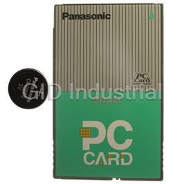
PANASONIC COMPUTER COMPONENTS BN-08MHSR

Description
PC CARD SRAM 8MB 68 PIN W/BATT
Part Number
BN-08MHSR
Price
Request Quote
Manufacturer
PANASONIC COMPUTER COMPONENTS
Lead Time
Request Quote
Category
PRODUCTS - B
Datasheet

Extracted Text
Panasonic PC Card BN-HSR Series Product Specification Rev3.0 Aug. 17 2001 JEIDA Ver.4.2/PCMCIA Rel.2.1 SRAM Card PRODUCT SPECIFICATION Model # : BN-064HSR(C) BN-128HSR(C) BN-256HSR(C) BN-512HSR(C) BN-01MHSR(C) BN-02MHSR(C) BN-04MHSR(C) BN-08MHSR(C) Published Aug. 17 2001 Drawn Checked Approved K.Toyokuni Y.Wada H.Hasegawa Contents Panasonic PC Card BN-HSR Series Product Specification Rev3.0 Aug. 17 2001 1. Scope ........................................................................................................................................................................1 2. Products Model # .....................................................................................................................................................1 3. Outline.......................................................................................................................................................................1 3.1. Physical Specification............................................................................................................................................................... 1 3.2. Temperature Condition............................................................................................................................................................. 1 4. Pin Assignment ........................................................................................................................................................2 5. Pin Definition............................................................................................................................................................2 6. Bias Power Supply Condition.................................................................................................................................3 6.1. Absolute Maximum Rating........................................................................................................................................................ 3 6.2. Recommended Operation Condition........................................................................................................................................ 3 7. Truth Table ...............................................................................................................................................................3 7.1. Common Memory Read Operation........................................................................................................................................... 3 7.2. Common Memory Write Operation........................................................................................................................................... 3 8. DC Characteristics...................................................................................................................................................4 8.1. General Characteristics............................................................................................................................................................ 4 8.2. Capacitance ............................................................................................................................................................................. 4 9. AC Characteristics ...................................................................................................................................................5 9.1. Read Cycle Timing (for Common memory and Attribute memory)........................................................................................... 5 9.2. Common memory Write Cycle Timing...................................................................................................................................... 7 9.3. Attribute Memory Write Timing................................................................................................................................................. 9 10. Power-up and down Sequence...........................................................................................................................11 10.1. Power-up and down Timing.................................................................................................................................................. 11 10.2. Status Output Timing............................................................................................................................................................ 12 11. Electrical Interface ...............................................................................................................................................13 12. Card Information Structure .................................................................................................................................14 13. Block Diagram......................................................................................................................................................15 14. Battery...................................................................................................................................................................17 14.1. Data Retention ..................................................................................................................................................................... 17 14.2. Battery Voltage Detection..................................................................................................................................................... 17 14.3. Battery Replacement............................................................................................................................................................ 17 Panasonic PC Card BN-HSR Series Product Specification Rev3.0 Aug. 17 2001 1. Scope This products specification relates to the Panasonic SRAM Card BN-HSR series. This SRAM Card conforms to updated Release 2.1 of PC Card standard specification which has been studied by Personal Computer Memory Card International Association (PCMCIA). 2. Products Model # Table 1 Products Model # Model # Common Memory Attribute Memory Battery Size (byte) Configuration Size(byte) Main Battery Sub Battery Configuration (Word×bit) BN-064HSR 64K FF Output No CR2025 Rechargable 64K×8 / 32K×16 BN-128HSR 128K Memory Lithum Battery Battery 128K×8 / 64K×16 BN-256HSR 256K 256K×8 / 128K×16 BN-512HSR 512K×8 / 256K×16 512K BN-01MHSR 1M×8 / 512K×16 1M BN-02MHSR 2M 2M×8 / 1M×16 BN-04MHSR 4M 4M×8 / 2M×16 BN-08MHSR 8M 8M×8 / 4M×16 BN-064HSRC 64K×8 / 32K×16 64K 2K×8 2K BN-128HSRC 128K×8 / 64K×16 128K BN-256HSRC 256K 256K×8 / 128K×16 BN-512HSRC 512K 512K×8 / 256K×16 BN-01MHSRC 1M 1M×8 / 512K×16 BN-02MHSRC 2M×8 / 1M×16 2M BN-04MHSRC 4M×8 / 2M×16 4M BN-08MHSRC 8M 8M×8 / 4M×16 3. Outline 3.1. Physical Specification Table 2 Physical Specification Length 85.6±0.2 mm Width 54.0±0.1 mm Thickness 3.3±0.1 mm Pin counts 68 pins 3.2. Temperature Condition Table 3 Temperature Condition Parameters Symbol Minimum Maximum Unit Operation Temperature T 0 60 OPT ℃ Storage Temperature T -20 70 ℃ STG 1 Panasonic PC Card BN-HSR Series Product Specification Rev3.0 Aug. 17 2001 4. Pin Assignment Pin # Signal Pin # Signal Pin # Signal Pin # Signal 1 GND 18 VPP1 35 GND 52 VPP2 2 D3 19 A16 36 CD1# 53 A22 3 D4 20 A15 37 D11 54 A23 4 D5 21 A12 38 D12 55 A24 5 D6 22 A7 39 D13 56 A25 6 D7 23 A6 40 D14 57 VS2# 7 CE1# 24 A5 41 D15 58 RESET 8 A10 25 A4 42 CE2# 59 WAIT# 9 OE# 26 A3 43 VS1# 60 RFU 10 A11 27 A2 44 RFU 61 REG# 11 A9 28 A1 45 RFU 62 BVD2 12 A8 29 A0 46 A17 63 BVD1 13 A13 30 D0 47 A18 64 D8 14 A14 31 D1 48 A19 65 D9 15 WE# 32 D2 49 A20 66 D10 16 READY 33 WP 50 A21 67 CD2# 17 VCC 34 GND 51 VCC 68 GND 5. Pin Definition � A0 - A25 Address input pins; Up to 64Kbyte memory space is supported. A25 is the most significantbit and A0 is the least significant bit. Address input pins exceeding its memory size are not connected in the card and are full-decoded in each memory space. � D0 - D15 Data I/O pins; D15 is the most significant bit and D0 is the least significant bit. � CE1#,CE2# Card Enable input pins; -CE1 controls even byte and -CE2 does odd byte. Both of them can be accessed on D0 - D7 by combination of A0, CE1# and CE2#. � WE# Write Enable input pin; This signal controls the write operation to the card. � OE# Output Enable input pin; This signal controls the read operation from the card. � REG# Attribute Memory Select input pin; When the low level assertion of this signal, the attribute memory space is enable. � READY Ready/ Busy output pin; This signal is NC (Not Connected with any card circuitry). � WP Write Protect output pin; WP is at high level during write protection and low level during write enable. This signal reflects write protection status in both common and attribute memory. � CD1#,CD2# Card Detection signal output pins; These output GND level and detect insertion or removal of the card. When they are pulled up to VCC at the system side, the insertion or removal of the card can be detected as digital signals through the buffer. � VS1#,VS2# Voltage Sense output pins; These signals are prepared to check whether the supported power supply voltage is 3.3 V or 5.0 V. In this card, both are NC indicates 5.0 V only supported. In order to apply this status at the system, the host must have pulled-up registor from 10 KΩ to � 100 KΩ on socket. � BVD1,BVD2 Battery Voltage Detection output pins � RESET Reset input pin; This signal is NC in this card. � WAIT# Wait output pin; This signal is NC in this card. � RFU Reserved for Future Use pins; This signal is NC in this card. � VCC Power supply pin; In this card, This signal is for +5V. � VPP1,VPP2 Peripheral power supply pins; these signals are NC in this card. � GND Ground pins 0V 2 Panasonic PC Card BN-HSR Series Product Specification Rev3.0 Aug. 17 2001 6. Bias Power Supply Condition 6.1. Absolute Maximum Rating Table 5 Absolute Maximum Rating Parameters Symbol Minimum Maximum Unit Power Supply Voltage V 0 6 V CC Input Voltage V -0.5 V+0.5 V I CC 6.2. Recommended Operation Condition Table 6 Recommended Operation Condition Parameters Symbol Minimum Typical Maximum Unit Power Supply Voltage V 4.5 5.0 5.5 V CC High Level Input Voltage V 2.2 V V IH CC Low Level Input Voltage V 0 0.8 V IL 7. Truth Table 7.1. Common Memory Read Operation Table 7 Common Memory Read Operation Function Mode REG# CE2# CE1# A0 OE# WE# D[15:8] D[7:0] Standby Mode X H H X X X Hi-z Hi-z Byte Access (8 bit) H H L L L H Hi-z Even Byte H H L H L H Hi-z Odd Byte Word Access (16 bit) H L L X L H Odd Byte Even Byte Odd-Byte-Only Access H L H X L H Odd Byte Hi-z Note X: can be either High level input or Low level input H: stands for High level input, L: stands for Low level input Hi-z: stands for High impedance 7.2. Common Memory Write Operation Table 8 Common Memory Write Operation Function Mode REG# CE2# CE1# A0 OE# WE# D[15:8] D[7:0] Standby Mode X H H X X X Hi-z Hi-z Byte Access (8 bit) H H L L H L Not Valid Even Byte H H L H H L Not Valid Odd Byte Word Access (16 bit) H L L X H L Odd Byte Even Byte Odd-Byte-Only Access H L H X H L Odd Byte Not Valid 3 Panasonic PC Card BN-HSR Series Product Specification Rev3.0 Aug. 17 2001 8. DC Characteristics 8.1. General Characteristics Table 11 General Characteristics V =5.0V±10%, Ta=0℃~60℃ CC Parameter Symbol Test Condition Value Unit Min. Typ. Max. Active Current I V =V Max.,CE1# or 80 mA CC1 CC CC CE#2=V IL t =200ns, I =0mA CR OUT I V =V Max.,CE1#=CE#2=V 150 mA CC2 CC CC IL t =200ns, I =0mA CR OUT Standby Current I V =V Max.,CE1#=CE#2=V 5 mA SB CC CC IH Empty charged to Sub Battery V =V Max.,CE1#=CE#2=V 100 150 μA CC CC IH Full charged to Sub Battery Input Leakage Current I V =V Max., V =V or GND LI CC CC IN CC ±10 μA Output Leakage Current I V =V Max., V =V or ±10 μA LO CC CC OUT CC GND Input Low Voltage V 0 0.8 V IL Input High Voltage V 2.2 V V IH CC Output Low Voltage V I=2.0mA 0.4 V OL OL Output High Voltage V I=-1.0mA 3.8 V OH OH 8.2. Capacitance Table 12 Capacitance (Ta=25℃, f=1.0MHz, not 100% tested) Symbol Maximum Value Unit Address signals /Control Signals C 100 pF IN Data signals C 50 pF I/O 4 Panasonic PC Card BN-HSR Series Product Specification Rev3.0 Aug. 17 2001 9. AC Characteristics 9.1. Read Cycle Timing (for Common memory and Attribute memory) Table 14 Read Cycle Timing (for Common memory and Attribute memory) V =5V±10%, Ta=0℃~60℃ CC Parameter Symbol Common Memory Attribute Memory Unit Min. Max. Min. Max. Read Cycle Time t 200 300 ns CR Address Access Time ta(A) 200 300 ns CE# Access Time ta(CE) 200 300 ns OE# Access Time ta(OE) 100 150 ns Output Disable Time from CE# Change tdis(CE) 90 100 ns Output Disable Time from OE# Change tdis(OE) 90 100 ns Output Enable Time from CE# Change ten(CE) 5 5 ns Output Enable Time from OE# Change ten(OE) 5 5 ns Data Valid Time from Address Change tv(A) 0 0 ns tcR ADDRESS REG# ta(A) tv(A) ta(CE) CE1#,CE2# tdis(CE) ta(OE) OE# tdis(OE) WE# DATA OUTPUT DATA Note) 1. Shaded sections denote areas where the level can be either high or low. 2. Output load : 1TTL + 100pF Figure 1 Common Memory Read Cycle Timing Chart 5 Panasonic PC Card BN-HSR Series Product Specification Rev3.0 Aug. 17 2001 tcR ADDRESS REG# ta(A) tv(A) ta(CE) CE1# tdis(CE) ta(OE) OE# tdis(OE) WE# DATA OUTPUT DATA Note) 1. Shaded sections denote areas where the level can be either high or low. 2. Output load : 1TTL + 100pF Figure 2 Attribute Memory Read Cycle timing Chart 6 Panasonic PC Card BN-HSR Series Product Specification Rev3.0 Aug. 17 2001 9.2. Common memory Write Cycle Timing Table 15 Common memory Write Cycle Timing V =5V±10%, Ta=0℃~60℃ CC Parameter Symbol Min. Typ. Max. Unit Write Cycle Time t 200 ns CW Write Pulse Width tw(WE) 120 ns Address Set-up Time tsu(A) 20 ns Address Set-up Time from WE# Change tsu(A-WEH) 140 ns CE# Set-up Time from WE# Change tsu(CE-WEH) 140 ns Data Set-up Time from WE# Change tsu(D) 60 ns Data Hold Time th(D) 30 ns Write Recovery Time trec(WE) 30 ns Output Disable Time from OE# tdis(OE) 90 ns Output Disable Time from CE# tdis(CE) 90 ns Output Enable Time from WE# ten(WE) 5 ns Output Enable Time from OE# ten(OE) 5 ns OE# Set-up Time from WE# tsu(OE-WE) 10 ns OE# Hold Time from WE# th(OE-WE) 10 ns tcW Address REG# tsu(A) tsu(CE-WEH) trec(WE) CE1# CE2# WE# tsu(D-WEH) th(D) D IN Input Data Note:*1 Shaded sections denote areas where the input level can be either High or Low. *2 When the data I/O signal is in output mode, input signal should not be applied to the card. Figure 3 CE# Contoroled Common Memory Write Cycle timing Chart 7 Panasonic PC Card BN-HSR Series Product Specification Rev3.0 Aug. 17 2001 tcW Address tsu(A-WEH) REG# tsu(CE-WEH) CE1# CE2# tsu(OE-WE) th(OE-WE) OE# trec(WE) tsu(A) tw(WE) WE# tsu(D-WEH) th(D) D IN Input Data ten(WE) tdis(WE) D OUT ten(OE) tdis(OE) Note: *1 Shaded sections denote areas where the input level can be either High or Low. *2 When the data I/O signal is in output mode, input signal should not be applied to the card. Figure 4 WE# Controlled Common Memory Write Cycle timing Chart 8 Panasonic PC Card BN-HSR Series Product Specification Rev3.0 Aug. 17 2001 9.3. Attribute Memory Write Timing Table 16 Attribute Memory Write Timing V =5V±10%, Ta=0℃-60℃ CC Parameter Symbol Min. Typ. Max. Unit Write Cycle Time tWC 1.0 ms Address Set-up Time tAS 10 ns Address Hold Time tAH 100 ns CE# Set-up Time tCS 20 ns CE# Hold Time tCH 20 ns CE# Write Pulse Width tCW 100 ns OE# Set-up Time tOES 15 ns OE# Hold Time tOEH 30 ns WE# Write Pulse Width tWP 100 ns WE# Write High Pulse Width tWEH 0.9 ms CE# Write High Pulse Width tCEH 0.9 ms Data Set-up Time tDS 100 ns Data Hold Time tDH 20 ns tWC Address tAS tAH REG# tCS tCH CE1# tOEH tOES OE# tWP tWEH WE# tDS tDH D IN Input Data Note: *1 Shaded sections denote area where the input level can be either High or Low. *2 When the data I/O signal is in output mode, input signal should not be applied to the card. Figure 5 WE# Controlled Attribute Memory Write Cycle timing Chart 9 Panasonic PC Card BN-HSR Series Product Specification Rev3.0 Aug. 17 2001 tWC Address tAS tAH REG# tCS tCH WE# tOEH tOES OE# tCW tCEH CE1# tDS tDH D IN Input Data Note:*1 Shaded sections denote area where the input level can be either High or Low. *2 When the data I/O signal is in output mode, input signal should not be applied to the card. Figure 6 CE# Controlled Attribute Memory Write Cycle timing Chart 10 Panasonic PC Card BN-HSR Series Product Specification Rev3.0 Aug. 17 2001 10. Power-up and down Sequence 10.1. Power-up and down Timing Table 17 Power-up and down Timing V =5.0V±10%, Ta=0℃~60℃ CC Parameter Symbol Test Condition Value Unit Min. Max. CE# Set-up Time from V tsu(V-CEL) 20 ms CC CC CE# Recovery Time from V trec(CEH-V ) 1.0 CC CC μs VCC Rising Time tpr from 0.1V to 0.9(V +5%) 0.1 300 ms CC CC VCC Falling Time tpf from 0.9(V -5%) to 0.1V 3.0 300 ms CC CC tpr V CC tsu(VCC) CE1#, CE2# tpf V CC trec(VCC) CE1#, CE2# Figure 7 Power-up and down Timing 11 Panasonic PC Card BN-HSR Series Product Specification Rev3.0 Aug. 17 2001 10.2. Status Output Timing Table 18 Status Output Timing V =5.0V±10%, Ta=0℃~60℃ CC Parameter Symbol Test Condition Value Unit Typ. Max. BVD Output Delay Time t 6 13 ms BVD WP Output Delay Time t 6 13 ms WPO 4.5V V CC t WPO WP t BVD BVD1 BVD2 Figure 8 Status Output Timing 12 Panasonic PC Card BN-HSR Series Product Specification Rev3.0 Aug. 17 2001 11. Electrical Interface Table 19 Electrical Interface Signal Type Memory Signal Electrical Interface Size Control Signals CE1# Pulled-up 20KΩ to V CC CE2# Pulled-up 20KΩ to V CC REG# Pulled-up 20KΩ to V CC OE# Pulled-up 20KΩ to V CC WE# Pulled-up 20KΩ to V CC RESET NC*1 Address Signals 64KB A[0:15] No Resistor*2 A[16:25] NC 128KB A[0:16] No Resistor A[17:25] NC 256KB A[0:17] No Resistor A[18:25] NC 512KB A[0:17] No Resistor A[18] Pulled-down 100KΩ to GND A[19:25] NC 1MB A[0:19] No Resistor A[20:25] NC 2MB A[0:20] No Resistor A[21:25] NC 4MB A[0:20] No Resistor A[21] Pulled-down 100KΩ to GND A[22:25] NC 8MB A[0:20] No Resistor A[21:22] Pulled-down 100KΩ to GND A[23:25] NC Data Signals D[0:15] No Resistor Output Signals BVD1 No Resistor BVD2 No Resistor READY NC WP No Resistor WAIT# NC CD1# GND Level CD2# GND Level Peripheral Power Supply V NC PP1 V NC PP2 Note *1 NC stands for Not Connected with any circuitry in the card. *2 “No Resistor” means signal is directly connected with circuitry in the card 13 Panasonic PC Card BN-HSR Series Product Specification Rev3.0 Aug. 17 2001 12. Card Information Structure BN-HSRC type in this series includes some Card Information structure (CIS) at the shipment which shares just 6 byte on 2 Kbyte attribute memory plane. This content is as follows. It’s possible for user to store favorite CIS by additional writing because of EEPROM device as attribute memory. Please refer to electrical specification considering attribute memory. Address Data Symbol Description 00h 01h CISTPL_DEVICE_C Common Memory Device Information Tuple 02h 03h TPL_LINK 04h 62h DTYPE_SRAM, DSPEED_200NS SRAM, 200ns, WP flag Available 06h 0Bh 64KB 1Bh 128KB 3Bh 256KB 7Bh 512KB FBh 1MB 1Dh 2MB 3Dh 4MB 7Dh 8MB 08h FFh End of Common Memory Device Info Tuple 0Ah FFh CISTPL_END End of Tuple List 14 Panasonic PC Card BN-HSR Series Product Specification Rev3.0 Aug. 17 2001 13. Block Diagram Data Bus Control Signal 5V MEMORY CONTROL SRAM IC LSI SW WP JEIDA/ Address Bus PCMCIA EEPROM Interface IC *1 Vout *1 In BN-HSR type, EEPROM is not equipped. Vcc POWER BVD CONTROL IC CR2025 Vcc C Sub Battery CD1#,CD2 GND Figure 9 BN-064~01MHSR(C) type Block Diagram Data Bus 3 to 5V 3 to 5V conversion MEMORY conversion Control Signal ciurcuitry CONTROL ciurcuitry 3V 3V LSI SRAM IC SW WP JEIDA/ Address Bus PCMCIA EEPROM Interface IC *1 Vcc Regulator *1 In BN-HSR type, EEPROM is not equipped. BVD POWER CR2025 CONTROL IC Sub Battery Vcc C CD1#,CD2 GND Figure 10 BN-02M~08MHSR(C) type Block Diagram 15 Panasonic PC Card BN-HSR Series Product Specification Rev3.0 Aug. 17 2001 16 Panasonic PC Card BN-HSR Series Product Specification Rev3.0 Aug. 17 2001 14. Battery 14.1. Data Retention Table 21 Data Retention Memory Size Memory Back-up time Ta=25℃ 64Kbyte 5 years 128Kbyte 5 years 256Kbyte 5 years 512Kbyte 5 years 1Mbyte 5 years 2Mbyte 3 years 4Mbyte 1 years 8Mbyte 0.5 years Note:*1 CR2025 battery produced by Panasonic should be used for main back-up battery of this card. *2 These values are estimated back-up time when Panasonic CR2025 is used for back-up. 14.2. Battery Voltage Detection Table 22 Battery Voltage Detection BVD1(#63) BVD2(#62) Definition H H Battery Operational H L Battery Operational, but battery should be replaced. L H Not available data retention, battery should be replaced. L L Not available data retention, battery should be replaced. Note: “H” and “L” in the table indicate High and Low Output Level each other. 14.3. Battery Replacement This card also includes Sub Battery which becomes back-up battery during replacement of main battery CR2025. It’s possible to replace new CR2025 within approximately 1 hour without external power supply 17 Panasonic PC Card BN-HSR Series Product Specification Rev3.0 Aug. 17 2001 Revision History Rev. Chapter # Title Revision Contents Date # Previous Updated 1 6/9/95 Nezu 1.01 8. DC Characteristic Stand-by Current 7/21/95 Nezu 8.1 2mA(typ.) , 100μA(typ.) , 3mA(Max.) 150μA(Max.) when sub-battery is when sub-battery is full-charged full-charged 9. AC Characteristic Drawn new 10. Power-up & down 12. Block Diagram 1.1 Add BN-HSRC type 9/8/95 Nezu Add 4Mbyte SRAM 11. Electrical 512K to 2Mbyte 512K to 2Mbyte Interface A18 is pulled-down by A18 is directly connec-ted with memory chip 100KΩ resistor. without pulled-down resistor. 12. CIS Add CIS table 14.1 Data Retention 5 years for 1MB 4 years for 1MB 3 years for 2MB 2 years for 2MB 1.2 Add 64K and 128K 11/17/95 Nezu byte SRAM 10.2 Status Output t=10ms(Typ.) t =10μs(Typ.) BVD BVD Timing 2.0 10.2 Status Output t =10ms(Typ.) t =6ms(Typ.) 10/31/96 Toyokuni BVD BVD Timing t =1.5ms(Typ.) =13ms(Max.) WPD =2.0mS(Max.) t =6ms(Typ.) WPD =13mS(Max.) 2.0 11 Electrical Interface 10/31/96 Toyokuni for Address Signal 128Kbyte Pulled-down 100KΩ to GND A16 : No Resistor 512Kbyte No Resistor Pulled-down 100KΩ to GND A18 : 1Mbyte Pulled-down 100KΩ to GND No Resistor A19 : 2Mbyte Pulled-down 100KΩ to GND No Resistor A19 : 4Mbyte Pulled-down 100KΩ to GND No Resistor A19 : 2.1 13.1 Data Retention 5/29/97 Toyokuni 1Mbyte : 4years 5years 2Mbyte : 2years 3years 2.2 2,11,13 7/9/97 Toyokuni Add Model# BN-08MHSR(C) 18 Panasonic PC Card BN-HSR Series Product Specification Rev3.0 Aug. 17 2001 Revision History Rev. Chapter Title Revision Contents Date # # Previous Updated 3.0 11 Electrical Interface 9/17/01 Toyokuni for Address Signal 2Mbyte Pulled-down 100KΩ to GND A20 : No Resistor 4Mbyte Pulled-down 100KΩ to GND No Resistor A20 : 4Mbyte Pulled-down 100KΩ to GND No Resistor A19,A20 : 13 Block Diagram Configured by Configured by 5V-SRAM IC (BN-02MHSR(C) 3V-SRAM IC ~BN-08MHSRC) w/ 3 to 5V conversion ciurcuitry 19
Frequently asked questions
What makes Elite.Parts unique?

What kind of warranty will the BN-08MHSR have?
Which carriers does Elite.Parts work with?
Will Elite.Parts sell to me even though I live outside the USA?
I have a preferred payment method. Will Elite.Parts accept it?


What they say about us
FANTASTIC RESOURCE
One of our top priorities is maintaining our business with precision, and we are constantly looking for affiliates that can help us achieve our goal. With the aid of GID Industrial, our obsolete product management has never been more efficient. They have been a great resource to our company, and have quickly become a go-to supplier on our list!
Bucher Emhart Glass
EXCELLENT SERVICE
With our strict fundamentals and high expectations, we were surprised when we came across GID Industrial and their competitive pricing. When we approached them with our issue, they were incredibly confident in being able to provide us with a seamless solution at the best price for us. GID Industrial quickly understood our needs and provided us with excellent service, as well as fully tested product to ensure what we received would be the right fit for our company.
Fuji
HARD TO FIND A BETTER PROVIDER
Our company provides services to aid in the manufacture of technological products, such as semiconductors and flat panel displays, and often searching for distributors of obsolete product we require can waste time and money. Finding GID Industrial proved to be a great asset to our company, with cost effective solutions and superior knowledge on all of their materials, it’d be hard to find a better provider of obsolete or hard to find products.
Applied Materials
CONSISTENTLY DELIVERS QUALITY SOLUTIONS
Over the years, the equipment used in our company becomes discontinued, but they’re still of great use to us and our customers. Once these products are no longer available through the manufacturer, finding a reliable, quick supplier is a necessity, and luckily for us, GID Industrial has provided the most trustworthy, quality solutions to our obsolete component needs.
Nidec Vamco
TERRIFIC RESOURCE
This company has been a terrific help to us (I work for Trican Well Service) in sourcing the Micron Ram Memory we needed for our Siemens computers. Great service! And great pricing! I know when the product is shipping and when it will arrive, all the way through the ordering process.
Trican Well Service
GO TO SOURCE
When I can't find an obsolete part, I first call GID and they'll come up with my parts every time. Great customer service and follow up as well. Scott emails me from time to time to touch base and see if we're having trouble finding something.....which is often with our 25 yr old equipment.
ConAgra Foods