

 Manufacturers
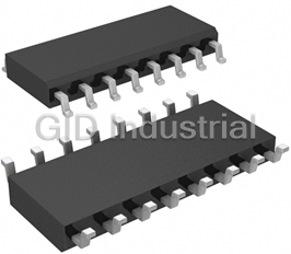
ON SEMICONDUCTOR SN74LS374DW
Description
ON Semiconductor SN74LS374DW Latch - TTL; 5.0 V (Typ.); -2.60 mA (Max.); 2.0 V (Min.); 0.80 V (Max.); 0 degC
Part Number
SN74LS374DW
Price
Request Quote
Manufacturer
ON SEMICONDUCTOR
Lead Time
Request Quote
Category
PRODUCTS - S
Specifications
Input High Current
0.1 mA
Input Low Current
–0.4 mA
Output Off Current High
20 mA
Output Off Current Low
–20 mA
Power Supply Current
40 mA
Short Circuit Current
–30 Min, –130 Max mA
Features
- 3-State Outputs for Bus Interfacing
- Buffered Positive Edge-Triggered Clock
- Edge-Triggered D-Type Inputs
- Eight Latches in a Single Package
- Hysteresis on Clock Input to Improve Noise Margin
- Hysteresis on Latch Enable
- Input Clamp Diodes Limit High Speed Termination Effects
Datasheet

Extracted Text
SN74LS373, SN74LS374 Octal Transparent Latch with 3-State Outputs; Octal D-Type Flip-Flop with 3-State Output http://onsemi.com The SN74LS373 consists of eight latches with 3-state outputs for bus organized system applications. The flip-flops appear transparent LOW to the data (data changes asynchronously) when Latch Enable (LE) is HIGH. When LE is LOW, the data that meets the setup times is POWER latched. Data appears on the bus when the Output Enable (OE) is SCHOTTKY LOW. When OE is HIGH the bus output is in the high impedance state. The SN74LS374 is a high-speed, low-power Octal D-type Flip-Flop MARKING featuring separate D-type inputs for each flip-flop and 3-state outputs DIAGRAMS for bus oriented applications. A buffered Clock (CP) and Output Enable (OE) is common to all flip-flops. The SN74LS374 is manufactured using advanced Low Power Schottky technology and is SN74LS37xN compatible with all ON Semiconductor TTL families. AWLYYWW • Eight Latches in a Single Package 1 20 • 3-State Outputs for Bus Interfacing 1 PDIP–20 • Hysteresis on Latch Enable N SUFFIX • Edge-Triggered D-Type Inputs CASE 738 • Buffered Positive Edge-Triggered Clock • Hysteresis on Clock Input to Improve Noise Margin • Input Clamp Diodes Limit High Speed Termination Effects LS37x AWLYYWW 20 GUARANTEED OPERATING RANGES 1 1 Symbol Parameter Min Typ Max Unit SOIC–20 V Supply Voltage 4.75 5.0 5.25 V CC DW SUFFIX T Operating Ambient 0 25 70 °C CASE 751D A Temperature Range I Output Current – High –2.6 mA OH I Output Current – Low 24 mA OL 74LS37x AWLYWW 20 1 SOEIAJ–20 1 M SUFFIX CASE 967 x = 3 or 4 A = Assembly Location WL = Wafer Lot YY = Year WW = Work Week ORDERING INFORMATION See detailed ordering and shipping information in the package dimensions section on page 6 of this data sheet. Semiconductor Components Industries, LLC, 2001 1 Publication Order Number: October, 2001 – Rev. 8 SN74LS373/D SN74LS373, SN74LS374 CONNECTION DIAGRAM DIP (TOP VIEW) SN74LS374 SN74LS373 O LE V O D D O O D D 4 V O D D O O D D O CP CC 7 7 6 6 5 5 4 CC 7 7 6 6 5 5 4 4 20 19 18 17 16 15 14 13 12 11 20 19 18 17 16 15 14 13 12 11 12 3 4 5 6 8 910 7 12 3 4 5 6 7 8 910 NOTE: OE O D D O O D D O GND 0 0 1 1 2 2 3 3 OE O D D O O D D O GND 0 0 1 1 2 2 3 3 The Flatpak version has the same pinouts (Connection Diagram) as the Dual In�Line Package. LOADING (Note a) HIGH LOW PIN NAMES D - D Data Inputs 0.5 U.L. 0.25 U.L. 0 7 LE Latch Enable (Active HIGH) Input 0.5 U.L. 0.25 U.L. CP Clock (Active HIGH Going Edge) Input 0.5 U.L. 0.25 U.L. OE Output Enable (Active LOW) Input 0.5 U.L. 0.25 U.L. O - O Outputs 65 U.L. 15 U.L. 0 7 NOTES: �a) 1 TTL Unit Load (U.L.) = 40 �A HIGH/1.6 mA LOW. TRUTH TABLE LS373 LS374 D LE OE O D LE OE O n n n n H H L H H L H L H L L L L L X L L Q X X H Z* 0 X X H Z* H = HIGH Voltage Level L = LOW Voltage Level X = Immaterial Z = High Impedance * Note: Contents of flip-flops unaffected by the state of the Output Enable input (OE). http://onsemi.com 2 SN74LS373, SN74LS374 LOGIC DIAGRAMS SN74LS373 3 4 7 8 13 14 17 18 V = PIN 20 CC GND = PIN 10 D D D D D D D D 0 1 2 3 4 5 6 7 = PIN NUMBERS D D D D D D D D LATCH Q Q Q Q Q Q Q Q ENABLE G G G G G G G G LE 11 OE 1 O O O O O O O O 0 1 2 3 4 5 6 7 26 5 9 12 15 16 19 SN74LS374 3 4 7 8 13 14 17 18 D D D D D D D D 11 0 1 2 3 4 5 6 7 CP CP D CP D CP D CP D CP D CP D CP D CP D QQ QQ QQ QQ QQ QQ QQ QQ OE 1 O O O O O O O O 0 1 2 3 4 5 6 7 26 5 9 12 15 16 19 DC CHARACTERISTICS OVER OPERATING TEMPERATURE RANGE (unless otherwise specified) Limits Min Typ Max Symbol Parameter Unit Test Conditions Guaranteed Input HIGH Voltage for V Input HIGH Voltage 2.0 V IH All Inputs 0.8 Guaranteed Input LOW Voltage for V Input LOW Voltage V IL All Inputs V Input Clamp Diode Voltage –0.65 –1.5 V V = MIN, I = –18 mA IK CC IN V = MIN, I = MAX, V = V CC OH IN IH V Output HIGH Voltage 2.4 3.1 V OH or V per Truth Table IL V = V MIN, 0.25 0.4 V I = 12 mA CC CC OL V V Out Output LOW V put LOW Voltage oltage V V = V V or V or V OL OL IN IN IL IL IH IH 0.35 0.5 V I = 24 mA OL per Truth Table I Output Off Current HIGH 20 μA V = MAX, V = 2.7 V OZH CC OUT I Output Off Current LOW –20 μA V = MAX, V = 0.4 V OZL CC OUT 20 μA V = MAX, V = 2.7 V CC IN II In Input HIGH Current put HIGH Current IH IH 0.1 mA V = MAX, V = 7.0 V CC IN I Input LOW Current –0.4 mA V = MAX, V = 0.4 V IL CC IN I Short Circuit Current (Note 1) –30 –130 mA V = MAX OS CC I Power Supply Current 40 mA V = MAX CC CC 1. Not more than one output should be shorted at a time, nor for more than 1 second. http://onsemi.com 3 SN74LS373, SN74LS374 AC CHARACTERISTICS (T = 25°C, V = 5.0 V) A CC Limits LS373 LS374 Symbol Parameter Min Typ Max Min Typ Max Unit Test Conditions f Maximum Clock Frequency 35 50 MHz MAX t Propagation Delay, 12 18 PLH ns t Data to Output 12 18 PHL C =45 pF C = 45 pF, L L t Clock or Enable 20 30 15 28 PLH R = 667 Ω L ns t to Output 18 30 19 28 PHL t 15 28 20 28 PZH Output Enable Time ns t 25 36 21 28 PZL t 12 20 12 20 PHZ Output Disable Time ns C = 5.0 pF L t 15 25 15 25 PLZ AC SETUP REQUIREMENTS (T = 25°C, V = 5.0 V) A CC Limits LS373 LS374 Min Max Min Max Symbol Parameter Unit t Clock Pulse Width 15 15 ns W t Setup Time 5.0 20 ns s t Hold Time 20 0 ns h DEFINITION OF TERMS SETUP TIME (t ) — is defined as the minimum time HOLD TIME (t ) — is defined as the minimum time s h required for the correct logic level to be present at the logic following the LE transition from HIGH-to-LOW that the input prior to LE transition from HIGH-to-LOW in order to logic level must be maintained at the input in order to ensure be recognized and transferred to the outputs. continued recognition. SN74LS373 AC WAVEFORMS t t W W 1.3 V LE t t s h D n t t PLH PHL OUTPUT Figure 1. OE OE 1.3 V 1.3 V 1.3 V 1.3 V t t t t PZL PLZ PZH PHZ V OH V OUT 1.3 V 1.3 V 1.3 V V 1.3 V OUT V OL 0.5 V 0.5 V Figure 2. Figure 3. http://onsemi.com 4 SN74LS373, SN74LS374 SN74LS373 AC LOAD CIRCUIT V CC SWITCH POSITIONS R L SYMBOL SW1 SW2 t Open Closed PZH SW1 t Closed Open PZL t Closed Closed PLZ TO OUTPUT UNDER TEST t Closed Closed PHZ 5.0 k Ω C * SW2 L * Includes Jig and Probe Capacitance. Figure 4. SN74LS374 AC WAVEFORMS t Ht L W W OE 1.3 V 1.3 V CP 1.3 V 1.3 V 1.3 V t t h t PZL t PLZ s V ≈ 1.3 V OUT 1.3 V D 1.3 V n V OL t t PLH PHL 0.5 V Figure 6. OUTPUT 1.3 V 1.3 V Figure 5. OE 1.3 V 1.3 V t t PZH PHZ ≥ V OH ≈ 1.3 V V 1.3 V OUT 0.5 V Figure 7. http://onsemi.com 5 SN74LS373, SN74LS374 SN74LS374 AC LOAD CIRCUIT V CC SWITCH POSITIONS SYMBOL SW1 SW2 R L t Open Closed PZH t Closed Open PZL SW1 t Closed Closed PLZ t Closed Closed TO OUTPUT PHZ UNDER TEST 5.0 k Ω C * SW2 L * Includes Jig and Probe Capacitance. Figure 8. DEVICE ORDERING INFORMATION Device Order Number Package Type Tape and Reel Size SN74LS373N PDIP–20 1440 Units/Box SN74LS373DW SOIC–WIDE 38 Units/Rail SN74LS373DWR2 SOIC–WIDE 2500/Tape and Reel SN74LS373M SOEIAJ–20 See Note 2 SN74LS373MEL SOEIAJ–20 See Note 2 SN74LS374N PDIP–20 1440 Units/Box SN74LS374DW SOIC–WIDE 38 Units/Rail SN74LS374DWR2 SOIC–WIDE 2500/Tape and Reel SN74LS374M SOEIAJ–20 See Note 2 SN74LS374MEL SOEIAJ–20 See Note 2 2. For ordering information on the EIAJ version of the SOIC package, please contact your local ON Semiconductor representative. http://onsemi.com 6 SN74LS373, SN74LS374 PACKAGE DIMENSIONS N SUFFIX PLASTIC PACKAGE CASE 738–03 ISSUE E –A– NOTES: 1. DIMENSIONING AND TOLERANCING PER ANSI Y14.5M, 1982. 20 11 2. CONTROLLING DIMENSION: INCH. B 3. DIMENSION L TO CENTER OF LEAD WHEN FORMED PARALLEL. 1 10 4. DIMENSION B DOES NOT INCLUDE MOLD FLASH. L C INCHES MILLIMETERS DIM MIN MAX MIN MAX A 1.010 1.070 25.66 27.17 B 0.240 0.260 6.10 6.60 C 0.150 0.180 3.81 4.57 –T– K D 0.015 0.022 0.39 0.55 SEATING E 0.050 BSC 1.27 BSC PLANE M F 0.050 0.070 1.27 1.77 E N G 0.100 BSC 2.54 BSC J 0.008 0.015 0.21 0.38 G F K 0.110 0.140 2.80 3.55 J 20 PL L 0.300 BSC 7.62 BSC D 20 PL M M 0.25 (0.010) T B M 0 15 0 15 �� �� M M N 0.020 0.040 0.51 1.01 0.25 (0.010) T A D SUFFIX PLASTIC SOIC PACKAGE CASE 751D–05 ISSUE F D A � NOTES: 1. DIMENSIONS ARE IN MILLIMETERS. 20 11 2. INTERPRET DIMENSIONS AND TOLERANCES PER ASME Y14.5M, 1994. 3. DIMENSIONS D AND E DO NOT INCLUDE MOLD PROTRUSION. E 4. MAXIMUM MOLD PROTRUSION 0.15 PER SIDE. 5. DIMENSION B DOES NOT INCLUDE DAMBAR PROTRUSION. ALLOWABLE PROTRUSION SHALL BE 0.13 TOTAL IN EXCESS OF B DIMENSION AT 1 10 MAXIMUM MATERIAL CONDITION. MILLIMETERS DIM MIN MAX B A 2.35 2.65 20X B A1 0.10 0.25 M T S S 0.25 A B B 0.35 0.49 C 0.23 0.32 D 12.65 12.95 E 7.40 7.60 e 1.27 BSC A H 10.05 10.55 h 0.25 0.75 L 0.50 0.90 SEATING � 0 7 PLANE �� 18X e A1 C T http://onsemi.com 7 10X H M M 0.25 B h X 45 � L SN74LS373, SN74LS374 PACKAGE DIMENSIONS M SUFFIX SOEIAJ PACKAGE CASE 967–01 ISSUE O NOTES: 1. DIMENSIONING AND TOLERANCING PER ANSI Y14.5M, 1982. 2. CONTROLLING DIMENSION: MILLIMETER. 3. DIMENSIONS D AND E DO NOT INCLUDE MOLD FLASH OR PROTRUSIONS AND ARE MEASURED L 20 11 E AT THE PARTING LINE. MOLD FLASH OR PROTRUSIONS SHALL NOT EXCEED 0.15 (0.006) Q 1 PER SIDE. 4. TERMINAL NUMBERS ARE SHOWN FOR E H � E M REFERENCE ONLY. 5. THE LEAD WIDTH DIMENSION (b) DOES NOT INCLUDE DAMBAR PROTRUSION. ALLOWABLE DAMBAR PROTRUSION SHALL BE 0.08 (0.003) L 110 TOTAL IN EXCESS OF THE LEAD WIDTH DIMENSION AT MAXIMUM MATERIAL CONDITION. DETAIL P DAMBAR CANNOT BE LOCATED ON THE LOWER Z RADIUS OR THE FOOT. MINIMUM SPACE BETWEEN PROTRUSIONS AND ADJACENT LEAD D TO BE 0.46 ( 0.018). VIEW P MILLIMETERS INCHES e A DIM MIN MAX MIN MAX c A --- 2.05 --- 0.081 A 0.05 0.20 0.002 0.008 1 b 0.35 0.50 0.014 0.020 c 0.18 0.27 0.007 0.011 D 12.35 12.80 0.486 0.504 A b 1 E 5.10 5.45 0.201 0.215 e 1.27 BSC 0.050 BSC M 0.13 (0.005) 0.10 (0.004) H 7.40 8.20 0.291 0.323 E L 0.50 0.85 0.020 0.033 L 1.10 1.50 0.043 0.059 E M 0 10 0 10 � � � � Q 0.70 0.90 0.028 0.035 1 Z --- 0.81 --- 0.032 ON Semiconductor and are trademarks of Semiconductor Components Industries, LLC (SCILLC). SCILLC reserves the right to make changes without further notice to any products herein. SCILLC makes no warranty, representation or guarantee regarding the suitability of its products for any particular purpose, nor does SCILLC assume any liability arising out of the application or use of any product or circuit, and specifically disclaims any and all liability, including without limitation special, consequential or incidental damages. “Typical” parameters which may be provided in SCILLC data sheets and/or specifications can and do vary in different applications and actual performance may vary over time. All operating parameters, including “Typicals” must be validated for each customer application by customer’s technical experts. SCILLC does not convey any license under its patent rights nor the rights of others. SCILLC products are not designed, intended, or authorized for use as components in systems intended for surgical implant into the body, or other applications intended to support or sustain life, or for any other application in which the failure of the SCILLC product could create a situation where personal injury or death may occur. Should Buyer purchase or use SCILLC products for any such unintended or unauthorized application, Buyer shall indemnify and hold SCILLC and its officers, employees, subsidiaries, affiliates, and distributors harmless against all claims, costs, damages, and expenses, and reasonable attorney fees arising out of, directly or indirectly, any claim of personal injury or death associated with such unintended or unauthorized use, even if such claim alleges that SCILLC was negligent regarding the design or manufacture of the part. SCILLC is an Equal Opportunity/Affirmative Action Employer. PUBLICATION ORDERING INFORMATION Literature Fulfillment: JAPAN: ON Semiconductor, Japan Customer Focus Center Literature Distribution Center for ON Semiconductor 4–32–1 Nishi–Gotanda, Shinagawa–ku, Tokyo, Japan 141–0031 P.O. Box 5163, Denver, Colorado 80217 USA Phone: 81–3–5740–2700 Phone: 303–675–2175 or 800–344–3860 Toll Free USA/Canada Email: r14525@onsemi.com Fax: 303–675–2176 or 800–344–3867 Toll Free USA/Canada ON Semiconductor Website: http://onsemi.com Email: ONlit@hibbertco.com For additional information, please contact your local N. American Technical Support: 800–282–9855 Toll Free USA/Canada Sales Representative. SN74LS373/D http://onsemi.com 8
Frequently asked questions
What makes Elite.Parts unique?

What kind of warranty will the SN74LS374DW have?
Which carriers does Elite.Parts work with?
Will Elite.Parts sell to me even though I live outside the USA?
I have a preferred payment method. Will Elite.Parts accept it?
Why buy from GID?

Quality
We are industry veterans who take pride in our work

Protection
Avoid the dangers of risky trading in the gray market

Access
Our network of suppliers is ready and at your disposal

Savings
Maintain legacy systems to prevent costly downtime

Speed
Time is of the essence, and we are respectful of yours
Related Products

LOG CMOS BIDIRCT 16BIT RoHS Compliant: No
LOG CMOS BIDIRCT 16BIT RoHS Compliant: Yes
ZEN MOSRB MINI 500W 100V
TVS Diode
500 Watt Peak Power MiniMOSORB Zener Transient Voltage Suppressors
ZEN MOSRB MINI 500W 10V
Request a Quote

The quote request has been received
Close

Facing challenges or have inquiries? Feel free to contact us!
Call Us +1-469-283-2440
What they say about us
FANTASTIC RESOURCE
One of our top priorities is maintaining our business with precision, and we are constantly looking for affiliates that can help us achieve our goal. With the aid of GID Industrial, our obsolete product management has never been more efficient. They have been a great resource to our company, and have quickly become a go-to supplier on our list!
Bucher Emhart Glass
EXCELLENT SERVICE
With our strict fundamentals and high expectations, we were surprised when we came across GID Industrial and their competitive pricing. When we approached them with our issue, they were incredibly confident in being able to provide us with a seamless solution at the best price for us. GID Industrial quickly understood our needs and provided us with excellent service, as well as fully tested product to ensure what we received would be the right fit for our company.
Fuji
HARD TO FIND A BETTER PROVIDER
Our company provides services to aid in the manufacture of technological products, such as semiconductors and flat panel displays, and often searching for distributors of obsolete product we require can waste time and money. Finding GID Industrial proved to be a great asset to our company, with cost effective solutions and superior knowledge on all of their materials, it’d be hard to find a better provider of obsolete or hard to find products.
Applied Materials
CONSISTENTLY DELIVERS QUALITY SOLUTIONS
Over the years, the equipment used in our company becomes discontinued, but they’re still of great use to us and our customers. Once these products are no longer available through the manufacturer, finding a reliable, quick supplier is a necessity, and luckily for us, GID Industrial has provided the most trustworthy, quality solutions to our obsolete component needs.
Nidec Vamco
TERRIFIC RESOURCE
This company has been a terrific help to us (I work for Trican Well Service) in sourcing the Micron Ram Memory we needed for our Siemens computers. Great service! And great pricing! I know when the product is shipping and when it will arrive, all the way through the ordering process.
Trican Well Service
GO TO SOURCE
When I can't find an obsolete part, I first call GID and they'll come up with my parts every time. Great customer service and follow up as well. Scott emails me from time to time to touch base and see if we're having trouble finding something.....which is often with our 25 yr old equipment.
ConAgra Foods