

 Manufacturers
ON SEMICONDUCTOR BCP68T1

Description
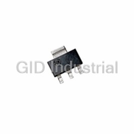
TRANS NPN AUDIO 1A 25V SOT223
Part Number
BCP68T1
Price
Request Quote
Manufacturer
ON SEMICONDUCTOR
Lead Time
Request Quote
Category
PRODUCTS - B
Datasheet

Extracted Text
ON Semiconductor� BCP68T1 NPN Silicon ON Semiconductor Preferred Device Epitaxial Transistor MEDIUM POWER This NPN Silicon Epitaxial Transistor is designed for use in low NPN SILICON voltage, high current applications. The device is housed in the HIGH CURRENT SOT-223 package, which is designed for medium power surface TRANSISTOR mount applications. SURFACE MOUNT • High Current: I = 1.0 Amp C • The SOT-223 Package can be soldered using wave or reflow. • SOT-223 package ensures level mounting, resulting in improved 4 thermal conduction, and allows visual inspection of soldered joints. The formed leads absorb thermal stress during soldering, eliminating 1 2 the possibility of damage to the die 3 • Available in 12 mm Tape and Reel CASE 318E-04, STYLE 1 Use BCP68T1 to order the 7 inch/1000 unit reel. TO-261AA Use BCP68T3 to order the 13 inch/4000 unit reel. • The PNP Complement is BCP69T1 COLLECTOR 2,4 BASE 1 EMITTER 3 MAXIMUM RATINGS (T = 25°C unless otherwise noted) C Rating Symbol Value Unit Collector-Emitter Voltage V 25 Vdc CEO Collector-Base Voltage V 20 Vdc CBO Emitter-Base Voltage V 5 Vdc EBO Collector Current I 1 Adc C (1) Total Power Dissipation @ T = 25°C P 1.5 Watts A D Derate above 25°C 12 mW/°C Operating and Storage Temperature Range T , T –65 to 150 °C J stg DEVICE MARKING CA THERMAL CHARACTERISTICS Characteristic Symbol Max Unit Thermal Resistance — Junction-to-Ambient (surface mounted) R 83.3 °C/W θJA Maximum Temperature for Soldering Purposes T 260 °C L Time in Solder Bath 10 Sec 1. Device mounted on a FR-4 glass epoxy printed circuit board 1.575 in. x 1.575 in. x 0.0625 in.; mounting pad for the collector lead = 0.93 sq. in. Preferred devices are ON Semiconductor recommended choices for future use and best overall value. Semiconductor Components Industries, LLC, 2001 1 Publication Order Number: November, 2001 – Rev. 3 BCP68T1/D BCP68T1 ELECTRICAL CHARACTERISTICS (T = 25°C unless otherwise noted) A Characteristics Symbol Min Typ Max Unit OFF CHARACTERISTICS Collector-Emitter Breakdown Voltage V 25 — — Vdc (BR)CES (I = 100 μAdc, I = 0) C E Collector-Emitter Breakdown Voltage V 20 — — Vdc (BR)CEO (I = 1.0 mAdc, I = 0) C B Emitter-Base Breakdown Voltage V 5.0 — — Vdc (BR)EBO (I = 10 μAdc, I = 0) E C Collector-Base Cutoff Current I — — 10 μAdc CBO (V = 25 Vdc, I = 0) CB E Emitter-Base Cutoff Current I — — 10 μAdc EBO (V = 5.0 Vdc, I = 0) EB C ON CHARACTERISTICS (2) DC Current Gain h — FE (I = 5.0 mAdc, V = 10 Vdc) 50 — — C CE (I = 500 mAdc, V = 1.0 Vdc) 85 — 375 C CE (I = 1.0 Adc, V = 1.0 Vdc) 60 — — C CE Collector-Emitter Saturation Voltage V — — 0.5 Vdc CE(sat) (I = 1.0 Adc, I = 100 mAdc) C B Base-Emitter On Voltage V — — 1.0 Vdc BE(on) (I = 1.0 Adc, V = 1.0 Vdc) C CE DYNAMIC CHARACTERISTICS Current-Gain — Bandwidth Product f — 60 — MHz T (I = 10 mAdc, V = 5.0 Vdc) C CE 2. Pulse Test: Pulse Width ≤ 300 μs, Duty Cycle ≤ 2.0% TYPICAL ELECTRICAL CHARACTERISTICS 300 200 300 T = 125 °C J 200 = 25 °C 100 100 = -55 °C 70 V = 10 V CE T = 25 °C J 50 f = 30 MHz V = 1.0 V CE 10 30 1.0 10 100 1000 10 100 200 1000 I , COLLECTOR CURRENT (mA) I , COLLECTOR CURRENT (mA) C C Figure 1. DC Current Gain Figure 2. Current-Gain-Bandwidth Product http://onsemi.com 2 h , DC CURRENT GAIN FE f�, CURRENT�GAIN�BANDWIDTH PRODUCT (MHz) T BCP68T1 TYPICAL ELECTRICAL CHARACTERISTICS 1.0 80 T = 25 °C J T = 25 °C J V @ I /I = 10 BE(sat) C B 0.8 70 0.6 60 V @ V = 1.0 V BE(on) CE 0.4 50 0.2 40 V @ I /I = 10 CE(sat) C B 30 0 1.0 10 100 1000 0 1.0 2.0 3.0 4.0 5.0 I , COLLECTOR CURRENT (mA) V , REVERSE VOLTAGE (VOLTS) C R Figure 3. “On” Voltage Figure 4. Capacitance 25 -�0.8 T = 25 °C J -1.2 20 -1.6 R for V θVB BE 15 -�2.0 10 -�2.4 -�2.8 5.0 0 5.0 10 15 20 1.0 10 100 1000 V , REVERSE VOLTAGE (VOLTS) I , COLLECTOR CURRENT (mA) R C Figure 5. Capacitance Figure 6. Base-Emitter Temperature Coefficient 1.0 T = 25 °C J 0.8 0.6 = 1000 mA I = 10 mA = 100 mA 0.4 = 50 mA C 0.2 = 500 mA 0 0.01 0.1 1.0 10 100 I , BASE CURRENT (mA) B Figure 7. Saturation Region http://onsemi.com 3 C , CAPACITANCE (pF) V, VOLTAGE (VOLTS) ob V , COLLECTOR VOLTAGE (V) CE R , TEMPERATURE COEFFICIENT (mV/ C) ° C , CAPACITANCE (pF) θVB ib θ BCP68T1 INFORMATION FOR USING THE SOT–223 SURFACE MOUNT PACKAGE MINIMUM RECOMMENDED FOOTPRINT FOR SURFACE MOUNTED APPLICATIONS Surface mount board layout is a critical portion of the total interface between the board and the package. With the design. The footprint for the semiconductor packages must correct pad geometry, the packages will self align when be the correct size to insure proper solder connection subjected to a solder reflow process. 0.15 3.8 0.079 2.0 0.248 SOT–223 6.3 0.091 0.091 2.3 2.3 0.079 2.0 mm 0.059 0.059 0.059 inches 1.5 1.5 1.5 SOT–223 POWER DISSIPATION The power dissipation of the SOT–223 is a function of doubled with this method, area is taken up on the printed the pad size. This can vary from the minimum pad size for circuit board which can defeat the purpose of using soldering to the pad size given for maximum power dissipa- surface mount technology. A graph of R versus collec- θJA tion. Power dissipation for a surface mount device is deter- tor pad area is shown in Figure 8. mined by T , the maximum rated junction temperature J(max) of the die, Rθ , the thermal resistance from the device JA 160 junction to ambient; and the operating temperature, T . Us- A ing the values provided on the data sheet for the SOT–223 Board Material = 0.0625 ″ T = 25 °C A package, P can be calculated as follows. G�10/FR�4, 2 oz Copper D 140 0.8 Watts T – T J(max) A P = D R θJA ° 120 The values for the equation are found in the maximum 1.5 Watts 1.25 Watts* ratings table on the data sheet. Substituting these values into the equation for an ambient temperature T of 25°C, one 100 A can calculate the power dissipation of the device which in this case is 1.5 watts. *Mounted on the DPAK footprint 80 0.0 0.2 0.4 0.6 0.8 1.0 150°C – 25°C P = = 1.50 watts A, Area (square inches) D 83.3°C/W Figure 8. Thermal Resistance versus Collector The 83.3°C/W for the SOT-223 package assumes the Pad Area for the SOT-223 Package (Typical) use of the recommended footprint on a glass epoxy printed circuit board to achieve a power dissipation of 1.5 watts. There are other alternatives to achieving higher Another alternative would be to use a ceramic substrate power dissipation from the SOT-223 package. One is to or an aluminum core board such as Thermal Clad. Using a board material such as Thermal Clad, an aluminum core increase the area of the collector pad. By increasing the board, the power dissipation can be doubled using the same area of the collector pad, the power dissipation can be footprint. increased. Although the power dissipation can almost be http://onsemi.com 4 R�� , Thermal Resistance, Junction JA to Ambient (�C/W) BCP68T1 SOLDER STENCIL GUIDELINES Prior to placing surface mount components onto a printed The stencil opening size for the surface mounted package circuit board, solder paste must be applied to the pads. A should be the same as the pad size on the printed circuit solder stencil is required to screen the optimum amount of board, i.e., a 1:1 registration. solder paste onto the footprint. The stencil is made of brass or stainless steel with a typical thickness of 0.008 inches. SOLDERING PRECAUTIONS The melting temperature of solder is higher than the rated • The soldering temperature and time should not exceed temperature of the device. When the entire device is heated 260°C for more than 10 seconds. to a high temperature, failure to complete soldering within • When shifting from preheating to soldering, the a short time could result in device failure. Therefore, the maximum temperature gradient should be 5°C or less. following items should always be observed in order to • After soldering has been completed, the device should minimize the thermal stress to which the devices are be allowed to cool naturally for at least three minutes. subjected. Gradual cooling should be used as the use of forced • Always preheat the device. cooling will increase the temperature gradient and • The delta temperature between the preheat and result in latent failure due to mechanical stress. soldering should be 100°C or less.* • Mechanical stress or shock should not be applied dur- • When preheating and soldering, the temperature of the ing cooling leads and the case must not exceed the maximum * Soldering a device without preheating can cause exces- temperature ratings as shown on the data sheet. When sive thermal shock and stress which can result in damage using infrared heating with the reflow soldering to the device. method, the difference should be a maximum of 10°C. TYPICAL SOLDER HEATING PROFILE For any given circuit board, there will be a group of The line on the graph shows the actual temperature that control settings that will give the desired heat pattern. The might be experienced on the surface of a test board at or operator must set temperatures for several heating zones, near a central solder joint. The two profiles are based on a and a figure for belt speed. Taken together, these control high density and a low density board. The Vitronics settings make up a heating “profile” for that particular SMD310 convection/infrared reflow soldering system was circuit board. On machines controlled by a computer, the used to generate this profile. The type of solder used was computer remembers these profiles from one operating 62/36/2 Tin Lead Silver with a melting point between session to the next. Figure 7 shows a typical heating profile 177–189°C. When this type of furnace is used for solder for use when soldering a surface mount device to a printed reflow work, the circuit boards and solder joints tend to circuit board. This profile will vary among soldering heat first. The components on the board are then heated by systems but it is a good starting point. Factors that can conduction. The circuit board, because it has a large surface affect the profile include the type of soldering system in area, absorbs the thermal energy more efficiently, then use, density and types of components on the board, type of distributes this energy to the components. Because of this solder used, and the type of board or substrate material effect, the main body of a component may be up to 30 being used. This profile shows temperature versus time. degrees cooler than the adjacent solder joints. http://onsemi.com 5 BCP68T1 STEP 5 STEP 6 STEP 7 STEP 1 STEP 2 STEP 3 STEP 4 HEATING VENT COOLING PREHEAT VENT HEATING HEATING ZONES 4 & 7 ZONE 1 �SOAK" ZONES 2 & 5 ZONES 3 & 6 205° TO 219 °C �SPIKE" �RAMP" �RAMP" �SOAK" PEAK AT 200°C 170°C DESIRED CURVE FOR HIGH SOLDER JOINT MASS ASSEMBLIES 160°C 150°C 150°C SOLDER IS LIQUID FOR 40 TO 80 SECONDS 140°C (DEPENDING ON 100°C MASS OF ASSEMBLY) 100°C DESIRED CURVE FOR LOW MASS ASSEMBLIES 50°C TIME (3 TO 7 MINUTES TOTAL) T MAX Figure 9. Typical Solder Heating Profile http://onsemi.com 6 BCP68T1 PACKAGE DIMENSIONS SOT–223 (TO–261) CASE 318E–04 ISSUE K A F NOTES: ��1. DIMENSIONING AND TOLERANCING PER ANSI Y14.5M, 1982. ��2. CONTROLLING DIMENSION: INCH. 4 INCHES MILLIMETERS S B DIM MIN MAX MIN MAX 12 3 A 0.249 0.263 6.30 6.70 B 0.130 0.145 3.30 3.70 C 0.060 0.068 1.50 1.75 D 0.024 0.035 0.60 0.89 F 0.115 0.126 2.90 3.20 D G 0.087 0.094 2.20 2.40 L H 0.0008 0.0040 0.020 0.100 G J 0.009 0.014 0.24 0.35 J K 0.060 0.078 1.50 2.00 C L 0.033 0.041 0.85 1.05 M 0 10 0 10 �� � � 0.08 (0003) S 0.264 0.287 6.70 7.30 M H K STYLE 1: PIN 1. BASE 2. COLLECTOR 3. EMITTER 4. COLLECTOR http://onsemi.com 7 BCP68T1 Thermal Clad is a trademark of the Bergquist Company. ON Semiconductor and are trademarks of Semiconductor Components Industries, LLC (SCILLC). SCILLC reserves the right to make changes without further notice to any products herein. SCILLC makes no warranty, representation or guarantee regarding the suitability of its products for any particular purpose, nor does SCILLC assume any liability arising out of the application or use of any product or circuit, and specifically disclaims any and all liability, including without limitation special, consequential or incidental damages. “Typical” parameters which may be provided in SCILLC data sheets and/or specifications can and do vary in different applications and actual performance may vary over time. All operating parameters, including “Typicals” must be validated for each customer application by customer’s technical experts. SCILLC does not convey any license under its patent rights nor the rights of others. SCILLC products are not designed, intended, or authorized for use as components in systems intended for surgical implant into the body, or other applications intended to support or sustain life, or for any other application in which the failure of the SCILLC product could create a situation where personal injury or death may occur. Should Buyer purchase or use SCILLC products for any such unintended or unauthorized application, Buyer shall indemnify and hold SCILLC and its officers, employees, subsidiaries, affiliates, and distributors harmless against all claims, costs, damages, and expenses, and reasonable attorney fees arising out of, directly or indirectly, any claim of personal injury or death associated with such unintended or unauthorized use, even if such claim alleges that SCILLC was negligent regarding the design or manufacture of the part. SCILLC is an Equal Opportunity/Affirmative Action Employer. PUBLICATION ORDERING INFORMATION Literature Fulfillment: JAPAN: ON Semiconductor, Japan Customer Focus Center Literature Distribution Center for ON Semiconductor 4–32–1 Nishi–Gotanda, Shinagawa–ku, Tokyo, Japan 141–0031 P.O. Box 5163, Denver, Colorado 80217 USA Phone: 81–3–5740–2700 Phone: 303–675–2175 or 800–344–3860 Toll Free USA/Canada Email: r14525@onsemi.com Fax: 303–675–2176 or 800–344–3867 Toll Free USA/Canada ON Semiconductor Website: http://onsemi.com Email: ONlit@hibbertco.com For additional information, please contact your local N. American Technical Support: 800–282–9855 Toll Free USA/Canada Sales Representative. BCP68T1/D http://onsemi.com 8
Frequently asked questions
What makes Elite.Parts unique?

What kind of warranty will the BCP68T1 have?
Which carriers does Elite.Parts work with?
Will Elite.Parts sell to me even though I live outside the USA?
I have a preferred payment method. Will Elite.Parts accept it?


What they say about us
FANTASTIC RESOURCE
One of our top priorities is maintaining our business with precision, and we are constantly looking for affiliates that can help us achieve our goal. With the aid of GID Industrial, our obsolete product management has never been more efficient. They have been a great resource to our company, and have quickly become a go-to supplier on our list!
Bucher Emhart Glass
EXCELLENT SERVICE
With our strict fundamentals and high expectations, we were surprised when we came across GID Industrial and their competitive pricing. When we approached them with our issue, they were incredibly confident in being able to provide us with a seamless solution at the best price for us. GID Industrial quickly understood our needs and provided us with excellent service, as well as fully tested product to ensure what we received would be the right fit for our company.
Fuji
HARD TO FIND A BETTER PROVIDER
Our company provides services to aid in the manufacture of technological products, such as semiconductors and flat panel displays, and often searching for distributors of obsolete product we require can waste time and money. Finding GID Industrial proved to be a great asset to our company, with cost effective solutions and superior knowledge on all of their materials, it’d be hard to find a better provider of obsolete or hard to find products.
Applied Materials
CONSISTENTLY DELIVERS QUALITY SOLUTIONS
Over the years, the equipment used in our company becomes discontinued, but they’re still of great use to us and our customers. Once these products are no longer available through the manufacturer, finding a reliable, quick supplier is a necessity, and luckily for us, GID Industrial has provided the most trustworthy, quality solutions to our obsolete component needs.
Nidec Vamco
TERRIFIC RESOURCE
This company has been a terrific help to us (I work for Trican Well Service) in sourcing the Micron Ram Memory we needed for our Siemens computers. Great service! And great pricing! I know when the product is shipping and when it will arrive, all the way through the ordering process.
Trican Well Service
GO TO SOURCE
When I can't find an obsolete part, I first call GID and they'll come up with my parts every time. Great customer service and follow up as well. Scott emails me from time to time to touch base and see if we're having trouble finding something.....which is often with our 25 yr old equipment.
ConAgra Foods