

 Manufacturers
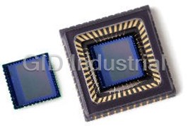
OMNI VISION OV5620
Description
OmniVision OV5620 Camera Chip Sensor with OmniPixel2 Technology - 5.17 mega-pixels, 1/25 lens size, optical black level calibration, defect pixel correction, high performance CMOS image sensor
Part Number
OV5620
Price
Request Quote
Manufacturer
OMNI VISION
Lead Time
Request Quote
Category
PRODUCTS - O
Specifications
array size
2592 x 1944
lens size
1/2.5?
max image transfer rate full
2592 x 1944 SXGA: 1280 x 960 D1: 720 x 480 VGA: 640 x 480
maximum system clock
48 MHz
output format
10-bit digital RGB Raw data
power supply analog
2.6 ~ 3.0V digital: 1.2V ± 5%
Features
- 50/60 Hz light auto detection
- defect pixel correction
- flash control output (strobe pin)
- high frame rate output mode
- horizontal and vertical sub-sampling for high frame rate with excellent image quality
- horizontal VarioPixel (binning) 1:2, 1:3, 1:4, 1:6
- image vertical flip/horizontal mirror
- internal/external frame synchronization
- on-chip luminance average counter
- optical black level calibration
- programmable image windowing
- programmable/auto exposure and gain control
- programmable/auto white balance control
- serial bus interface
- variable frame rate control
- vertical skip 1:2, 1:3, 1:4, 1:8
- vertical VarioPixel® (binning) 1:2, 1:3
- video or snapshot operations
Datasheet

Extracted Text
Advanced Information Preliminary Datasheet mni ision ® O TM OV5620 Color CMOS QSXGA (5.17 MPixel) CAMERACHIP Sensor TM with OmniPixel2 Technology General Description Applications • Digital still cameras The OV5620 (color) CAMERACHIP™ sensor is a high performance 5.17 mega-pixel CMOS image sensor for • Digital video cameras digital still image and video camera products. • PC camera/dual mode • Video conference equipment This device incorporates a 2592 x 1944 image array and an on-chip 10-bit A/D converter capable of operating at up Key Specifications to 7.5 frames per second (fps) in full resolution. The Array Size 2592 x 1944 OV5620 can also output 864 x 600 resolution at 60 fps Analog 2.6 ~ 3.0V enabling enhanced video viewing on TV. Proprietary Power Supply Digital 1.3V + 5% sensor technology utilizes advanced algorithms to cancel I/O 1.7 ~ 3.3V Fixed Pattern Noise (FPN), eliminate smearing, and Power Active 75 mA drastically reduce blooming, dark current and lens Requirements Standby 350 µA 1 T to 1/F shading. The control registers allow for flexible control of LINE Electronics Exposure where F = frame rate timing, polarity, and CAMERACHIP operation, which, in turn, Electronic rolling shutter, Shutter allows the engineer a great deal of freedom in product snapshot design. Output Format 10-bit digital RGB Raw data Lens Size 1/2.5" Lens Chief Ray Angle 12.5° Note: The OV5620 is available in a Input Clock 6 - 27 MHz Pb Pb lead-free package. Maximum System Clock 48 MHz Maximum Data Rate 48 MHz Full 7.5 fps 1.3Mpixel 30 fps Features Max Image D1MD 60 fps Transfer Rate • Optical black level calibration VGA 60 fps QVGA 120 fps • Video or snapshot operations Sensitivity 500 mV/(Lux • sec) • Programmable/Auto Exposure and Gain Control S/N Ratio 40 dB • Programmable/Auto White Balance Control Dynamic Range 54 dB • Horizontal and vertical sub-sampling for high frame Scan Mode Progressive rate with excellent image quality Pixel Size 2.2 µm x 2.2 µm Dark Current 3 mV/sec @ 60°C • High frame rate output mode Fixed Pattern Noise < 1% of V PEAK-TO-PEAK • Programmable image windowing Image Area 5.808 mm x 4.294 mm • Variable frame rate control Package Dimensions 14.22 mm x 14.22 mm • On-chip Luminance Average Counter Figure 1 OV5620 Pin Diagram (Top View) ® • VarioPixel (binning) 1:2, 1:3, 1:4 • Subsampling (skip) 1:2, 1:3, 1:4, 1:8 • Flash control output (strobe pin) • 50/60 Hz light auto detection 30 29 28 27 26 25 24 23 22 21 20 19 • Image vertical flip / horizontal mirror NC 31 18 NC 32 17 NC NC • Defect pixel correction DVDD 33 16 Y3 • Internal/External frame synchronization 34 15 Y4 Y2 Y5 35 14 Y1 • Serial bus interface 36 13 Y6 Y0 OV5620 • Power-on reset and power-down modes Y7 37 12 EXP_STB 38 11 Y8 RESET_B Y9 39 10 FREX Ordering Information 40 9 PCLK PWDN NC 41 8 NC 42 7 NC NC Product Package 43 44 45 46 46 48 1 2 3 4 5 6 OV05620-C03A (Color) CLCC-48 5620CLCC_DS_001 © 2007 OmniVision Technologies, Inc. VarioPixel, OmniVision, and the OmniVision logo are registered trademarks of OmniVision Technologies, Inc. Version 1.3, February 15, 2007 OmniPixel2 and CameraChip are trademarks of OmniVision Technologies, Inc. These specifications are subject to change without notice. VSYNC DGND HREF AVDD SCL DOGND SDA XVCLK SVDD PVDD AGND EGND DOVDD DATA_N STROBE DATA_P RVDD CLK_N VREF1 CLK_P VREF2 EVDD NC NC OV5620-CLCC Color CMOS QSXGA (5.17 MPixel) OmniPixel2™ CAMERACHIP™ Sensor Omni ision Functional Description Figure 2 shows the functional block diagram of the • 10-Bit A/D Converter OV5620 image sensor. The OV5620 includes: • Test Pattern Generator • Image Sensor Array (2592+16) x (1944+4) • Digital Signal Processor (DSP) resolution) • Snapshot (Frame Exposure) Mode Timing • Analog Amplifier • Frame Rate Adjust • Gain Control • SCCB Interface • Balance Control • Channel Average Calculator Figure 2 Functional Block Diagram column 10-bit Y[9:0] AMP digital sense amps A/D PCLK video port HREF (DVP) VSYNC image 50/60 Hz gain balance array buffer DSP* auto control control detect CP compact CN camera test port DP pattern (CCP) DN generator frequency timing generator control SCCB slave doubler and control logic register bank interface note 1 DSP* (white/black pixel correction, etc.) 5620CLCC_DS_002 Image Sensor Array Figure 3 Sensor Array Region Color Filter Layout columns The OV5620 sensor is a 1/2.5-inch CMOS imaging device. The sensor contains 5,174,400 pixels. Figure 3 shows the color filter layout. dummy 0 B G B G B G B G B G B G dummy 1 G R G R G R G R G R G R dummy The color filters are in a Bayer pattern. The primary color 2 B G B G B G B G B G B G 3 G R G R G R G R G R G R optical BG/GR array is arranged in line-alternating fashion. Of the 4 B G B G B G B G B G B G black 5,174,400 pixels, 5,080,384 are active. The other pixels dummy 5 G R G R G R G R G R G R dummy 6 B G B G B G B G B G B G are used for black level calibration and interpolation. dummy 7 G R G R G R G R G R G R 8 B G B G B G B G B G B G 1944 The sensor array design is based on a field integration active read-out system with line-by-line transfer and an lines 1951 G R G R G R G R G R G R electronic shutter with a synchronous pixel read-out 1952 B G B G B G B G B G B G 8 scheme. dummy lines 1959 G R G R G R G R G R G R 5620CLCC_DS_003 2 Proprietary to OmniVision Technologies, Inc. Version 1.3, February 15, 2007 row select XVCLK RESET_B PWDN FREX EXP_STB rows 0 1 2 3 4 5 SCL 2634 SDA 2635 2636 2637 2638 2639 Functional Description mni ision O Analog Amplifier Digital Signal Processor (DSP) • White/black pixel correction When the column sample/hold circuit has sampled one • Lens shading correction row of pixels, the pixel data will shift out one-by-one into an analog amplifier. Windowing Gain Control The OV5620 allows the user to define window size or region of interest (ROI), as required by the application. The amplifier gain can either be programmed by the user Window size setting (in pixels) ranges from 2x4 to or controlled by the internal automatic gain control circuit 2592 x 1944 (QSXGA) or 2 x 2 to 1280 x 960 (1.3 Mpixel) (AGC). The gain adjustment range is 0-24 dB. and 640 x 480 (VGA), and can be anywhere inside the 2592x1944 boundary. The windowing control merely alters the assertion of the HREF signal to be consistent Balance Control with the programmed horizontal and vertical ROI. Channel balance can be done manually by the user or by Figure 4 Windowing the internal automatic white balance (AWB) controller. column start column end HREF 10-Bit A/D Converter columns The balanced signal is then digitized by the on-chip 10-bit ADC. It can operate at up to 27 MHz and is fully synchronous to the pixel clock. The actual conversion rate row start is determined by the frame rate. display window row end Test Pattern Generator sensor array boundary The Test Pattern Generator features the following: 5620CLCC_DS_004 • 8-bar color bar pattern • Fade-to-gray color bar pattern • Shift "1" in output pin Version 1.3, February 15, 2007 Proprietary to OmniVision Technologies, Inc. 3 HREF rows OV5620-CLCC Color CMOS QSXGA (5.17 MPixel) OmniPixel2™ CAMERACHIP™ Sensor Omni ision Figure 9 Vertical 1:4 Average (Binning) VarioPixel (Binning) 1:2, 1:3, 1:4 Figure 5 Horizontal/Vertical 1:2 Average (Binning) B Gb B Gb B Gb B Gb B Gb B Gb B Gb B Gb B Gb Gr R Gr R Gr R Gr R Gr R Gr R Gr R Gr R Gr R B Gb B Gb B Gb B Gb B Gb B Gb B Gb B Gb B Gb B Gb B Gb Gr R Gr R Gr R Gr R Gr R Gr R Gr R Gr R Gr R Gr R Gr R B Gb B Gb B Gb B Gb B Gb B Gb B Gb B Gb B Gb B Gb Gr R Gr R Gr R Gr R Gr R Gr R Gr R Gr R Gr R B Gb B Gb Gr R B Gb B Gb B Gb B Gb B Gb B Gb B Gb B Gb B Gb Gr R Gr R Gr R Gr R Gr R Gr R Gr R Gr R Gr R Gr R Gr R 5620CLCC_DS_005 B Gb B Gb B Gb B Gb B Gb B Gb B Gb B Gb B Gb Gr R Gr R Gr R Gr R Gr R Gr R Gr R Gr R Gr R Figure 6 Horizontal 1:3 Average (Binning) B Gb B Gb B Gb B Gb B Gb B Gb B Gb B Gb B Gb Gr R Gr R Gr R Gr R Gr R Gr R Gr R Gr R Gr R B Gb B Gb B Gb B Gb B Gb B Gb B Gb B Gb B Gb Gr R Gr R Gr R Gr R Gr R Gr R Gr R Gr R Gr R B Gb B Gb B Gb B Gb B Gb B Gb B Gb B Gb B Gb B Gb B Gb B Gb B Gb Gr R Gr R Gr R Gr R Gr R Gr R Gr R Gr R Gr R Gr R Gr R Gr R Gr R 5620CLCC_DS_009 5620CLCC_DS_006 Flash Control Output (Strobe Pin) Figure 7 Vertical 1:3 Average (Binning) The OV5620 has a Strobe mode that allows it to work with an external flash and LED. B Gb Gr R Snapshot (Frame Exposure) Mode Timing B Gb The OV5620 supports snapshot (frame exposure) mode. Gr R Typically, the snapshot mode must work with the aid of an external shutter. B Gb B Gb Gr R Gr R The frame exposure pin, FREX (pin 10), is the snapshot mode enable pin and the EXP_STB pin (pin 12) serves as B Gb B Gb the sensor's exposure start trigger. When the external Gr R Gr R master device asserts the FREX pin high, the sensor array is quickly pre-charged and stays in reset mode until the B Gb EXP_STB pin is pulled low (sensor exposure time can be Gr R defined as the period between EXP_STB low to shutter close). After the FREX pin is pulled low, the video data B Gb stream is then clocked to the output port in a line-by-line Gr R manner. After completing one frame of data output, the 5620CLCC_DS_007 OV5620 will output continuous live video data unless in single frame transfer mode. Figure 17 shows detailed Figure 8 Horizontal 1:4 Average (Binning) timing of the Frame Exposure mode and Table 10 shows the timing specifications for this mode. When the OV5620 is working in snapshot mode, every B Gb B Gb B Gb B Gb B Gb B Gb B Gb B Gb B Gb line is sampled at different times causing different dark Gr R Gr R Gr R Gr R Gr R Gr R Gr R Gr R Gr R current levels line-by-line. To eliminate the dark current difference, the OV5620 provides line optical black pixel 5620CLCC_DS_008 output. The difference in dark current can be calibrated line-by-line. 4 Proprietary to OmniVision Technologies, Inc. Version 1.3, February 15, 2007 Functional Description mni ision O Figure 10 Slave Mode Connection Frame Rate Adjust The OV5620 offers four methods for frame rate Y[9:0] adjustment: RESET_B MHSYNC • Clock prescaler: (see “CLKRC” on page 17) PWDN MVSYNC By changing the system clock divide ratio, the frame rate and pixel rate will change together. This method XVCLK MCLK can be used for dividing the frame/pixel rate by: 1/2, master OV5620 1/3, 1/4 … 1/64 of the PLL output clock. device 5620CLCC_DS_010 • Horizontal blanking: (see “REG2A” on page 20 and see “EXHCL” on page 20) Figure 11 Slave Mode Timing By changing the horizontal blank timing in each line after active pixel output, the frame rate can be T frame changed while leaving the pixel rate as is. VSYNC • Vertical blanking: T VS By adding dummy line periods to the vertical sync T line T period (see “ADDVSL” on page 20 and “ADDVSH” HS HSYNC on page 20) or after the active lines (see “DMLNL” on page 21 and “DMLNH” on page 21), the frame rate T can be altered while the pixel rate remains the same. clk MCLK • PLL control: Supports more flexible clock control note 1 T > 6 T , T > T HS clk VS line note 2 T = 3252 x T (QSXGA); T = 1640 x T (1.3 Mpixel) line clk line clk SCCB Interface note 3 T = 1968 x T (QSXGA); T = 976 x T (1.3 Mpixel) frame line frame line 5620CLCC_DS_011 The OV5620 provides an on-chip SCCB serial control port that allows access to all internal registers, for complete control and monitoring of OV5620 operation. Channel Average Calculator Refer to OmniVision Technologies Serial Camera Control The OV5620 provides average output level data for Bus (SCCB) Specification for detailed usage of the serial frame-averaged luminance level. Access to the data is control port. provided via the SCCB interface. Slave Operation Mode Reset_B The OV5620 can be programmed to operate in slave The OV5620 includes a RESET_B pin (pin 11) that forces mode (default is master mode). a complete hardware reset when it is pulled low (ground). The OV5620 clears all registers and resets them to their When used as a slave device, the OV5620 re-uses input default values when a hardware reset occurs. A reset can pins, RESET_B and PWDN, for use as horizontal and also be initiated through the SCCB interface. vertical synchronization input triggers supplied by a master device. The master device must provide the following signals: Power Down Mode 1. System clock MCLK to XVCLK pin 2. Horizontal sync MHSYNC to RESET_B pin Two methods are available to place the OV5620 into power-down mode. 3. Vertical frame sync MVSYNC to PWDN pin • Hardware power-down may be selected by pulling the PWDN pin (pin 9) high (DOVDD). When this See Figure 10 for slave mode connections and Figure 11 occurs, the OV5620 internal device clock is halted for detailed timing considerations. and all internal counters are reset. The current draw is less than 250 µA in this standby mode. • Software power-down through the SCCB interface suspends internal circuit activity but does not halt the device clock. The current requirements drop to less than 1 mA in this mode. All register content is maintained in standby mode. Version 1.3, February 15, 2007 Proprietary to OmniVision Technologies, Inc. 5 OV5620-CLCC Color CMOS QSXGA (5.17 MPixel) OmniPixel2™ CAMERACHIP™ Sensor Omni ision Also, PCLK output can be programmed using register Digital Video Port COM10[5] to be gated by the active video period defined by the HREF signal. See Figure 13 for details. MSB/LSB Swap Figure 13 PCLK Output Only at Valid Pixels The OV5620 has a 10-bit digital video port. The MSB and PCLK LSB can be swapped with the control registers. Figure 12 PCLK active edge negative shows some examples of connections with external HREF devices. Figure 12 Connection Examples PCLK PCLK active edge positive MSB Y9 Y9 LSB Y9 Y0 VSYNC Y8 Y8 Y8 Y1 5620CLCC_DS_013 Y7 Y7 Y7 Y2 Y6 Y6 Y6 Y3 The specifications shown in Table 8 apply for Y5 Y5 Y5 Y4 DVDD = +1.3 V, DOVDD = +3.3 V, T = 25°C, sensor A Y4 Y4 Y4 Y5 working at 10 fps, external loading = 30 pF. Y3 Y3 Y3 Y6 Y2 Y2 Y2 Y7 Y1 Y1 Y1 Y8 Pixel Output Pattern LSB Y0 Y0 MSB Y0 Y9 external external OV5620 OV5620 Table 1 shows the output data order from the OV5620. device device The data output sequence following the first HREF and default 10-bit connection swap 10-bit connection after VSYNC is: B G B G … B G . 0,0 0,1 0,2 0,3 0,2590 0,2591 After the second HREF the output is G R G R … 1,0 1,1 1,2 1,3 MSB Y9 Y7 LSB Y9 G R …, etc. Y8 Y6 Y8 1,2590 1,2591 Y7 Y5 Y7 Y0 Y6 Y4 Y6 Y1 Table 1 Data Pattern Y5 Y3 Y5 Y2 Y4 Y2 Y4 Y3 R/C 0 1 2 3 . . . 2590 2591 Y3 Y1 Y3 Y4 0 B G B G . . . B G Y2 Y0 Y2 Y5 0,0 0,1 0,2 0,3 0,2590 0,2591 Y1 Y1 Y6 1 G R G R . . . G R 1,0 1,1 1,2 1,3 1,2590 1,2591 LSB Y0 MSB Y0 Y7 2 B G B G . . . B G external external 2,0 2 2,2 2,3 2,2590 2,2591 OV5620 OV5620 device device 3 G R G R . . . G R 3,0 3,1 3,2 3,3 3,2590 3,2591 default 8-bit connection swap 8-bit connection 5620CLCC_DS_012 . . . . 1942 B G B G B G 1942,0 1942,1 1942,2 1942,3 1942,2590 1942,2591 Line/Pixel Timing 1943 G R G R G R 1943,0 1943,1 1943,2 1943,3 1943,2590 1943,2591 The OV5620 digital video port can be programmed to work in either master or slave mode. In both master and slave modes, pixel data output is synchronous with PCLK (or MCLK if port is a slave), HREF, and VSYNC. The default PCLK edge for valid data is the negative edge but may be programmed using register COM10[4] for the positive edge. Basic line/pixel output timing and pixel timing specifications are shown in Figure 15 and Table 8. 6 Proprietary to OmniVision Technologies, Inc. Version 1.3, February 15, 2007 Pin Description mni ision O Pin Description Table 2 Pin Description Pin Number Name Pin Type Function/Description 01 DOVDD Power Power for I/O circuit (1.7V to 3.3V) 02 STROBE Output LED control output 03 RVDD Power Regulator power (2.8V) 04 VREF1 Analog Internal reference - connect to ground using a 0.1 µF capacitor 05 VREF2 Analog Internal reference - connect to ground using a 0.1 µF capacitor 06 NC – No connection 07 NC – No connection 08 NC – No connection 09 PWDN Input (0) Power down control, active high (hardware standby) 10 FREX Input (0) Frame exposure control 1 11 RESET_B Input (1) Hardware reset, active low 12 EXP_STB Input (0) Frame exposure control 2 13 Y0 Output Bit[0] of video output port 14 Y1 Output Bit[1] of video output port 15 Y2 Output Bit[2] of video output port 16 Y3 Output Bit[3] of video output port 17 NC – No connection 18 NC – No connection 19 NC – No connection 20 EVDD Power CCP2 power (2.8V) 21 CLK_P Output CCP2 positive clock output 22 CLK_N Output CCP2 negative clock output 23 DATA_P Output CCP2 interface positive data output 24 DATA_N Output CCP2 interface negative data output 25 EGND Power CCP2 ground 26 PVDD Power PLL power (2.8V) 27 XVCLK Input System clock input 28 DOGND Power Ground for I/O circuit 29 AVDD Power Analog power (2.8V) 30 DGND Power Digital ground 31 NC – No connection Version 1.3, February 15, 2007 Proprietary to OmniVision Technologies, Inc. 7 OV5620-CLCC Color CMOS QSXGA (5.17 MPixel) OmniPixel2™ CAMERACHIP™ Sensor Omni ision Table 2 Pin Description (Continued) Pin Number Name Pin Type Function/Description 32 NC – No connection Internal reference - connect to ground using a 0.1 µF capacitor or digital 33 DVDD Power power (1.3V) 34 Y4 Output Bit[4] of video output port 35 Y5 Output Bit[5] of video output port 36 Y6 Output Bit[6] of video output port 37 Y7 Output Bit[7] of video output port 38 Y8 Output Bit[8] of video output port 39 Y9 Output Bit[9] of video output port 40 PCLK Output Pixel clock output 41 NC – No connection 42 NC – No connection 43 VSYNC Output Vertical synchronization output 44 HREF Output Horizontal reference (data valid) output 45 SCL Input I2C clock 46 SDA I/O I2C data 47 SVDD Power Analog power (2.8V) 48 AGND Power Analog ground 8 Proprietary to OmniVision Technologies, Inc. Version 1.3, February 15, 2007 Electrical Characteristics mni ision O Electrical Characteristics Table 3 Operating Conditions Parameter Min Max Unit a Operating temperature -20 +70 °C Storage temperature -40 +125 °C a. Exceeding the stresses listed may permanently damage the device. This is a stress rating only and functional operation of the sensor at these and any other condition above those indicated in this specification is not implied. Exposure to absolute maximum rating conditions for any extended period may affect reliability. Table 4 DC Characteristics (-20°C < T < 70°C, Voltages referenced to GND) A Symbol Parameter Min Typ Max Unit Supply V Supply voltage (EVDD, PVDD, AVDD, SVDD) 2.6 2.8 3.0 V DD1 V Supply voltage (DOVDD) 1.7 2.8 3.3 V DD2 V Supply voltage (RVDD) 1.7 2.8 3.3 V DD3 a I Supply current (QSXGA at 7.5 fps) 45 (30 ) mA DD-VDD1 a I Supply current (QSXGA at 7.5 fps) 10 (35)mA DD-VDD2 a I Supply current (QSXGA at 7.5 fps) 20 (10)mA DD-VDD3 Digital Inputs V Input voltage LOW 0.3 x V V IL DD2 V Input voltage HIGH 0.7 x V V IH DD2 C Input capacitor 10 pF IN Digital Outputs V Output voltage HIGH 0.9 x V V OH DD2 V Output voltage LOW 0.1 x V V OL DD2 SCCB Inputs V SCL and SDA 0.3 x V V IL DD2 V SCL and SDA 0.7 x V V IH DD2 a. Number in parentheses represents current when CCP2 interface is used. Version 1.3, February 15, 2007 Proprietary to OmniVision Technologies, Inc. 9 OV5620-CLCC Color CMOS QSXGA (5.17 MPixel) OmniPixel2™ CAMERACHIP™ Sensor Omni ision Table 5 AC Characteristics (T = 25°C) A Symbol Parameter Min Typ Max Unit ADC Parameters B Analog bandwidth 24 27 MHz DLE DC differential linearity error 0.5 LSB ILE DC integral linearity error 1 LSB Settling time for hardware reset <1 ms Settling time for software reset <1 ms Settling time for 1.3 Mpixel/QSXGA mode change <1 ms Settling time for register setting <300 ms Table 6 Timing Characteristics Symbol Parameter Min Typ Max Unit Oscillator and Clock Input f Frequency (XVCLK) 6 24 27 MHz OSC t , t Clock input rise/fall time 2 ns r f Clock input duty cycle 45 50 55 % 10 Proprietary to OmniVision Technologies, Inc. Version 1.3, February 15, 2007 Timing Specifications mni ision O Timing Specifications Figure 14 Serial Bus Timing Diagram t t t F HIGH R SCL t t SU:STO LOW t t HD:STA SU:DAT SDA (IN) t SU:STA t t t AA HD:DAT BUF SDA (OUT) t DH 5620CLCC_DS_014 Table 7 Serial Bus Timing Specifications Symbol Parameter Min Typ Max Unit f Clock frequency 400 KHz SCL t Clock low period 1.3 µs LOW t Clock high period 600 ns HIGH t SCL low to data Out valid 100 900 ns AA t Bus free time before new START 1.3 µs BUF t START condition hold time 600 ns HD:STA t START condition setup time 600 ns SU:STA t Data-in hold time 0 µs HD:DAT t Data-in setup time 100 ns SU:DAT t STOP condition setup time 600 ns SU:STO t t Serial bus rise/fall times 300 ns R, F t Data-out hold time 50 ns DH Version 1.3, February 15, 2007 Proprietary to OmniVision Technologies, Inc. 11 OV5620-CLCC Color CMOS QSXGA (5.17 MPixel) OmniPixel2™ CAMERACHIP™ Sensor Omni ision Figure 15 QSXGA, 1.3 Mpixel, VGA and HF Mode Line/Pixel Output Timing t t p pr PCLK or MCLK t pf t t dphr dphf HREF t t dpd su invalid Y[9:0] P P P P P P 1279/2591 0 1 2 1078/2590 1279/2591 data t hd 5620CLCC_DS_015 Table 8 Pixel Timing Specification Symbol Parameter Min Typ Max Unit t PCLK period 20.83 ns p t PCLK rising time 4 ns pr t PCLK falling time 1 ns pf t PCLK negative edge to HREF rising edge 0 5 ns dphr t PCLK negative edge to HREF negative edge 0 5 ns dphf t PCLK negative edge to data output delay 0 5 ns dpd t Data bus setup time 15 ns su t Data bus hold time 8 ns hd 12 Proprietary to OmniVision Technologies, Inc. Version 1.3, February 15, 2007 Timing Specifications mni ision O Figure 16 Frame Timing T FRAME T VALID VSYNC 4 x T LINE V VB1 H H VB2 SYNC BLANK HREF HB1 HB2 HB1 HB2 note 1 T = T + V FRAME VALID BLANK note 2 H = HB1 + HB2 BLANK note 3 T = H + H LINE BLANK note 4 V = VB1 + VB2 + V BLANK SYNC 5620CLCC_DS_016 Table 9 Control Parameters for Standard Resolution Output H_Size V_Size H ( V Frame BLANK BLANK a b Format (pixels) (pixels) H_Bin V_Bin VB2 V VB1 HB1 HB2 pixels) (T ) Rate SYNC LINES (fps) 5 Mpixel 2592 1944 1:1 1:1 0 4 20 192 468 660 24 7.5 1.3 Mpixel 1280 960 1:2 1:2 0 4 13 192 168 360 17 30 D1MD 864 600 1:3 1:3 0 4 13 192 244 436 17 60 c QFMD 1280 480 1:2 1:4 0 4 13 192 140 332 17 60 d HF 1280 240 1:2 1:8 0 4 13 192 88 280 17 120 a. HB2 = H – HB1 BLANK b. Frame Rate listed is based on 48MHz internal system clock c. VGA (640x480) is derived from QFMD with 2:1 times skip/average in horizontal direction to get 60fps based on 24MHz PCLK (48MHz/2) d. QVGA (320x240) is derived from HF with 4:1 times skip/average in horizontal direction to get at 120fps based on 12MHz PCLK (48MHz/4) Version 1.3, February 15, 2007 Proprietary to OmniVision Technologies, Inc. 13 OV5620-CLCC Color CMOS QSXGA (5.17 MPixel) OmniPixel2™ CAMERACHIP™ Sensor Omni ision Figure 17 Snapshot Mode Timing with EXP_STB Asserted shutter open shutter FREX t def t des turn on flash EXP_STB t exposure time pre sensor sensor precharge timing t t dfvr dvsc t dfvf VSYNC t dvh HREF Y[9:0] row X row 0 row 1 row 1943 no following live video frame if set to transfer single frame 5620CLCC_DS_017 Table 10 Snapshot Timing Specifications Symbol Min Typ Max Unit tline 3252 (QSXGA) tp tdfvr 8 9 tp tdfvf 8 tline tdvsc 2tline tdvh 17 (QSXGA) tline tdhso 0 ns tdef 20 tp tdes 230 (QSXGA) tp NOTE 1) FREX must stay high long enough to ensure the entire sensor has been reset. 2) Shutter must be closed no later then 6000 tp after VSYNC falling edge. 14 Proprietary to OmniVision Technologies, Inc. Version 1.3, February 15, 2007 Register Set mni ision O Register Set Table 11 provides a list and description of the Device Control registers contained in the OV5620. The device slave addresses for the OV5620 are 60 for write and 61 for read. Table 11 Device Control Register List (Sheet 1 of 9) Address Register Default (Hex) Name (Hex) R/W Description AGC Gain Control Bit[7]: Reserved - must be set to "0" Bit[6:0]: Gain setting 00 GAIN 00 RW • Range: 1x to 16x Gain = (Bit[6]+1) x (Bit[5]+1) x (Bit[4]+1) x (1+Bit[3:0]/16) Note: Set COM8[2] = 0 to disable AGC. Digital AWB Blue Gain Control 01 BLUE 80 RW • Range: 0 to 4x ([00] to [FF]) Digital AWB Red Gain Control 02 RED 80 RW • Range: 0 to 4x ([00] to [FF]) Common Control 1 Bit[7:6]: Dummy frame control 00: Not used 01: Allow 1 dummy frame 03 COM1 4A RW 10: Allow 3 dummy frames 11: Allow 7 dummy frames Bit[5:4]: Reserved Bit[3:2]: Vertical window end line control 2 LSBs Bit[1:0]: Vertical window start line control 2 LSBs Register 04 Bit[7]: Horizontal mirror 04 REG04 00 RW Bit[6]: Vertical flip Bit[5:3]: Reserved Bit[2:0]: AEC lower 3 bits – AEC[2:0] 05-08 RSVD XX – Reserved Common Control 2 Bit[7:5]: Reserved Bit[4]: Sleep mode enable 0: Normal mode 1: Sleep mode Bit[3]: Reserved 09 COM2 01 RW Bit[2]: Pins PWDN and RESET_B used as SLVS and SLHS, respectively Bit[1:0]: Output drive current select 00: Weakest 01: Double capability 10: Double capability 11: Triple drive current 0A PIDH 56 R Product ID Number MSB (Read only) 0B PIDL 20 R Product ID Number LSB (Read only) Version 1.3, February 15, 2007 Proprietary to OmniVision Technologies, Inc. 15 OV5620-CLCC Color CMOS QSXGA (5.17 MPixel) OmniPixel2™ CAMERACHIP™ Sensor Omni ision Table 11 Device Control Register List (Sheet 2 of 9) Address Register Default R/W Description (Hex) Name (Hex) Common Control 3 Bit[7]: Array horizontal output size select 0: 1280, if COM4[7] = 1; 864, if COM4[0] = 1; otherwise, 2592 1: 1280, if in 1.3 Mpixel, QFMD, or HF mode; 864, if in D1MD mode; otherwise, 2592 Bit[6]: Array vertical skip mode select 0: Skip 2, if COM4[6] = 1; skip 3, if COM4[5] = 1; skip 4, if COM4[4] = 1; skip 8, if COM4[3] = 1; otherwise, no skip or full mode 1: Skip 2, if in 1.3 Mpixel mode; skip 3, if in D1MD mode; skip 4, if in QFMD mode; skip 8, if in HF mode; otherwise, no skip or full mode Bit[5:4]: Reserved Bit[3]: Number of vertical blanking line select 0: 24 lines, if in full mode; 16, if in 1.3 Mpixel, D1MD, QFMD, or HF mode 1: Full mode: DMLN > 24: determined by DMLN DMLN < 24: 24 lines 1.3 Mpixel/D1MD/QFMD/HF: DMLN > 16: determined by DMLN DMLN < 16: 16 lines Note: DMLN is set by registers {DMLNH[7:0] (0x47), DMLNL[7:0] 0C COM3 08 RW (0x46)} Bit[2]: Array vertical output size select 0: Full mode: 1944 1.3 Mpixel: 960 D1MD: 600 QFMD: 480 HF: 240 1: Output size determined by registers COM32[7:0] and COM30[5:4] Output size = 2 x {COM32[7:0], COM30[5:4]} Bit[1]: Number of horizontal blanking line select 0: Full mode: 660 1.3 Mpixel: 360 D1MD: 436 QFMD: 332 HF: 280 1: Determined by register EXHC[11:0] Note: EXCH[11:0] is set by registers {REG2A[7:4] (0x2A), EXHCL[7:0] (0x2B)} Bit[0]: Array horizontal output size select 0: Full mode: 1944 1.3 Mpixel: 960 D1MD: 600 QFMD: 480 HF: 240 1: Output size is determined by COM31[7:0] and COM30[2:0] Output size = 2 x {COM31[7:0], COM30[2:0]} 16 Proprietary to OmniVision Technologies, Inc. Version 1.3, February 15, 2007 Register Set mni ision O Table 11 Device Control Register List (Sheet 3 of 9) Address Register Default R/W Description (Hex) Name (Hex) Common Control 4 Bit[7:3]: Reserved Bit[2]: Clock output power-down pin status 0: Tri-state data output pin at power-down 1: Data output pin hold at last status before power-down 0D COM4 06 RW Bit[1]: Data output pin status selection at power-down 0: Tri-state data VSYNC, PCLK, HREF, and CHSYNC pins upon power-down 1: VSYNC, PCLK, HREF, and CHSYNC pins hold on last state before power-down Bit[0]: Reserved Common Control 5 0E COM5 01 RW Bit[7:0]: Reserved Common Control 6 Bit[7:2]: Reserved Bit[1]: Reset enable/disable when sensor working mode 0F COM6 43 RW changes 0: Sensor timing does not reset when mode changes 1: Sensor timing resets when mode changes Bit[0]: Reserved Automatic Exposure Control - AEC[10:3] 6 MSBs (AEC[16:11]) are in register REG45[5:0] and 3 LSBs (AEC[2:0]) are in register REG04[2:0]). AEC[16:0] - Exposure time 10 AEC 63 RW = t x AEC[16:0] T EX LINE Note: The maximum exposure time is 1 frame period even if T is EX longer than 1 frame period Clock Rate Control Bit[7]: Reserved Bit[6]: System clock divider enable 0: Clock from PLL output 11 CLKRC 00 RW 1: Enable system clock divider Bit[5:0]: Clock divider If CLKRC[5:0] = 0, then CLK = PLL CLK / 2 If CLKRC[5:0] ≠ 0, then CLK = PLL CLK / [(decimal value of CLKRC[5:0] + 1) x 2] Version 1.3, February 15, 2007 Proprietary to OmniVision Technologies, Inc. 17 OV5620-CLCC Color CMOS QSXGA (5.17 MPixel) OmniPixel2™ CAMERACHIP™ Sensor Omni ision Table 11 Device Control Register List (Sheet 4 of 9) Address Register Default R/W Description (Hex) Name (Hex) Common Control 7 Bit[7]: SRST 1: Initiates soft reset. All register are set to factory default values after which the chip resumes normal operation Bit[6:3]: Resolution selection 12 COM7 00 RW 0000: 5 Mpixel (full size) mode - no binning 0001: HF mode - 1:8 binning 0010: QFMD mode - 1:4 binning 0100: D1MD mode - 1:3 binning 1000: 1.3 Mpixel mode - 1:2 binning Bit[2:0]: Reserved Common Control 8 Bit[7]: AEC speed selection 0: Normal 1: Faster AEC correction Bit[6:3]: Reserved Bit[2]: AGC auto/manual control selection 0: Manual 13 COM8 C7 RW 1: Auto Bit[1]: AWB auto/manual control selection 0: Manual 1: Auto Bit[0]: Exposure control 0: Manual 1: Auto Common Control 9 Bit[7:5]: AGC gain ceiling 000: 2x 001: 4x 010: 8x 011: 16x 100: Reserved 101: Reserved 110: Reserved 111: Reserved 14 COM9 40 RW Bit[4:3]: Reserved Bit[2]: VSYNC drop option 0: VSYNC is always output 1: VSYNC is dropped if frame data is dropped Bit[1]: Frame data drop 0: Disable data drop 1: Drop frame data if exposure is not within tolerance. In AEC mode, data is normally dropped when data is out of range. Bit[0]: Reserved 18 Proprietary to OmniVision Technologies, Inc. Version 1.3, February 15, 2007 Register Set mni ision O Table 11 Device Control Register List (Sheet 5 of 9) Address Register Default R/W Description (Hex) Name (Hex) Common Control 10 Bit[7:6]: Reserved Bit[5]: PCLK output selection 0: PCLK always output 1: PCLK output qualified by HREF Bit[4]: PCLK edge selection 0: Data is updated at the failing edge of PCLK (user can latch data at the next rising edge of PCLK) 1: Data is updated at the rising edge of PCLK (user can latch data at the next falling edge of PCLK) Bit[3]: HREF output polarity 15 COM10 00 RW 0: Output positive HREF 1: Output negative HREF, HREF negative for valid data Bit2]: Reserved Bit[1]: VSYNC polarity 0: Positive 1: Negative Bit[0]: HSYNC polarity 0: Positive 1: Negative Digital AWB Green Gain Control 16 GREEN 80 RW • Range: 0 to 4x ([00] to [FF]) Horizontal Window Start 8 MSBs (3 LSBs in REG32[2:0]) 17 HREFST 12 RW Bit[10:0]: Select beginning of horizontal window, each LSB represents two pixels Horizontal Window End 8 MSBs (3 LSBs in REG32[5:3] B4 18 HREFEND RW Bit[10:0]: Select end of horizontal window, each LSB represents in 1.3 Mp two pixels Vertical Window Line Start 8 MSBs (2 LSBs in register COM1[1:0]) 01 19 VSTRT RW Bit[9:0]: Selects the start of the vertical window, each LSB in 1.3 Mp represents two scan lines. Vertical Window Line End 8 MSBs (2 LSBs in register COM1[3:2]) F4 1A VEND RW Bit[9:0]: Selects the end of the vertical window, each LSB in 1.3 Mp represents two scan lines. Pixel Shift Bit[7:0]: Pixel delay count - provides a method to fine tune the output timing of the pixel data relative to the HREF pulse. 1B PSHFT 00 RW It physically shifts the video data output time in units of pixel clock counts. The largest delay count is [FF] and is equal to 255 x PCLK. 1C MIDH 7F R Manufacturer ID Byte – High (Read only = 0x7F) 1D MIDL A2 R Manufacturer ID Byte – Low (Read only = 0xA2) 1E-23 RSVD XX – Reserved Version 1.3, February 15, 2007 Proprietary to OmniVision Technologies, Inc. 19 OV5620-CLCC Color CMOS QSXGA (5.17 MPixel) OmniPixel2™ CAMERACHIP™ Sensor Omni ision Table 11 Device Control Register List (Sheet 6 of 9) Address Register Default R/W Description (Hex) Name (Hex) Luminance Signal High Range for AEC/AGC operation 24 AEW 78 RW AEC/AGC value decreases in auto mode when average luminance is greater than AEW[7:0] Luminance Signal Low Range for AEC/AGC operation 25 AEB 68 RW AEC/AGC value increases in auto mode when average luminance is less than AEB[7:0] Fast Mode Large Step Range Thresholds - effective only in AEC/AGC fast mode Bit[7:4]: High threshold 26 VV D4 RW Bit[3:0]: Low threshold AEC/AGC may change in larger steps when luminance average is greater than VV[7:4] or less than VV[3:0] 27-29 RSVD XX – Reserved Register 2A Bit[7:4]: 4 MSBs of EXHC (8 LSBs in register EXHCL[7:0]) 2A REG2A 00 RW Bit[3:2]: HSYNC timing end point adjustment 2 MSBs Bit[1:0]: HSYNC timing start point adjustment 2 MSBs 8 LSBs of EXHC - pixel count in horizontal blank (valid only when 2B EXHCL 00 RW COM3[1] = 1) 2C RSVD XX – Reserved VSYNC Pulse Width 8 LSBs Bit[7:0]: Line periods added to VSYNC width. Default VSYNC 2D ADDVSL 00 RW . Each LSB count will add 1 x t output width is 4 x t line line to the VSYNC active period. VSYNC Pulse Width 8 MSBs Bit[7:0]: Line periods added to VSYNC width. Default VSYNC 2E ADDVSH 00 RW output width is 4 x t . Each MSB count will add line 256 x t to the VSYNC active period. line 2F YAVG 00 RW Luminance Average - this register will auto update HSYNC Position and Width Start 8 LSBs 30 HSDY 08 RW This register and register REG2A[1:0] define the HSYNC start position. Each LSB will shift HSYNC starting point by a 2 pixel period. HSYNC Position and Width End 8 LSBs 31 HEDY 30 RW This register and register REG2A[3:2] define the HSYNC end position. Each LSB will shift HSYNC end point by a 2 pixel period. Register 32 Bit[7:6]: Pixel clock divide option 00: No effect on PCLK 00 01: No effect on PCLK 32 REG32 RW in 1.3 Mp 10: PCLK frequency divide by 2 11: PCLK frequency divide by 4 Bit[5:3]: Horizontal window end position 3 LSBs Bit[2:0]: Horizontal window start position 3 LSBs 20 Proprietary to OmniVision Technologies, Inc. Version 1.3, February 15, 2007 Register Set mni ision O Table 11 Device Control Register List (Sheet 7 of 9) Address Register Default R/W Description (Hex) Name (Hex) 33-44 RSVD XX – Reserved Register 45 45 REG45 00 RW Bit[7:6]: AGC[9:8], AGC 2 MSBs Bit[5:0]: AEC[15:10], AEC 6 MSBs 46 DMLNL 00 RW Number of Vertical Blanking Lines LSBs 47 DMLNH 00 RW Number of Vertical Blanking Lines MSBs Common Control 19 Bit[7:2]: Reserved 48 ZOOMSL 00 RW Bit[1:0]: Zoom mode vertical start window 2 LSBs (see register ZOOMSH[7:0] (0x49) for 8 MSBs) 49 ZOOMSH 00 RW Zoom Mode Vertical Window Start Point 8 MSBs 4A-5E RSVD XX – Reserved Common Control 30 Bit[7:6]: Reserved Bit[5:4]: Array vertical output size (valid only when COM3[2] = 1) 5F COM30 00 RW Bit[3]: Reserved Bit[2:0]: Array hoizontal output size (valid only when COM3[0] = 1) Common Control 31 60 COM31 00 RW Bit[7:0]: Array horizontal output size (valid only when COM3[0] = 1) Common Control 32 61 COM32 00 RW Bit[7:0]: Array vertical output size (valid only when COM3[2] = 1) 62 RSVD XX – Reserved Common Control 34 Bit[7]: Reserved Bit[6]: De-noise enable 0: Disable 63 COM34 00 RW 1: Enable Bit[5]: Strength of de-noise select 0: DNSTH x 1 1: DNSTH x 4 Bit[4:0]: De-noise threshold setting 64-7F RSVD XX – Reserved Version 1.3, February 15, 2007 Proprietary to OmniVision Technologies, Inc. 21 OV5620-CLCC Color CMOS QSXGA (5.17 MPixel) OmniPixel2™ CAMERACHIP™ Sensor Omni ision Table 11 Device Control Register List (Sheet 8 of 9) Address Register Default R/W Description (Hex) Name (Hex) DSP Function Enable Control Bit[7:5]: Reserved Bit[4]: Color bar enable 0: Disable 1: Enable Bit[3:2]: Reserved 80 DSPEN 01 RW Bit[1]: Raw data output select 0: Raw data after CIP 1: Raw data before CIP Bit[0]: New CIP enable 0: Disable 1: Enable DSP01 Bit[7:4]: Reserved Bit[3]: WBC delay option when DSP01[1] and DSP01[2] are disabled 0: Do not delay 1: Delay output Bit[2]: Black pixel canceling enable 81 DSP01 00 RW 0: Disable 1: Enable Bit[1]: White pixel canceling enable 0: Disable 1: Enable Bit[0]: White and black pixel canceling enable 0: Disable 1: Enable 82 RSVD XX – Reserved Digital Gain Control Bit[7:2]: Reserved Bit[1:0]: Digital gain select 83 DGCTRL 80 RW 00: 1x 01: 2x 10: 4x 11: 4x 84 AWBBIAS 00 RW AWB Gain Bias Setting DSP Control 85 DSPCTRL 00 RW Bit[7:0]: Reserved 86-88 RSVD XX – Reserved DSP09 Bit[7:6]: Reserved Bit[5]: AWB gain enable 89 DSP09 29 RW 0: Disable 1: Enable Bit[4:0]: Reserved 22 Proprietary to OmniVision Technologies, Inc. Version 1.3, February 15, 2007 Register Set mni ision O Table 11 Device Control Register List (Sheet 9 of 9) Address Register Default R/W Description (Hex) Name (Hex) 8A RSVD XX – Reserved DSP0B Bit[7:6]: Reserved Bit[5]: Gamma enable 8B DSP0B 1F RW 0: Disable 1: Enable Bit[4:0]: Reserved 8C-A7 RSVD XX – Reserved A8 BOTLMT 10 RW Pixel Value Lower Limit A9 TOPLMT F0 RW Pixel Value Upper Limit AA-B7 RSVD XX – Reserved Red Gain Limit Bit[7:4]: Red gain upper limit B8 REDLMT F0 RW Value = bit[7:4] x 16 + 15 Bit[3:0]: Red gain lower limit Value = bit[3:0] x 16 Green Gain Limit Bit[7:4]: Green gain upper limit B9 GREENLMT F0 RW Value = bit[7:4] x 16 + 15 Bit[3:0]: Green gain lower limit Value = bit[3:0] x 16 Blue Gain Limit Bit[7:4]: Blue gain upper limit BA BLUELMT F0 RW Value = bit[7:4] x 16 + 15 Bit[3:0]: Blue gain lower limit Value = bit[3:0] x 16 BB-F6 RSVD XX – Reserved NOTE: All other registers are factory-reserved. Please contact OmniVision Technologies for reference register settings. Version 1.3, February 15, 2007 Proprietary to OmniVision Technologies, Inc. 23 OV5620-CLCC Color CMOS QSXGA (5.17 MPixel) OmniPixel2™ CAMERACHIP™ Sensor Omni ision Package Specifications The OV5620 uses a 48-pin ceramic package. Refer to Figure 18 for package information and Figure 19 for the array center on the chip. Figure 18 OV5620 Package Specifications .560 SQ +.012/-.005 .464 SQ ±.005 .440 ±.005 .418 SQ ±.005 .06 +.010/-.005 .088 ±.009 .040 ±.003 .065 ±.007 42 31 31 42 .030 ±.002 glass .015 ±.002 43 30 30 43 42 31 .020 ±.002 43 30 .040 TYP .018 .022 ±.002 MIN .001 to .005 TYP die .002 ±.001 TYP 48 48 48 .535 ±.004 1 .029 ±.001 1 1 .038 ±.007 pin 1 index pin 1 index image 6 19 plane .020 TYP 7 18 619 19 6 .012 TYP REF 7 18 18 7 R .0075 R .0075 .085 TYP (4 corners) (48 plcs) note 1 all exposed metallized areas shall be gold-plated 0.50 μm min. thk. over nickel plate unless otherwise specified in purchase order. note 2 seal area and die attach area shall be without metallization. 5620CLCC_DS_018 Table 12 OV5620 Package Dimensions Dimensions Millimeters (mm) Inches (in.) Package size 14.22 +0.30 / -0.13 SQ .560 +.012 / -.005 SQ Package height 2.23 + 0.28 .088 + .011 Substrate base height 0.51 + 0.05 .020 + .002 Cavity size 10.62 + 0.13 SQ .418 + .005 SQ Castellation height 1.14 + 0.14 .045 + .006 Pin #1 pad size 0.51 x 2.16 .020 x .085 Pad size 0.51 x 1.02 .020 x .040 Pad pitch 1.02 + 0.18 .040 + .003 Package edge to first lead center 1.52 +0.26 / -0.13 .06 +.010 / -.005 End-to-end pad center-center 11.18 + 0.13 .440 + .005 Glass size 13.6 + 0.1 SQ .535 + .004 SQ Glass height 0.55 + 0.05 .022 + .002 Die thickness 0.733 + 0.015 .029 + .001 Top of glass to image plane 0.95 + 0.18 .037 + .007 Substrate height 1.65 + 0.18 .065 + .007 24 Proprietary to OmniVision Technologies, Inc. Version 1.3, February 15, 2007 Package Specifications mni ision O Sensor Array Center Figure 19 OV5620 Sensor Array Center 5808 μm package center (0 μm, 0 μm) 4294.4 μm array center (23.2 μm, -464.4 μm) sensor (0.913 mil, -18.283 mils) array die package pin 1 positional die shift (x,y) = 0.15 mm (6 mils) max. tolerances die tilt = 0.75 degrees max. die rotation = 3 degrees max. note1 this drawing is not to scale and is for reference only. note2 as most optical assemblies invert and mirror the image, the chip is typically mounted with pin 1 (DOVDD) oriented down as shown. 5620CLCC_DS_019 The recommended lens chief ray angle for the OV5620 is 12.5° degrees. Version 1.3, February 15, 2007 Proprietary to OmniVision Technologies, Inc. 25 OV5620-CLCC Color CMOS QSXGA (5.17 MPixel) OmniPixel2™ CAMERACHIP™ Sensor Omni ision IR Reflow Ramp Rate Requirements OV5620 Lead-Free Packaged Devices Note: For OVT devices that are lead-free, all part marking letters are lower case. Figure 20 IR Reflow Ramp Rate Requirements 300.0 Z1 Z2 Z3 Z4 Z5 Z6 Z7 end 275.0 250.0 225.0 200.0 175.0 150.0 125.0 100.0 75.0 50.0 25.0 0.0 time (sec) 5620CLCC_DS_020 Table 13 Reflow Conditions Condition Exposure Average ramp-up rate (30°C to 217°C) Less than 3°C per second > 100°C Between 330 - 600 seconds > 150°C At least 210 seconds > 217°C At least 30 seconds (30 ~ 120 seconds) Peak temperature 245°C Cool-down rate (peak to 50°C) Less than 6°C per second Time from 30°C to 245°C No greater than 390 seconds 26 Proprietary to OmniVision Technologies, Inc. Version 1.3, February 15, 2007 temperature (°C) -22 -2 18 38 58 78 98 118 138 158 178 198 218 238 258 278 298 318 338 358 369 Package Specifications mni ision O Note: • All information shown herein is current as of the revision and publication date. Please refer to the OmniVision web site (http://www.ovt.com) to obtain the current versions of all documentation. • OmniVision Technologies, Inc. reserves the right to make changes to their products or to discontinue any product or service without further notice (It is advisable to obtain current product documentation prior to placing orders). • Reproduction of information in OmniVision product documentation and specifications is permissible only if reproduction is without alteration and is accompanied by all associated warranties, conditions, limitations and notices. In such cases, OmniVision is not responsible or liable for any information reproduced. • This document is provided with no warranties whatsoever, including any warranty of merchantability, non-infringement, fitness for any particular purpose, or any warranty otherwise arising out of any proposal, specification or sample. Furthermore, OmniVision Technologies Inc. disclaims all liability, including liability for infringement of any proprietary rights, relating to use of information in this document. No license, expressed or implied, by estoppels or otherwise, to any intellectual property rights is granted herein. • ‘OmniVision’, ‘VarioPixel’, and the OmniVision logo are registered trademarks of OmniVision Technologies, Inc. ‘CameraChip’ and ’OmniPixel2’ are trademarks of OmniVision Technologies, Inc. All other trade, product or service names referenced in this release may be trademarks or registered trademarks of their respective holders. Third-party brands, names, and trademarks are the property of their respective owners. For further information, please feel free to contact OmniVision at info@ovt.com. OmniVision Technologies, Inc. 1341 Orleans Drive Sunnyvale, CA USA (408) 542-3000 Version 1.3, February 15, 2007 Proprietary to OmniVision Technologies, Inc. 27 OV5620-CLCC Color CMOS QSXGA (5.17 MPixel) OmniPixel2™ CAMERACHIP™ Sensor Omni ision 28 Proprietary to OmniVision Technologies, Inc. Version 1.3, February 15, 2007 mni isionTM O REVISION CHANGE LIST Document Title: OV5620 (CLCC) Datasheet Version: 1.0 DESCRIPTION OF CHANGES • Initial Release mni isionTM O REVISION CHANGE LIST Document Title: OV5620 (CLCC) Datasheet Version: 1.1 DESCRIPTION OF CHANGES The following changes were made to version 1.0: ® • Under Features on page 1, deleted (previously 11th) bulleted item “Vertical VarioPixel (binning) 1:2, 1:3 ® • Under Featuress on page 1, changed 10th bulleted item from “Horizontal VarioPixel ® (binning) 1:2, 1:3, 1:4, 1:8” to “VarioPixel (binning) 1:2, 1:3, 1:4” • Under Features on page 1, changed 11th bulleted item from “Vertical skip 1:2, 1:3, 1:4, 1:8” to “Subsampling (skip) 1:2, 1:3, 1:4, 1:8” • Moved section title “Horizontal VarioPixel/Binning 1:2, 1:3” to page 4 and changed it to “VarioPixel (Binning) 1:2, 1:3, 1:4” • On page 4, deleted section title “Vertical VarioPixel/Binning 1:2, 1:3” • On page 4, deleted “Horizontal 1:2 Skip” figure (previously Figure 8) • Under General Description on page 1, changed the second line in the second paragraph from “...can also output 864 x 648 ...” to “...can also output 864 x 600 ...” • Under Key Specifications on page 1, changed Digital Power Supply specification from “1.2V + 5%” to “1.3V + 5%” • Under Key Specifications on page 1, changed Standby Power Requirements from “<10 µA” to “250 µA” • Under Key Specifications on page 1, corrected Shutter specification from “Electronic rolling shutter, snapshort” to “Electronic rolling shutter, snapshot” • Under Key Specifications on page 1, changed specification for Lens Chief Ray Angle from “TBD” to “12.5°” • Under Key Specifications on page 1, changed Max Image Transfer Rate parameter from “SXGA” to “1.3 Mpixel”, from “D1” to “D1MD”, and from “HF” to “QVGA” • In Figure 1 on page 1, changed OV5620 chip so that pin 1 is down • Under Gain Control subsection on page 3, changed the last line from “The gain adjustment range 0-42 dB” to “The gain adjustment range is 0-24 dB” • On page 4, deleted section title “Vertical Skip 1:2, 1:3, 1:4, 1:8” • On page 4, deleted “Vertical 1:2 Skip” figure (previously Figure 9), “Vertical 1:3 Skip” figure (previously Figure 10), “Vertical 1:4 Skip” figure (previously Figure 11), and “Vertical 1:8 Skip” figure (previously Figure 12) • On page 4, added Figure 8 “Horizontal 1:4 Average (Binning)” and Figure 9 “Vertical 1:4 Average (Binning)” • Under Frame Rate Adjust on page 5, changed first line from “The OV5620 offers three methods ...” to “The OV5620 offers four methods ...” mni isionTM O DESCRIPTION OF CHANGES (CONTINUED) • Under Frame Rate Adjust on page 5, changed the last line of the first bulleted item from “... of the input clock rate” to “... of the PLL output clock” • Under Frame Rate Adjust on page 5, changed first line of the second bulleted item from “By adding a dummy pixel timing in ...” to “By changing horizontal blank timing in ...” • Under Frame Rate Adjust on page 5, added “... or after the active lines (see “DMLNL” on page 21 and “DMLNH” on page 21”)” to first line of third bulleted item • Under Frame Rate Adjust on page 5, added a fourth bulleted item of “PLL control: Supports more flexible clock control” • In the Notes for Figure 10 on page 5, changed note 2 from “ T = 3000 x T (QSXGA); line clk T = 1632 x T (SXGA)” to “T = 3252 x T (QSXGA); T = 1640 x T (1.3 line clk line clk line clk Mpixel)” • In the Notes for Figure 10 on page 5, changed note 3 from “T = 2000 x T (QSXGA); T = 980 x T (SXGA)” to frame line frame line “T = 1968 x T (QSXGA); T = 976 x T (1.3 Mpixel)” frame line frame line • Under Power Down Mode on page 5, changed first line of the first bulleted item from “... high (+3.3VDC)...” to “... high (DOVDD)...” • Under Power Down Mode on page 5, changed last line of the second bulleted item from “The current draw is less than 10 µA in this standby mode” to “The current draw is less than 250 µA in this standby mode” • In Line/Pixel Timing section on page 6, changed the last paragraph from “The specification shown in Table 8 apply for DVDD = +1.2 V, ...” to “The specification shown in Table 8 apply for DVDD = +1.3 V, ...” • In Table 2 on page 7, changed description of pin 1 from “Power for I/O circuit (1.8V to 3.3V)” to “Power for I/O circuit (1.7V to 3.3V)” • In Table 2 on page 7, deleted “(1.8V to 3.3V)” from the description of pin 28 • In Table 2 on page 8, changed description of pin 33 from “... or digital power (1.2V)” to “... or digital power (1.3V)” • In Table 4 on page 9, changed Min, Typ, and Max for Supply voltage (DVDD) (V ) DD3 from “1.14”, “1.2”, and “1.26” to “1.24”, “1.3”, and “1.37”, respectively • In Figure 16 on page 13, added callout for V and changed Note 4 SYNC • In Table 9 on page 13, added columns for VB2, V , VB1, HB1, and HB2 SYNC • In Table 9 on page 13, changed Formats “XGA” and “AFMD” to “1.3Mpixel” and “HF”, respectively • In Table 9 on page 13, changed Frame Rate of HF (previously AFMD) from “60” to “120” • In Figure 17 on page 14, deleted “t ” dhv • In Table 10 on page 14, deleted rows for “tvs” and “tdhv” • In Table 10 on page 14, changed Typ for tline from “3000 (QSXGA)” to “3252 (QSXGA)” • In Table 10 on page 14, deleted Max for tdfvf and added Typ spec of “8” mni isionTM O DESCRIPTION OF CHANGES (CONTINUED) • In Table 10 on page 14, changed Typ for tdvh from “18268 (QSXGA)” to “17 (QSXGA)” and changed Unit from “tp” to “tline” • In Table 10 on page 14, changed Max for tdes from “2500 (QSXGA)” to “230 (QSXGA)” • In Table 11 on page 15. changed description of register GAIN (0x00) from: AGC Gain Control Bit[7:0]: Gain setting • Range: 1x to 32x Gain = (Bit[7]+1) x (Bit[6]+1) x (Bit[5]+1) x (Bit[4]+1) x (1+Bit[3:0]/16) Note: Set COM8[2] = 0 to disable AGC. to: AGC Gain Control Bit[7]: Reserved - must be set to “0” Bit[6:0]: Gain setting • Range: 1x to 16x Gain = (Bit[6]+1) x (Bit[5]+1) x (Bit[4]+1) x (1+Bit[3:0]/16) Note: Set COM8[2] = 0 to disable AGC. • In Table 11 on page 15, changed description of register BLUE (0x01) from “Range: 0 to 4x ([00] to [44])” to “Range: 0 to 4x ([00] to [FF])” • In Table 11 on page 15, changed description of register RED (0x02) from “Range: 0 to 4x ([00] to [44])” to “Range: 0 to 4x ([00] to [FF])” • In Table 11 on page 16, changed description for register bit COM3[7] from: Bit[7]: Array horizontal output size select (excluding crop mode) to: Bit[7]: Array horizontal output size select • In Table 11 on page 16, changed description for register bit COM3[6] from: Bit[6]: Array vertical skip mode select (excluding crop mode) 0: Skip 2 (output size = 960), if COM4[6] = 1; skip 3 (output size = 600), if COM4[5] = 1; skip 4 (output size = 480), if COM4[4] = 1; skip 8 (output size = 240), if COM4[3] = 1; otherwise, no skip or full mode (output size = 1944) 1: Skip 2 (output size = 960), if in XGA mode; skip 3 (output size = 600), if in D1MD mode; skip 4 (output size = 480), if in QFMD mode; skip 8 (output size = 240), if in AFMD mode; otherwise, no skip or full mode (output size = 1944) to: Bit[6]: Array vertical skip mode select 0: Skip 2, if COM4[6] = 1; skip 3, if COM4[5] = 1; skip 4, if COM4[4] = 1; skip 8, if COM4[3] = 1; otherwise, no skip or full mode 1: Skip 2, if in 1.3 Mpixel mode; skip 3, if in D1MD mode; skip 4, if in QFMD mode; skip 8, if in HF mode; otherwise, no skip or full mode mni isionTM O DESCRIPTION OF CHANGES (CONTINUED) • In Table 11 on page 16, changed description for register bit COM3[3] from: Bit[3]: Number of vertical blanking line select (excluding crop mode) 0: 24 lines, if in full mode; 16, if in XGA, D1MD, QFMD, or AFMD mode 1: 24 lines, if in full mode; less than 24lines, if register DMLN is less than 24; otherwise, number of blanking lines is determined by register DMLN 16 lines, if in XGA, D1MD, QFMD, or AFMD mode; less than 16 lines, if register DMLN is less than 16; otherwise, number of blanking lines is determined by DMLN to: Bit[3]: Number of vertical blanking line select 0: 24 lines, if in full mode; 16, if in 1.3 Mpixel, D1MD, QFMD, or HF mode 1: Full mode: DMLN > 24: determined by DMLN DMLN < 24: 24 lines 1.3Mpixel/D1MD/QFMD/HF: DMLN > 16: determined by DMLN DMLN < 16: 16 lines • In Table 11 on page 16, changed description for register bit COM3[2] from: Bit[2]: Array vertical output size select (excluding crop mode) 0: 1944, if in full mode; 960, if in XGA mode; 600, if in D1MD mode; 480, if in QFMD mode; 240, if in AFMD mode 1: Output size determined by registers COM32[7:0] and COM30[5:4] Output size = 2 x {COM32[7:0], COM30[5:4]} to: Bit[2]: Array vertical output size select 0: Full mode: 1944 1.3 Mpixel: 960 D1MD: 600 QFMD: 480 HF: 240 1: Output size determined by registers COM32[7:0] and COM30[5:4] Output size = 2 x {COM32[7:0], COM30[5:4]} • In Table 11 on page 16, changed description for register bit COM3[1] from: Bit[1]: Number of horizontal blanking line select (excluding crop mode) 0: 660, if in full mode; 360, if in XGA mode; 436, if in D1MD mode; 280, if in AFMD mode 1: Determined by register EXHC[11:0] to: Bit[1]: Number of horizontal blanking line select 0: Full mode: 660 1.3 Mpixel: 360 D1MD: 436 QFMD: 332 HF: 280 1: Determined by register EXHC[11:0] mni isionTM O DESCRIPTION OF CHANGES (CONTINUED) • In Table 11 on page 16, changed description for register bit COM3[0] from: Bit[0]: Array horizontal output size select (excluding crop mode) 0: 1944, if in full mode; 960, if in XGA mode; 600, if in D1MD mode; 480, if in QFMD mode; 240, if in AFMD mode 1: Output size is determined by COM31[7:0] and COM30[2:0] Output size = 2 x {COM31[7:0], COM30[2:0]} to: Bit[0]: Array horizontal output size select 0: Full mode: 1944 1.3 Mpixel: 960 D1MD: 600 QFMD: 480 HF: 240 1: Output size is determined by COM31[7:0] and COM30[2:0] Output size = 2 x {COM31[7:0], COM30[2:0]} • In Table 11 on page 18, changed description of register bits COM9[7:5] (0x14) from: Bit[7:5]: AGC gain ceiling 000: 2x 001: 4x 010: 8x 011: 16x 100: 32x 101: Reserved 110: Reserved 111: Reserved to: Bit[7:5]: AGC gain ceiling 000: 2x 001: 4x 010: 8x 011: 16x 100: Reserved 101: Reserved 110: Reserved 111: Reserved • In Table 11 on page 20, added “- pixel count in horizontal blank valid only when Reg0C[1] = 1” to description of register EXHCL (0x2B) • In Table 11 on page 20, changed description for register ADDVSL[7:0] from: VSYNC Pulse Width 8 LSBs Bit[7:0]: Line periods added to VSYNC width. Default VSYNC output width is 2 x t . Each LSB count will line add 1 x t to the VSYNC active period. line to: VSYNC Pulse Width 8 LSBs Bit[7:0]: Line periods added to VSYNC width. Default VSYNC output width is 4 x t . Each LSB count will line add 1 x t to the VSYNC active period. line • In Table 11 on page 21, deleted row for register ZOOMW (0x34) • In Table 11 on page 21, changed addresses for RSVD from “35-44” to “34-44” • In Table 11 on page 22, changed description of register bit DSPEN[7] (0x80) to “Reserved” • In Table 11 on page 23, changed address for RSVD row from “BB-DF” to “BB-F6” • In Table 11 on page 23, deleted rows for registers E0 to F6 • In Figure 19 on page 25, changed orientation of OV5620 chip so pin 1 is down mni isionTM O REVISION CHANGE LIST Document Title: OV5620 (CLCC) Datasheet Version: 1.2 DESCRIPTION OF CHANGES The following changes were made to version 1.1: • Under Key Specifications on page 1, changed specification for Active Power Requirements from “TBD” to “75 mA” • Under Key Specifications on page 1, changed specification for Standby Power Requirements from “250 µA” to “350 µA” • In Table 4 on page 9, changed description of V from “Supply voltage (RVDD, EVDD, DD1 PVDD, AVDD, SVDD)” to “Supply voltage (EVDD, PVDD, AVDD, SVDD)” • In Table 4 on page 9, changed description of V from “Supply voltage (DVDD)” to DD3 “Supply voltage (RVDD)” • In Table 4 on page 9, changed Min, Typ, and Max for V from “1.24”, “1.3”, and DD3 “1.37” to “1.7”, “2.8”, and “3.3”, respectively • In Table 4 on page 9, changed Typ for V , V , and V from “TBD”, “TBD”, and DD1 DD2 DD3 a a a “TBD” to “45 (30 )”, “10 (35 )”, and “20 (10 )”, respectively • In Table 4 on page 9, added table footnote “a” mni isionTM O REVISION CHANGE LIST Document Title: OV5620 (CLCC) Datasheet Version: 1.3 DESCRIPTION OF CHANGES The following changes were made to version 1.2: • Under Key Specifications on page 1, changed specification for Dark Current from “TBD” to “3 mV/sec @ 60°C” • Under Key Specifications on page 1, changed specification for Fixed Pattern Noise from “TBD” to “< 1% of V ” PEAK-TO-PEAK
Frequently asked questions
What makes Elite.Parts unique?

What kind of warranty will the OV5620 have?
Which carriers does Elite.Parts work with?
Will Elite.Parts sell to me even though I live outside the USA?
I have a preferred payment method. Will Elite.Parts accept it?
Why buy from GID?

Quality
We are industry veterans who take pride in our work

Protection
Avoid the dangers of risky trading in the gray market

Access
Our network of suppliers is ready and at your disposal

Savings
Maintain legacy systems to prevent costly downtime

Speed
Time is of the essence, and we are respectful of yours
Related Products

USB 2.0 FLEX MODULE EVEAL KIT
OV02630-VL7A PROTOTYPING MO
USB 2.0 EVAL MODULE W/LIERA
MODULE
2 MPIXEL CAMERA CHIP-ROHS 1/4" LENS, 38 PIN CSP2 - NPA
OVT USB 2.0 EVAL BOARD W/OV3620-C00SENSOR (1BOARD
Request a Quote

The quote request has been received
Close

Facing challenges or have inquiries? Feel free to contact us!
Call Us +1-469-283-2440
What they say about us
FANTASTIC RESOURCE
One of our top priorities is maintaining our business with precision, and we are constantly looking for affiliates that can help us achieve our goal. With the aid of GID Industrial, our obsolete product management has never been more efficient. They have been a great resource to our company, and have quickly become a go-to supplier on our list!
Bucher Emhart Glass
EXCELLENT SERVICE
With our strict fundamentals and high expectations, we were surprised when we came across GID Industrial and their competitive pricing. When we approached them with our issue, they were incredibly confident in being able to provide us with a seamless solution at the best price for us. GID Industrial quickly understood our needs and provided us with excellent service, as well as fully tested product to ensure what we received would be the right fit for our company.
Fuji
HARD TO FIND A BETTER PROVIDER
Our company provides services to aid in the manufacture of technological products, such as semiconductors and flat panel displays, and often searching for distributors of obsolete product we require can waste time and money. Finding GID Industrial proved to be a great asset to our company, with cost effective solutions and superior knowledge on all of their materials, it’d be hard to find a better provider of obsolete or hard to find products.
Applied Materials
CONSISTENTLY DELIVERS QUALITY SOLUTIONS
Over the years, the equipment used in our company becomes discontinued, but they’re still of great use to us and our customers. Once these products are no longer available through the manufacturer, finding a reliable, quick supplier is a necessity, and luckily for us, GID Industrial has provided the most trustworthy, quality solutions to our obsolete component needs.
Nidec Vamco
TERRIFIC RESOURCE
This company has been a terrific help to us (I work for Trican Well Service) in sourcing the Micron Ram Memory we needed for our Siemens computers. Great service! And great pricing! I know when the product is shipping and when it will arrive, all the way through the ordering process.
Trican Well Service
GO TO SOURCE
When I can't find an obsolete part, I first call GID and they'll come up with my parts every time. Great customer service and follow up as well. Scott emails me from time to time to touch base and see if we're having trouble finding something.....which is often with our 25 yr old equipment.
ConAgra Foods