

 Manufacturers
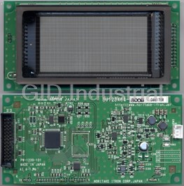
NORITAKE GU128X64-800B
Description
Noritake GU128X64-800B Dot Graphic Module, 140.0 x 68.0 PCB Size, 83.05 x 41.45 Display Area, 5V / 700 mA Typical Power, with 700 cd/m² Brightness, 8 bit parallel and CMOS synchronous serial Interface
Part Number
GU128X64-800B
Price
Request Quote
Manufacturer
NORITAKE
Lead Time
Request Quote
Category
VFD/LCD DISPLAYS
Specifications
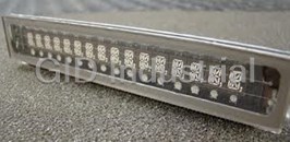
Color of illumination
Green (Blue Green)
Display area
83.05 mm x 41.45 mm (X x Y)
Dot pitch
0.65 mm x 0.65 mm (X x Y)
Dot size
0.5 mm x 0.5 mm (X x Y)
Luminance
350cd/m2 (Min.)
Datasheet

Extracted Text
RoHS 2002/95/EC
Vacuum Fluorescent Display
Module Specification
Model: GU128X64-800B
Specification No: DS-1239-0000-03
Date of Issue: May 19, 2005
Revision: May 1, 2006
December 20, 2007
January 23, 2008
:
:
PUBLISHED BY
NORITAKE ITRON CORP. / JAPAN
This specification is subject to change without prior notice.
This product complies with RoHS Directive 2002/95/EC
GU128X64-800B
Table of Contents
1. General Description ................................................................................................................................................2
2. Absolute Maximum Ratings ...................................................................................................................................2
3. Electrical Characteristics .......................................................................................................................................2
4. Optical Specifications.............................................................................................................................................2
5. Environmental Specifications ................................................................................................................................2
6. Description of Bus and Signals .............................................................................................................................3
6.1 Parallel Interface ...........................................................................................................................................3
6.2 Serial Interface ..............................................................................................................................................3
7. Block Diagram.........................................................................................................................................................3
8. Display Screen and Initialize Set ...........................................................................................................................4
8.1 Graphic Display (GRAM)...............................................................................................................................5
9. Function...................................................................................................................................................................7
9.1 Commands ....................................................................................................................................................7
9.2 Display On/Off (C/D= "1")..............................................................................................................................8
9.3 Brightness Set (C/D= "1")..............................................................................................................................8
9.4 Display Clear (C/D= "1") This command clears the GRAM. .........................................................................9
9.5 Display Area Set (C/D="1", only used for Initialize Set) ...............................................................................10
9.6 GRAM Data Write position Address Set (Graphic Display) (C/D="1")..........................................................11
9.6.1 GRAM Data Write Position X Address Set ............................................................................................11
9.6.2 GRAM Data Write Position Y Address Set ............................................................................................11
9.7 GRAM Display Start Position Address Set (C/D="1") .................................................................................11
9.7.1 Horizontal Shift......................................................................................................................................11
9.7.2 Vertical Shift ..........................................................................................................................................11
9.8 Address Mode Set(C/D="1") ..................................................................................................................12
9.9 Address Read (C/D ="1").......................................................................................................................12
9.10 Data Write to Graphic Display(GRAM) (C/D="0") ......................................................................................13
9.11 Default Status at Reset ..............................................................................................................................14
9.12 FRP (Frame Pulse)..................................................................................................................................14
10. Interface ................................................................................................................................................................15
10.1 Parallel Interface (Parallel #1) ...................................................................................................................15
10.1.1 Command Write operation ..................................................................................................................15
10.1.2 Command Read operation .................................................................................................................15
10.1.3 Data Write operation ...........................................................................................................................15
10.2 Parallel Interface(Parallel #2) ....................................................................................................................16
10.2.1 Command Write operation ..................................................................................................................16
10.2.2 Command Read operation ..................................................................................................................16
10.2.3 Data Write operation ...........................................................................................................................16
10.3 Serial Interface ..........................................................................................................................................17
10.3.1 Timing .................................................................................................................................................17
11. Jumper ..................................................................................................................................................................18
11.1 Jumper Position.........................................................................................................................................18
11.2 Jumper Setting (Must be done when power is OFF)................................................................................18
12. Pin Assignment (See connector diagrams below) ..............................................................................................19
12.1 Signal Connection .....................................................................................................................................19
12.2 Connectors ...............................................................................................................................................19
13. Outline Dimension ..............................................................................................................................................20
1
GU128X64-800B
1. General Description
1.1 Construction: A 128X64 dot BD-VFD single board display module consisting of an 8 bit
micro-computer, and a DC/DC converter.
1.2 Features: Simultaneous display of graphic.
Flexible Display and Editing Functions.
Compact design due to the application of a BD-VFD tube.
1.3 Dimensions: See attached drawings.
2. Absolute Maximum Ratings
Parameter SymbolMin.Typ.Max. Unit Condition
Logic Input Voltage VI -0.5 - Vcc +0.3 V -
Power Supply Voltage Vcc 0 - 6.5 VDC -
3. Electrical Characteristics
Measurement Conditions: 25°C / Vcc=5.0V
Parameter SymbolMin.Typ.Max.Unit Condition
"H" VIH 4.0 - - IIH= 2μA
Logic Input Voltage VDC
"L" VIL - - 1.0 IIL= ‐600μA
"H" VOH 4.7 - - IOH=‐300μA
Logic Output Voltage VDC
"L" VOL - - 0.3 IOL= 300μA
"H" VRH 4.0 - - VDC IRH= 5μA
Reset Input Voltage
"L" VRL - - 0.6 VDC IRL= ‐600μA
Power Supply Voltage Vcc 4.75 5.00 5.25 VDC -
- 0.70 0.90 VCC=+5V, All dots ON
Power Supply Current Icc A
- 0.55 0.75 VCC=+5V, All dots OFF
Notes:
The rise time of Vcc should not exceed 100 ms.
Icc may peak at power up may be more than twice the normal operating current
4. Optical Specifications
Number of dots: 8192 (128X64)
Display area: 83.05 mm x 41.45 mm (X x Y)
Dot size: 0.5 mm x 0.5 mm (X x Y)
Dot pitch: 0.65 mm x 0.65 mm (X x Y)
2
Luminance: 350cd/m (Min.)
Color of illumination: Green (Blue Green)
5. Environmental Specifications
Operating temperature: -40 to +85°C
Storage temperature: -40 to +85°C
Storage humidity: 20 to 80 % R.H(Non Condensation)
Vibration: 10-55-10Hz, all amplitude 1mm, 30Min., X-Y-Z (Non operating)
2
Shock: 539m/s 10mS (Non operating)
2
GU128X64-800B
6. Description of Bus and Signals
This module has serial and 2 types of parallel interface.
Type of interface can be selected by jumper settings. Refer to 11 on page # 18 for details.
6.1 Parallel Interface
Data Line Function
D0 ~ D7
Data Bus (Input / Output)
WR (R/W) Parallel #1: Write Signal, Parallel #2: R/W (Input)
RD (ENCK) Parallel #1: Read Signal, Parallel #2: ENCK (Input)
CSS
Chip Select (Input)
C/D Command / Data Select Signal (Input)
C/D = "1" … Command C/D = "0" … Data
FRP Frame Pulse Signal (Output)
RESET="0"… Reset (Input)
RESET
Vcc Power Supply
GND Ground
6.2 Serial Interface
Data Line Function
RXD Serial Input
TXD Serial Output
SCK
Clock (Input)
CSS Chip Select (Input)
C/D Command / Data Select Signal (Input)
C/D = "1" … Command C/D = "0" … Data
FRP Frame Pulse Signal (Output)
RESET="0"… Reset (Input) Active Low
RESET
Vcc Power Supply
GND Ground
7. Block Diagram
():Parallel#2
~
D0 D7
RD(ENCK)
Controller
WR(R/W)
Parallel
C/D
CSS
Display Data
FRP
Writing Signal
RESET
RXD
TXD
Scan Control
BD-VFD
Detection Signal
SCK
Serial
C/D
Graphic Protection
CSS
Operation
Circuit
RAM
FRP
Detection Signal
RESET
Filament(AC)
Vcc
DC/DC
Anode & Grid(DC)
Converter
GND
3
GU128X64-800B
8. Display Screen and Initialize Set
The Display screen consists of 8,192 dots arranged as 128 by 64 dots. It is divided into 64 display area blocks of 16 by
8 dots each. Each display area block can be assigned to GRAM (Graphic mode) or DDRAM (Character mode) by the
Display Area Set command. (9.5 Page #10)
But, this is the version which has no Font ROM. Therefore, DDRAM is not available, all of display area block must
be assigned to GRAM as the initialize setting, and this must be done when the module is powered up and also
every time the reset is applied, because all display area blocks are set to DDRAM area as default setting.
Initialize sequence is as follows;
Initialize Set Start
Display Clear
C/D=1 5FHex
Wait 1mS
n=0
C/D=1 62Hex
C/D=1 0nHex
Data Write
C/D=0 FFHex
n=n+1
NO
n=8?
YES
END
4
GU128X64-800B
8.1 Graphic Display (GRAM)
GRAM consists of 16,384 bits arranged in 128 by 128 bit blocks with access is structured as 8 bits
of vertical data. The detail of GRAM is as follows:
GRAM Data Write Position Address
X-Address
00・・・・・・ ・・・・・・・・ ・・・・・・・・ ・・・・・・・・ 7FH
D0
0H
D1
1H
D2
D3
2H
D4
3H
D5
0H
D6 4H
D7
1H
5H
2H
6H
3H
7H
Y-Address
8H
9H
AH
BH
CH
DH
EH
FH
GRAM Data Write
128bit
Position Address
(0H - FH)
5
64bit
128bit
GU128X64-800B
8.1 Cont’d
GRAM Display Start Position Address
X-Address
00・・・・・・ ・・・・・・・・ ・・・・・・・・ ・・・・・・・・ 7FH
00H
D0
07H
D1 08H
0FH
D2
10H
D3
17H
D4 18H
1FH
GRAM
D5
20H
Layer 0(X=00H, Y=00H)
0H
D6
27H
28H
D7
1H
2FH
30H
2H
37H
38H
3H
3FH
Y-Address
40H
47H
48H
4FH
50H
57H
58H
5FH
GRAM
60H
Layer1(X=00H, Y=00H)
67H
68H
6FH
70H
77H
78H
7FH
128bit
GRAM Display Start
Position Address
(00H - 7FH)
This module has 2 layers - Layer 0 and Layer 1. Each layer in this display consists of 128 by 64 dots.
Display merging using these 2 layers can be done with the Display ON/OFF command. Refer to 9.2
on page # 8 for details.
Layer 0 has an area of 128x64 dots that starts from top left point defined by the GRAM Start Position
Address. The area of Layer 1 is the next 128x64 dots.
When the value of the GRAM Start Position Address X overflow = 7FH, the next position goes to 00H.
When the value of the GRAM Start Position Address Y overflow = 7FH, the next position goes to 00H.
For example:
If the GRAM Start Position Address is set as X=02H, Y=08H, the area of Layer 0 is as follows;
X=02H,03H,04H……7FH,00H,01H
Y=08H,09H…………46H, 47H
In this case, the area of Layer1 is as follows;
X=02H,03H,04H……7FH,00H,01H
Y=48H,49H…………06H,07H
6
64bit
128bit
GU128X64-800B
9. Function
9.1 Commands
D7 D6 D5 D4 D3 D2 D1 D0 Comments
Command C/D
0 0 1 0 L1 L0 * * 1st Byte Display ON/OFF
Display
1
EXO Control、
ON/OFF
0 GS 0 GRV AND * * 2nd Byte
R
2 Byte Command
Brightness
1 0 1 0 0 BW3 BW2 BW1 BW0 1 Byte 1 Byte Command
Set
Display
1 0 1 0 1 G1C G0C 1 HM 1 Byte 1 Byte Command
Clear
Display 0 1 1 0 0 0 1 0 1st Byte Display Area is
1
Area SET 0 0 0 0 0 (A2 – A0) 2nd Byte assigned
(Initialize) 3 Byte Command
0 1 1 1 1 1 1 1 1 3rd Byte
0 1 1 0 0 1 0 * 1st Byte Graphic Display
1
Data Write X-Address Set, 2 Byte
GRAM X-Address (GXA6~GXA0) 2nd Byte
Position Command
Address
Graphic Address
0 1 1 0 0 0 0 * 1st Byte
Set
1 Y-Address Set, 2-Byte
* * * * GYA3GYA2GYA1GYA0 2nd Byte
Command
Graphic Display
0 1 1 1 * * * * 1st Byte
Display
1
Horizontal Shift, 2-Byte
Start
XA7 XA6 XA5 XA4 XA3 XA2 XA1 XA0 2nd Byte
Command
Position
Graphic Display
Address
1 1 0 1 1 UD S1 S0 * 1 Byte Vertical
Set
Shift, 1 Byte Command
Address Address Increment, 1
1 1 0 0 0 * IGX IGY * 1 Byte
Mode Set Byte Command
1 1 0 1 0 1 * * 1st Byte Graphic Display
(GRAM) Horizontal
Address
1 * VG6 VG5 VG4 VG3 VG2 VG1 VG0 2nd Byte And Vertical Display
Read
Start Address, 3 Byte
HG7 HG6 HG5 HG4 HG3 HG2 HG1 HG0 3rd Byte Command
Writes Data
Data Write 0 WRITE DATA
Graphic Data is 1 Byte
* Either a “0” or a “1” is acceptable
7
GU128X64-800B
9.2 Display On/Off (C/D= "1")
The GRAM Layer is selected with the 1st Byte of data. DDRAM (On/Off), GRAM (On/Off), DDRAM
(reverse or normal modes), GRAM (reverse or normal modes) and display merge are selected by
the 2nd Byte. Reverse mode toggles the representation of green in the foreground and black in the
background to the exact opposite - green to back and black to the foreground. This is similar to the
concept of reverse video.
1st Byte:
MSB LSB
0 0 1 0 L1 L0 * * * Either a “0” or a “1” is acceptable
< --------------------------- > < --------- >
Command Select Display Control Data
L1= (1 OR 0) = GRAM Layer 1 (Active OR Inactive)
L0= (1 OR 0) = GRAM Layer 0 (Active OR Inactive)
2nd Byte:
MSB LSB
0 GS 0 GRV AND EXOR * * * Either a “0” or a “1” is acceptable
< --------------------------- ------------------- >
Display Control Data
GS= (1 OR 0) Graphic Display Area (GRAM) = (On OR Off)
GRV= (1 OR 0) Graphic Display Area (GRAM) = (Reverse OR Normal)
DS=”0”, GS= “0”: Stand-by mode
1st Byte 2nd Byte
Action
L1 L0 AND EXOR
* * 1 * AND Display of Layer 1& 0
* * 0 1 EXOR Display of Layer 1& 0
1 1 0 0 OR Display of Layer 1& 0
1 0 0 0 Only Layer1 selected for display
0 1 0 0 Only Layer0 selected for display
0 0 0 0 Graphic Display Off
* Either a “0” or a “1” is acceptable
9.3 Brightness Set (C/D= "1")
The Brightness level of the display screen can be scaled by the following four bit control.
Please note that the brightness is consistent across the illuminated pixels. There is no scaling of
individual pixels. The display self-initializes to 100% brightness.
MSB LSB
0 1 0 0 BW3BW2BW1BW0
< --------------------------- > < ---------------------------- >
Command Select Brightness Level Data
8
GU128X64-800B
9.3 Cont’d
Brightness levels are set by the following:
BW3 BW2 BW1 BW0 Brightness Level
0 0 0 0 100%(Light)
0 0 0 1 94%
0 0 1 0 87%
0 0 1 1 81%
0 1 0 0 75%
0 1 0 1 69%
0 1 1 0 62%
0 1 1 1 56%
1 0 0 0 50%
1 0 0 1 44%
1 0 1 0 37%
1 0 1 1 31%
1 1 0 0 25%
1 1 0 1 19%
1 1 1 0 12%
1 1 1 1 6%(Dark)
9.4 Display Clear (C/D= "1") This command clears the GRAM.
This command should always be applied at power on or reset. In the period of 1mS following the
issue of this command, the module requires internal processing and does not accept any
commands.
MSB LSB
0 1 0 1 G1CG0C 1 HM
< --------------------------- > < ---------------------------- >
Command Select Clear Control Code
To clear the GRAM area, G1C or G0C bit must be asserted. By asserting HM bit, both data write position
address and display start position address which selected by G1C, G0C, DC also be reset.
HM = (1 or 0) equals (Initialize data write position address and display start position address or Not initialize).
G1C= (1 or 0) equals (GRAM area 1 is cleared or GRAM area 1 not cleared)
G0C= (1 or 0) equals (GRAM area 0 cleared or GRAM area 0 not cleared)
GRAM area 1: X= 00H-7FH, Y=0H – 7H (Display data write position address)
GRAM area 2: X= 00H-7FH, Y=8H – FH (Display data write position address)
9
GU128X64-800B
9.5 Display Area Set (C/D="1", only used for Initialize Set)
This command sets the display area block as Graphic Display (GRAM) or Character display
(DDRAM). But, this is version which has no Font ROM. Therefore, DDRAM is not available, all of
display area block must be assigned to GRAM as the initialize setting, and this must be done when
the module is powered up and also every time the reset is applied. Setup is performed by 3-byte
command.
1st Byte: (C/D="1") Command Select
MSB LSB
0 1 1 0 0 0 1 0
< ------------------------------------------------------------ >
Command Select
2nd Byte: (C/D="1") Display Area Data Address Select
MSB LSB
0 0 0 0 0 A2 A1 A0 (0H – 7H)
< ------------------ >
Display Area Data Address
3rd Byte: (C/D="0") Display Area Block Select
MSB LSB
1 1 1 1 1 1 1 1
< ------------------------------------------------------------- >
Display Data
D0 to D7 = "1": Graphic Display (GRAM)
D0 to D7 = "0": Character Display (DDRAM, Not available)
Display area block is assigned as follows on a screen.
8dot
D0 D4 D0 D4 D0 D4 D0 D4 D0 D4 D0 D4 D0 D4 D0 D4
16 dot
D1 D5 D1 D5 D1 D5 D1 D5 D1 D5 D1 D5 D1 D5 D1 D5
D2 D6 D2 D6 D2 D6 D2 D6 D2 D6 D2 D6 D2 D6 D2 D6
D3 D7 D3 D7 D3 D7 D3 D7 D3 D7 D3 D7 D3 D7 D3 D7
0 34 5 6
12 7
Display Area Data Address (0to7H)
10
GU128X64-800B
9.6 GRAM Data Write position Address Set (Graphic Display) (C/D="1")
This command specifies both X & Y data write position address.
9.6.1 GRAM Data Write Position X Address Set
Data write position X address of GRAM expressed with 8 bits (00Hex-7FHex) is specified.
Refer to 8.1 Graphic Display (GRAM) on Page #5.
1st Byte: Command Select
MSB LSB
* Either a “0” or a “1” is acceptable
0 1 1 0 0 1 0 *
< ------------------------------------------------------------- >
2nd Byte: GRAM Data Write Position X Address
MSB LSB
0 GXA6 GXA5 GXA4 GXA3 GXA2 GXA1 GXA0
< ------------------------------------------------------------- >
9.6.2 GRAM Data Write Position Y Address Set
Data write position Y address of GRAM expressed with 4 bits (0Hex-FHex) is specified.
1st Byte:
MSB LSB
* Either a “0” or a “1” is acceptable
0 1 1 0 0 0 0 *
< -------------------------------------------------------------- >
Command Select
2nd Byte:
MSB LSB
* * * * GYA3 GYA2 GYA1 GYA0 * Either a “0” or a “1” is acceptable
< -------------------------- >
9.7 GRAM Display Start Position Address Set (C/D="1")
9.7.1 Horizontal Shift
This command specifies the address that a display pattern can be positioned to by 8 bits (00Hex
to 7FHex). This is equivalent to an offset in the X-axis.
1st Byte:
MSB LSB
* Either a “0” or a “1” is acceptable
0 1 1 1 * * * *
< --------------------------- >
Command Select
2nd Byte:
MSB LSB
XA7 XA6 XA5 XA4 XA3 XA2 XA1 XA0
< -------------------------------------------------------------- >
GRAM Display Start Position Address
9.7.2 Vertical Shift
This is equivalent to an offset Y-axis.
MSB LSB
* Either a “0” or a “1” is acceptable
1 0 1 1 UD S1 S0 *
< --------------------------- > < ------------------ >
Command Select Display Shift Data
UD= "1": Display scrolled up.
UD= "0": Display scrolled down.
S1= "0", S0= "1": Display shift by 8 dots.
S1= "1", S0= "0": Display shift by 1 dot.
S1= "1", S0= "1": Display shift by 2 dots.
11
GU128X64-800B
9.8 Address Mode Set(C/D="1")
This command specifies the GRAM data write position address auto increment mode.
MSB LSB
* Either a “0” or a “1” is acceptable
1 0 0 0 * IGX IGY *
< --------------------------- > < ---------------- >
Command Select Address Mode data
IGX = "1" : X-Address +1(increment) when writing to GRAM.(It not affect to Y-Address.)
IGX = "0" : GRAM X address fixed mode
IGY = "1" : Y-Address +1(increment) when writing to GRAM.(It not affect to X-Address
IGY = "0" : GRAM Y address fixed mode.
9.9 Address Read (C/D ="1")
This command reads both vertical and horizontal display start position addresses of GRAM (Refer to sect. 8 -
Display Screen and Initialize set on Page # 4). On the parallel interface, the data bus outputs the address until CSS
goes high after the READY signal goes active (Parallel #1:RD=LOW, Parallel #2:R/W=HIGH). The Data bus
becomes an input when other. On the serial interface, TXD outputs the data from SCK rising after command is
issued until the CSS goes high. Refer to 10.Interface on Page #15.
1st Byte:
MSB LSB
* Either a “0” or a “1” is acceptable
1 1 0 1 0 1 * *
< --------------------------- >
Command Select
MSB LSB
2nd Byte: * VG6 VG5 VG4 VG3 VG2 VG1 VG0 (Read)
3rd Byte: HG7 HG6 HG5 HG4 HG3 HG2 HG1 HG0 (Read)
< -------------------------------------------------------------- >
Vertical & Horizontal display start position address (GRAM)
VG0 to VG6: Vertical display start position address
HG0 to HG7: Horizontal display start position address
12
GU128X64-800B
9.10 Data Write to Graphic Display(GRAM) (C/D="0")
Can be written into GRAM by setting GRAM X or Y data write position address.
Example:
Writing "EA Hex" sets "D1, 3, 5, 6, 7 =1" and "D0, 2, 4 =0".
Display
Input Data
D0
D1
D2
D3
D4
D5
D6
D7
: Display ON
13
1 1 1 0 1 0 1 0
GU128X64-800B
9.11 Default Status at Reset
When the reset is applied, the display self-initializes into the following status:
GRAM Layer: Layer ( 0 )
Display ON/OFF: Display ( Off )
Display Area: All DDRAM (Character display area)
All of display area block must be assigned to GRAM again as the initialize setting after
reset is applied because DDRAM is not available.
GRAM X-address: Fixed mode
GRAM Y-address: Fixed mode
Brightness Level: 100% Brightness
The following precautions should be observed at power on, and after a reset:
External Reset: After Vcc reaches 2.5V, the Reset level is "Low" for more than 1.5mS.
Power-Up: The following sequence occurs:
Data receive
V CC≧2.5V
Min 1. 5ms
V <0.3V
CC
0
Frequently asked questions
What makes Elite.Parts unique?

What kind of warranty will the GU128X64-800B have?
Which carriers does Elite.Parts work with?
Will Elite.Parts sell to me even though I live outside the USA?
I have a preferred payment method. Will Elite.Parts accept it?
Why buy from GID?

Quality
We are industry veterans who take pride in our work

Protection
Avoid the dangers of risky trading in the gray market

Access
Our network of suppliers is ready and at your disposal

Savings
Maintain legacy systems to prevent costly downtime

Speed
Time is of the essence, and we are respectful of yours
Related Products
Request a Quote

The quote request has been received
Close

Facing challenges or have inquiries? Feel free to contact us!
Call Us +1-469-283-2440
What they say about us
FANTASTIC RESOURCE
One of our top priorities is maintaining our business with precision, and we are constantly looking for affiliates that can help us achieve our goal. With the aid of GID Industrial, our obsolete product management has never been more efficient. They have been a great resource to our company, and have quickly become a go-to supplier on our list!
Bucher Emhart Glass
EXCELLENT SERVICE
With our strict fundamentals and high expectations, we were surprised when we came across GID Industrial and their competitive pricing. When we approached them with our issue, they were incredibly confident in being able to provide us with a seamless solution at the best price for us. GID Industrial quickly understood our needs and provided us with excellent service, as well as fully tested product to ensure what we received would be the right fit for our company.
Fuji
HARD TO FIND A BETTER PROVIDER
Our company provides services to aid in the manufacture of technological products, such as semiconductors and flat panel displays, and often searching for distributors of obsolete product we require can waste time and money. Finding GID Industrial proved to be a great asset to our company, with cost effective solutions and superior knowledge on all of their materials, it’d be hard to find a better provider of obsolete or hard to find products.
Applied Materials
CONSISTENTLY DELIVERS QUALITY SOLUTIONS
Over the years, the equipment used in our company becomes discontinued, but they’re still of great use to us and our customers. Once these products are no longer available through the manufacturer, finding a reliable, quick supplier is a necessity, and luckily for us, GID Industrial has provided the most trustworthy, quality solutions to our obsolete component needs.
Nidec Vamco
TERRIFIC RESOURCE
This company has been a terrific help to us (I work for Trican Well Service) in sourcing the Micron Ram Memory we needed for our Siemens computers. Great service! And great pricing! I know when the product is shipping and when it will arrive, all the way through the ordering process.
Trican Well Service
GO TO SOURCE
When I can't find an obsolete part, I first call GID and they'll come up with my parts every time. Great customer service and follow up as well. Scott emails me from time to time to touch base and see if we're having trouble finding something.....which is often with our 25 yr old equipment.
ConAgra Foods