

 Manufacturers
KONTRON KIT-FMC-DEV
Description
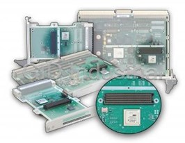
Kontron KIT-FMC-DEV VITA57 FMC Development Kit
Part Number
KIT-FMC-DEV
Price
Request Quote
Manufacturer
KONTRON
Lead Time
Request Quote
Category
PRODUCTS - K
Features
- Available for x86 and Power PC architectures
- Immediate start into VITA 57 based designs
Datasheet

Extracted Text
VITA 57 Development Kit User's Guide SD.DT.F79-0e - May 2011 If it's embedded, it's Kontron. Development Kit User's Guidede Preface Revision History Publication Title: Development Kit User's Guidede Doc. ID: SD.DT.F79-0e Rev. Brief Description of Changes Date of Issue 0e Initial Version May 2011 Copyright © 2011 Kontron AG. All rights reserved. All data is for information purposes only and not guaranteed for legal purposes. Information has been carefully checked and is believed to be accurate; however, no responsibility is assumed for inaccuracies. Kontron and the Kontron logo and all other trademarks or registered trademarks are the property of their respective owners and are recognized. Specifications are subject to change without notice. Page i SD.DT.F79-0e Development Kit User's Guidede Preface Proprietary Note This document contains information proprietary to Kontron. It may not be copied or transmitted by any means, disclosed to others, or stored in any retrieval system or media without the prior written consent of Kontron or one of its authorized agents. The information contained in this document is, to the best of our knowledge, entirely correct. However, Kontron cannot accept liability for any inaccuracies or the consequences thereof, or for any liability arising from the use or application of any circuit, product, or example shown in this document. Kontron reserves the right to change, modify, or improve this document or the product described herein, as seen fit by Kontron without further notice. Trademarks This document may include names, company logos and trademarks, which are registered trademarks and, therefore, proprietary to their respective owners. Environmental Protection Statement This product has been manufactured to satisfy environmental protection requirements where possible. Many of the components used (structural parts, printed circuit boards, connectors, batteries, etc.) are capable of being recycled. Final disposition of this product after its service life must be accomplished in accordance with applicable country, state, or local laws or regulations. The Waste Electrical and Electronic Equipment (WEEE) Directive aims to: > reduce waste arising from electrical and electronic equipment (EEE) > make producers of EEE responsible for the environmental impact of their products, especially when they become waste > encourage separate collection and subsequent treatment, reuse, recovery, recycling and sound environmental disposal of EEE > improve the environmental performance of all those involved during the lifecycle of EEE SD.DT.F79-0e Page ii Development Kit User's Guidede Preface Conventions This guide uses several types of notice: Note, Caution, ESD. Note: this notice calls attention to important features or instructions. Caution: this notice alert you to system damage, loss of data, or risk of personal injury. ESD: This banner indicates an Electrostatic Sensitive Device. All numbers are expressed in decimal, except addresses and memory or register data, which are expressed in hexadecimal. The prefix `0x' shows a hexadecimal number, following the `C' programming language convention. 3 6 9 The multipliers `k', `M' and `G' have their conventional scientific and engineering meanings of *10 , *10 and *10 respectively. The only exception to this is in the description of the size of memory areas, when `K', `M' and `G' 10 20 30 mean *2 , *2 and *2 respectively. 3 6 9 10 20 30 When describing transfer rates, `k' `M' and `G' mean *10 , *10 and *10 not *2 *2 and *2 . In PowerPC terminology, multiple bit fields are numbered from 0 to n, where 0 is the MSB and n is the LSB. PCI and CompactPCI terminology follows the more familiar convention that bit 0 is the LSB and n is the MSB. Signal names ending with an asterisk (*) or a hash (#) denote active low signals; all other signals are active high. Signal names follow the PICMG 2.0 R3.0 CompactPCI Specification and the PCI Local Bus 2.3 Specification. For Your Safety Your new Kontron product was developed and tested carefully to provide all features necessary to ensure its compliance with electrical safety requirements. It was also designed for a long fault-free life. However, the life expectancy of your product can be drastically reduced by improper treatment during unpacking and installation. Therefore, in the interest of your own safety and of the correct operation of your new Kontron product, you are requested to conform with the following guidelines. High Voltage Safety Instructions Warning! All operations on this device must be carried out by sufficiently skilled personnel only. Caution, Electric Shock! Before installing a not hot-swappable Kontron product into a system always ensure that your mains power is switched off. This applies also to the installation of piggybacks. Serious electrical shock hazards can exist during all installation, repair and maintenance operations with this product. Therefore, always unplug the power cable and any other cables which provide external voltages before performing work. Page iii SD.DT.F79-0e Development Kit User's Guidede Preface Special Handling and Unpacking Instructions ESD Sensitive Device! Electronic boards and their components are sensitive to static electricity. Therefore, care must be taken during all handling operations and inspections of this product, in order to ensure product integrity at all times Do not handle this product out of its protective enclosure while it is not used for operational purposes unless it is otherwise protected. Whenever possible, unpack or pack this product only at EOS/ESD safe work stations. Where a safe work station is not guaranteed, it is important for the user to be electrically discharged before touching the product with his/her hands or tools. This is most easily done by touching a metal part of your system housing. It is particularly important to observe standard anti-static precautions when changing piggybacks, ROM devices, jumper settings etc. If the product contains batteries for RTC or memory backup, ensure that the board is not placed on conductive surfaces, including anti-static plastics or sponges. They can cause short circuits and damage the batteries or conductive circuits on the board. General Instructions on Usage In order to maintain Kontron’s product warranty, this product must not be altered or modified in any way. Changes or modifications to the device, which are not explicitly approved by Kontron and described in this manual or received from Kontron’s Technical Support as a special handling instruction, will void your warranty. This device should only be installed in or connected to systems that fulfill all necessary technical and specific environmental requirements. This applies also to the operational temperature range of the specific board version, which must not be exceeded. If batteries are present, their temperature restrictions must be taken into account. In performing all necessary installation and application operations, please follow only the instructions supplied by the present manual. Keep all the original packaging material for future storage or warranty shipments. If it is necessary to store or ship the board, please re-pack it as nearly as possible in the manner in which it was delivered. Special care is necessary when handling or unpacking the product. Please consult the special handling and unpacking instruction on the previous page of this manual. SD.DT.F79-0e Page iv VITA57Development Kit User's Guide Table Of Contents Table Of Contents Chapter 1 - Introduction .......................................................... 1 1.1 Prerequisites ..................................................................... 1 1.2 Use cases ....................................................................... 1 Chapter 2 - Development ........................................................ 2 2.1 FPGA Kontron Source Code ....................................................... 2 2.2 FPGA Code Compilation .......................................................... 4 Chapter 3 - Deployment ......................................................... 7 3.1 Upload User Flash with Software Tool from Linux Prompt (Binary file) ................... 7 3.2 Upload User Flash with JTAG Probe (mcs file) ....................................... 7 3.3 Upload Flash on FMC ............................................................. 7 Chapter 4 - Troubleshooting ...................................................... 8 4.1 Configuration Check .............................................................. 8 4.2 FPGA Check .................................................................... 8 4.3 FMC EEPROM Check ............................................................ 9 4.4 FMC IOs Check .................................................................. 9 4.4.1 FMC GPIOn signals ........................................................... 9 4.4.2 FMC TXn/RXn signals ......................................................... 11 4.4.2.1 Enable buffers ..................................................... 12 4.4.2.2 Test a channel .................................................... 12 4.5 Low Level Debug with IO Command ................................................ 14 Chapter 5 - Additional Information ................................................. 16 5.1 Loopback Connector on FMC-SER0 Front Panel ..................................... 16 5.2 IO Routing with a VM6250 SBC board as FMC Carrier ................................ 18 Page v SD.DT.F79-0e VITA 57 Development Kit User's Guide Introduction Chapter 1 - Introduction 1.1 Prerequisites > Knowledges and practices of the xilinx development and design tools like Ise Design Suite version 11.1. > User’s knowledges and practices of Linux: the drivers and tests tools ( binaries and sources ) delivered as examples, are available for Linux distributions and are coded in C and python language. > Modifying some FPGA code IP’s like I2C, SPI is highly inadvisable. All modification will be done at customer’s own risks. I2C and SPI IPs were dedicated to Kontron boards so any changes could break some functionalities. 1.2 Use cases This documents meet the following cases: > New FPGA application development. > New FPGA application deployment. > New FPGA application test. > Troubleshooting. All of those cases will be developed hereafter. SD.DT.F79-0e Page 1 Development VITA 57 Development Kit User's Guide Chapter 2 - Development The following chapters will describe an example of a FPGA application development and how to use the tools to generate an FPGA image. 2.1 FPGA Kontron Source Code The VITA 57 project example file tree is the following: The entry point of the Kontron source code is the file Topserial.v describing a VITA 57 implementation example. Page 2 SD.DT.F79-0e VITA 57 Development Kit User's Guide Development The following shows the FPGA sources files: Now, you could add your Verilog files and libraries, modify the current files to match your application. You will find hereafter the snapshot of the VM6250 VITA 57 project as example. SD.DT.F79-0e Page 3 Development VITA 57 Development Kit User's Guide 2.2 FPGA Code Compilation The following is an example of compilation based on VM6250 VITA 57 case. > You will find hereafter the snapshot of the VM6250 VITA 57 project as example: Page 4 SD.DT.F79-0e VITA 57 Development Kit User's Guide Development > Open the ISE Design suite and select your project: > Select your application dedicated file into the hierarchy window (here, Topserial.v), then right click on “Generate program file” into the process window and click on “Run” or “ReRun” … to generate the “bit” or “bin” or both files file (You can select to generate several kind of files using the processes properties into the process menu). SD.DT.F79-0e Page 5 Development VITA 57 Development Kit User's Guide > The generation process is launched, if no errors appear, “bit” file will be generated into Worklib directory. Page 6 SD.DT.F79-0e VITA 57 Development Kit User's Guide Deployment Chapter 3 - Deployment On Kontron design, the Flash containing the FPGA code is fitted on the CPU Board near the FPGA chip. This flash contains a rescue FPGA image used to check the health of the Flash/FPGA/FMC ensemble. The development kit provides the same image as the sample user application. Once the customer application generated, there are several ways to upload the flash. 3.1 Upload User Flash with Software Tool from Linux Prompt (Binary file) Uploading the flash from the development kit platform OS is done using a Linux command line tool. Refer to your platform VITA 57 BSP for more information. This tool requires a binary file to upload. The ISE Design suite generate mcs files used to upload flash with JTAG probe (see section 3.2 page 7). A tool is needed to convert mcs file to bin files that can be uploaded; refer to your platform VITA 57 BSP for more information. The flash upload is also platform dependant so refer also to Your VITA 57 BSP documentation for more informations about it. 3.2 Upload User Flash with JTAG Probe (mcs file) At first, a “mcs” image must be generated, so use the “Impact” tool from the ISE Design Suite to create a “mcs” file from the “bit” file obtained by the image generation. This could be done only for rescue images in case of troubleshooting. Upload a FPGA image when the rescue mode is activated will break the rescue image So to upload the user FPGA image using JTAG probe: > Check first the user image is activated, then check the upload via JTAG is allowed: refer to the mother board (SBC or Carrier) User’s Guide to set the jumper or dip switches. > Plug the JTAG probe to the JTAG connector. > Do not boot the board under OS, so enter BIOS/firmware/U-Boot. > Using “Impact” tool from ISE Design Suite, upload the new image. > Once done, power cycle the board. 3.3 Upload Flash on FMC The VITA 57 standard also allows the flash containing the FPGA code to be on the FMC. Kontron Modular Computers does not to implement flash on current FMC so this feature is not available in the kit. SD.DT.F79-0e Page 7 Troubleshooting VITA 57 Development Kit User's Guide Chapter 4 - Troubleshooting In case of troubleshooting, the user should first revert to the delivered configuration in order to check the health of the VITA 57 kit. > Plug the FMC (FMC-SER0) delivered with the VITA 57 package in the FMC slot. > Activate the FPGA rescue image; to proceed, refer to the mother board (SBC or Carrier) User’s Guide. For example, VME development kit using a VM6250 board, bit4 of switch5 shall be set to ON. > Double check flash write protection. Refer to the mother board (SBC or Carrier) User’s Guide to enable/disable flashes write protection through dip switches or jumper. > Boot the board and get the user and password from the VITA 57 BSP documentation of the board and log in. 4.1 Configuration Check This is a basic verification of the installed software: # rpm −qa | grep VITA57 VITA57_BSP−1.0−2.6.25_10356.vm6250.fc9.ppc.smp.11004.ppc # rpm −qa | grep kernel kernel−smp−devel−2.6.25−10356.vm6250.fc9.ppc kernel−smp−2.6.25−10356.vm6250.fc9.ppc kernel−bootwrapper−2.6.25−09135.vm6250.fc9.ppc kernel−devel−2.6.25−09135.vm6250.fc9.ppc kernel−headers−2.6.25−10355.vm6250.fc9.ppc 4.2 FPGA Check Launch the following command to check the FPGA presence: # lspci | grep −i teknor 0000:04:00.0 Memory controller: Teknor Industrial Computers Inc Unknown device 9050 (rev 01) If there is no output, the FPGA is not reachable; it means that some: > The FPGA fails and could not fetch the rescue image from the flash. > The rescue flash is not available. > The rescue image might be corrupted. > PCI Xpress accesses fail. Page 8 SD.DT.F79-0e VITA 57 Development Kit User's Guide Troubleshooting 4.3 FMC EEPROM Check In order to access the FMC EEPROM run the following command to display the VPD: # e2fmc−v−W Product Name [My Board Product Name] Serial Number [My Board Serial Number] Part Number [] If the output is the following: Cannot read eeprom ! The FMC EEPROM could not be reach and some configurations must have failed. 4.4 FMC IOs Check This check will be done with a loopback wired connector plugged on the FMC-SER0 front panel in order to verify the IOs available on this front panel (FMC GPIOn and FMC TXn/RXn signals). 4.4.1 FMC GPIOn signals Set odd FMC GPIOs (GPIO1,3,5,7,9) as outputs, others as inputs: # gpio −c 9 −s GPIO_Control −v 0x155 Set output GPIOs to 1: # gpio −c 9 −s GPIO_DataOut −v 0x155 Check the GPIO levels: all must be at level 1 (because they are outputs at level 1, or because thay are inputs connected to the outputs). # gpio −c 9 −g GPIO_In GPIO_In −> 0x000003FF Set output GPIOs to 0: # gpio −c 9 −s GPIO_DataOut −v 0x0 Check the GPIO levels: all must be at level 0 (because they are outputs at level 0, or because thay are inputs connected to the outputs) # gpio −c 9 −g GPIO_In GPIO_In −> 0x00000000 # Set even FMC GPIOs (GPIO2,4,6,8,10) as outputs, others as inputs: # gpio −c 9 −s GPIO_Control −v 0x2aa SD.DT.F79-0e Page 9 Troubleshooting VITA 57 Development Kit User's Guide Set output GPIOs to 1: # gpio −c 9 −s GPIO_DataOut −v 0x2aa Check the GPIO levels: all must be at level 1 (because they are outputs at level 1, or because thay are inputs connected to the outputs). # gpio −c 9 −g GPIO_In GPIO_In −> 0x000003FF Set output GPIOs to 0: # gpio −c 9 −s GPIO_DataOut −v 0x0 Check the GPIO levels: all must be at level 0 (because they are outputs at level 0, or because thay are inputs connected to the outputs) # gpio −c 9 −g GPIO_In GPIO_In −> 0x00000000 # > To see the current value of all registers of a channel (binary and hex format), use the -u option. For example: # gpio −c 9 −u **************************************************************** Channel: 9 => 10 GPIOs **************************************************************** GPIO_Control XXXXXXXXXXXXXXXXXXXXXX1010101010 0x000002AA GPIO_DataOut XXXXXXXXXXXXXXXXXXXXXX0000000000 0x00000000 GPIO_In XXXXXXXXXXXXXXXXXXXXXX0000000000 0x00000000 GPIO_IntMask XXXXXXXXXXXXXXXXXXXXXX1111111111 0x000003FF GPIO_IntPolarity XXXXXXXXXXXXXXXXXXXXXX0000000000 0x00000000 GPIO_IntMode XXXXXXXXXXXXXXXXXXXXXX0000000000 0x00000000 GPIO_IntToggle XXXXXXXXXXXXXXXXXXXXXX0000000000 0x00000000 GPIO_IntStatus XXXXXXXXXXXXXXXXXXXXXX0000000000 0x00000000 **************************************************************** GPIO_GlobalStatus 00000000000000000000000000000000 **************************************************************** Page 10 SD.DT.F79-0e VITA 57 Development Kit User's Guide Troubleshooting > it is also possible to set a register and read back the value of all registers in one command. For example the following lines : # gpio −c 9 −s GPIO_DataOut −v 0x2aa # gpio −c 9 −g GPIO_In GPIO_In −> 0x000003FF can be replaced with: # gpio −c 9 −u −s GPIO_DataOut −v 0x2aa **************************************************************** Channel: 9 => 10 GPIOs **************************************************************** GPIO_Control XXXXXXXXXXXXXXXXXXXXXX1010101010 0x000002AA GPIO_DataOut XXXXXXXXXXXXXXXXXXXXXX1010101010 0x000002AA GPIO_In XXXXXXXXXXXXXXXXXXXXXX1111111111 0x000003FF GPIO_IntMask XXXXXXXXXXXXXXXXXXXXXX1111111111 0x000003FF GPIO_IntPolarity XXXXXXXXXXXXXXXXXXXXXX0000000000 0x00000000 GPIO_IntMode XXXXXXXXXXXXXXXXXXXXXX0000000000 0x00000000 GPIO_IntToggle XXXXXXXXXXXXXXXXXXXXXX0000000000 0x00000000 GPIO_IntStatus XXXXXXXXXXXXXXXXXXXXXX0000000000 0x00000000 **************************************************************** GPIO_GlobalStatus 00000000000000000000000000000000 **************************************************************** > for more info on "GPIO" command: # gpio −h 4.4.2 FMC TXn/RXn signals These signals can be set for RS232 or RS422/485 mode. On FMC-SER0 PCB B: > the TXn buffers are enabled by the DXEN (for TX1 to TX14) and DXEN1516 (for TX15 and TX16) signals, when set to level 1. > the RS232 or RS422/485 mode is set by switches and can be overridden by software with LED1R_SW1 (TX1/RX1 to TX4/RX4), LED1G_SW2 (TX5/RX5 to TX8/RX8), LED2R_SW3 (TX9/RX9 to TX12/RX12), and LED2G_SW4 (TX13/RX13 to TX16/RX16). Level 1 for RS422/485; 0 for RS232. On FMC-SER0 PCB A: > all TXn buffers are enabled by the DXEN signal when set to level 1 - DXEN1516 is called MODE and selects RS232 or RS422/485 for all TXn. Level 1 for RS422/485; 0 for RS232. The procedure below assumes that a FMC-SER0 PCB B is used. SD.DT.F79-0e Page 11 Troubleshooting VITA 57 Development Kit User's Guide 4.4.2.1 Enable buffers Set DXEN abd DXEN1516 as outputs: # gpio −c 8 −s GPIO_Control −v 0x3 Set DXEN and DXEN1516 to level 1 to enable all TXn outputs: # gpio −c 8 −s GPIO_DataOut −v 0x3 the command above is suitable for FMC-SER0 PCB B. On FMC-SER0 PCB A, the RS232 or RS422/485 mode is controlled by DXEN1516 for all TXn/RXn: > to set to RS232: # gpio−c 8 −s GPIO_DataOut −v 0x1 > to set to RS422/485: # gpio −c 8 −s GPIO_DataOut −v 0x3 4.4.2.2 Test a channel The test below is done on channel 0: TX1/RX1, TX2/RX2. It must also be done on other channels (1 to 7) by replacing the "-c 0" with "-c 1" to "-c 7". Set TX signals as outputs (TX1 and TX2) # gpio −c 0 −s GPIO_Control −v 0xa Page 12 SD.DT.F79-0e VITA 57 Development Kit User's Guide Troubleshooting Check TX/RX signals when configured for RS422/485. The level set on TX1 must be also read on RX1, but setting a level on TX2 does not change RX2 as we are in differential mode: TX1/TX2 and RX1/RX2 are the same pair. # gpio −c 0 −s GPIO_DataOut −v 0x8 # TX1=1, TX2=0 # gpio −c 0 −g GPIO_In # must read TX1=RX1=1, TX2=RX2=0 GPIO_In −> 0x00000009 # gpio −c 0 −s GPIO_DataOut −v 0x2 # TX1=0, TX2=1 # gpio −c 0 −g GPIO_In # must read TX1=RX1=RX2=0, TX2=1 GPIO_In −> 0x00000002 # gpio −c 0 −s GPIO_DataOut −v 0x0 # TX1=0, TX2=0 # gpio −c 0 −g GPIO_In # must read TX1=RX1=TX2=RX2=0 GPIO_In −> 0x00000000 # Check TX/RX signals when configured for RS232. The level set on TX1 must be also read on RX1, and the level set on TX2 must be also read on RX2 (TX1/TX2 and RX1/RX2 are independant). # gpio −c 0 −s GPIO_DataOut −v 0x8 # TX1=1, TX2=0 # gpio −c 0 −g GPIO_In # must read TX1=RX1=1, TX2=RX2=0 GPIO_In −> 0x00000009 # gpio −c 0 −s GPIO_DataOut −v 0x2 # TX1=0, TX2=1 # gpio −c 0 −g GPIO_In # must read TX1=RX1=0, TX2=RX2=1 GPIO_In −> 0x00000006 # gpio −c 0 −s GPIO_DataOut −v 0x0 # TX1=0, TX2=0 # gpio −c 0 −g GPIO_In # must read TX1=RX1=TX2=RX2=0 GPIO_In −> 0x00000000 # SD.DT.F79-0e Page 13 Troubleshooting VITA 57 Development Kit User's Guide 4.5 Low Level Debug with IO Command This command can be used to read/write FPGA registers. First, get the FPGA registers physical base address using "lspci -x": 0000:04:00.0 Memory controller: Teknor Industrial Computers Inc Unknown device 9050 (rev fe) 00: 59 10 50 90 06 00 10 00 fe 00 80 05 08 00 00 00 10: 04 00 00 80 00 00 00 00 00 08 00 80 00 00 00 00 20: 00 00 00 00 00 00 00 00 00 00 00 00 59 10 01 00 30: 00 00 00 00 40 00 00 00 00 00 00 00 42 01 00 00 The 32bit swapped address is stored in BAR2 at PCI configuration offset 0x18. In the example above, the address is: swap32(0x00080080) = 0x80000800 The examples below assume that FPGA registers are mapped at this address in physical memory. When reading or writing 32bit data using "IO", the data has to be swapped. This does not apply to the adress parameter; only to data. Here is an example with TX1, TX2, RX1 and RX2 using a loopback connector on the FMC-SER0 front panel. Set VADJ to 3V3 in "REGI0 general purpose" register at offset 0x380 (if not yet done) : [root@localhost ~]# io −4 −w 0x80000b80 0x08000000 [root@localhost ~]# io −4 −r −l 0x4 0x80000b80 80000b80: 08000000 Set signals controlling buffer output enable as outputs by setting channel 8 "GPIO control" register at offset 0x200 : [root@localhost ~]# io −4 −w 0x80000a00 0x03000000 [root@localhost ~]# io −4 −r −l 0x4 0x80000a00 80000a00: 03000000 Set signals controling TX1 and TX2 as outputs by setting channel 0 "GPIO control" register at offset 0x000 [root@localhost ~]# io −4 −w 0x80000800 0x0a000000 [root@localhost ~]# io −4 −r −l 0x4 0x80000800 80000800: 0a000000 Enable output of buffers by setting channel 8 "GPIO DataOut" register at offset 0x204: [root@localhost ~]# io −4 −w 0x80000a04 0x01000000 [root@localhost ~]# io −4 −r −l 0x4 0x80000a04 80000a04: 01000000 If FMC-SER0 is configured for RS422/485: Set TX1 to 1 by setting channel 0 ”GPIO DataOut” register at offset 0x004 − > should reread TX1 = 1, but also RX1 = 1 because of loopback, in channel 0 ”GPIO DataIn” register at offset 0x008 [root@localhost ~]# io −4 −w 0x80000804 0x08000000 [root@localhost ~]# io −4 −r −l 0x4 0x80000808 80000808: 09000000 Page 14 SD.DT.F79-0e VITA 57 Development Kit User's Guide Troubleshooting Set TX1 to 0 − > should reread TX1 = 0, but also RX1 = 0 because of loopback [root@localhost ~]# io −4 −w 0x80000804 0x00000000 [root@localhost ~]# io −4 −r −l 0x4 0x80000808 80000808: 00000000 [root@localhost ~]# If FMC-SER0 is configured for RS232 : Set TX1 = 1 and TX2 = 0 −> should reread TX1 = 1 and TX2 = 0, but also RX1 = 1 and RX2 = 0 because of loopback [root@localhost ~]# io −4 −w 0x80000804 0x08000000 [root@localhost ~]# io −4 −r −l 0x4 0x80000808 80000808: 09000000 Set TX1 = 0 and TX2 = 1 −> should reread TX1 = 0 and TX2 = 1, but also RX1 = 0 and RX2 = 1 because of loopback [root@localhost ~]# io −4 −w 0x80000804 0x02000000 [root@localhost ~]# io −4 −r −l 0x4 0x80000808 80000808: 06000000 [root@localhost ~]# Set TX1 and TX2 to 0 −> should reread TX1 = TX2 = 0, but also RX1 = RX2 = 0 because of loopback [root@localhost ~]# io −4 −w 0x80000804 0x00000000 [root@localhost ~]# io −4 −r −l 0x4 0x80000808 80000808: 00000000 SD.DT.F79-0e Page 15 Additional Information VITA 57 Development Kit User's Guide Chapter 5 - Additional Information 5.1 Loopback Connector on FMC-SER0 Front Panel This connector is to be plugged on the FMC-SER0 front panel connector to perform some tests on IOs and check that the hardware is OK. Pin number Signal (50 pin connector) 1 GND1 Not connected 2 TX1 Connected to RX1 3 RX2 Connected to TX2 4 GND2 Not connected 5 TX3 Connected to RX3 6 RX4 Connected to TX4 7 GND3 Not connected 8 TX5 Connected to RX5 9 RX6 Connected to TX6 10 GND4 Not connected 11 TX7 Connected to RX7 12 RX8 Connected to TX8 13 GND5 Not connected 14 TX9 Connected to RX9 15 RX10 Connected to TX10 16 GND6 Not connected 17 TX11 Connected to RX11 18 RX12 Connected to TX12 19 GND7 Not connected 20 TX13 Connected to RX13 21 RX14 Connected to TX14 22 GND8 Not connected 23 TX15 Connected to RX15 24 RX16 Connected to TX16 25 GPIO10 1Kohms to GPIO9 26 GPIO9 Already connected 27 TX16 Already connected 28 GPIO8 1Kohms to GPIO7 29 RX15 Already connected Page 16 SD.DT.F79-0e VITA 57 Development Kit User's Guide Additional Information Pin number Signal (50 pin connector) 30 TX14 Already connected 31 GPIO7 Already connected 32 RX13 Already connected 33 TX12 Already connected 34 GPIO6 1Kohms to GPIO5 35 RX11 Already connected 36 TX10 Already connected 37 GPIO5 Already connected 38 RX9 Already connected 39 TX8 Already connected 40 GPIO4 1Kohms to GPIO3 41 RX7 Already connected 42 TX6 Already connected 43 GPIO3 Already connected 44 RX5 Already connected 45 TX4 Already connected 46 GPIO2 1Kohms to GPIO1 47 RX3 Already connected 48 TX2 Already connected 49 GPIO1 Already connected 50 RX1 Already connected SD.DT.F79-0e Page 17 Additional Information VITA 57 Development Kit User's Guide 5.2 IO Routing with a VM6250 SBC board as FMC Carrier FPGA pin FMC FMC-SER FMC-SER FMC-SER FMC VM6250 VM6250 RTM Test connector 0 signal 0 I/O name 0 signal to connector PMCB_IO VME P2 loopback J14 pin pin from from VM6250 pin to signal connector connector VM6250 VM6250 VM6250 pin on RTM (VITA57 / (VITA57 / J14 schematics) schematics) N18 G6 / 57 LA0P RX1 HA14P J15 / 149 1 C1 1 to pin 2 M18 G7 / 67 LA0N RX2 HA14N J16/159 3 C2 3 to pin 4 L13 D9 / 84 LA1N TX1 HA16P E15 / 145 2 A1 2 M14 D8 / 74 LA1P TX2 HA16N E16 / 155 4 A2 4 H13 H7 / 68 LA2P RX3 HA17P K16 / 160 9 C5 9 to pin 10 J14 H8 / 78 LA2N RX4 HA17N K17 / 170 11 C6 11 to pin 12 G18 G10 / 97 LA3N TX3 HA15P F16 / 156 10 A5 10 H17 G9 / 87 LA3P TX4 HA15N F17 / 166 12 A6 12 H18 H10 / 98 LA4P RX5 HA21P K19 / 190 13 C7 13 to pin 14 J18 H11 / 108 LA4N RX6 HA21N K20 / 200 15 C8 15 to pin 16 H16 D12 / 114 LA5N TX5 HA19P F19 / 186 14 A7 14 H15 D11 / 104 LA5P TX6 HA19N F20 / 196 16 A8 16 J17 C10 / 93 LA6P RX7 HA23P K22 / 220 21 C11 21 to pin 22 K17 C11 / 103 LA6N RX8 HA23N K23 / 230 23 C12 23 to pin 24 K15 H14 / 138 LA7N TX7 HB5P E24 / 235 22 A11 22 J15 H13 / 128 LA7P TX8 HB5N E25 / 245 24 A12 24 L14 G12 / 117 LA8P RX9 HB1P J24 / 239 25 C13 25 to pin 26 K14 G13 / 127 LA8N RX10 HB1N J25 / 249 27 C14 27 to pin 28 L17 D15 / 144 LA9N TX9 HB9P E27 / 265 26 A13 26 L18 D14 / 134 LA9P TX10 HB9N E28 / 275 28 A14 28 N16 C14 / 133 LA10P RX11 HB11P J30 / 299 33 C17 33 to pin 34 M16 C15 / 143 LA10N RX12 HB11N J31 / 309 35 C18 35 to pin 36 M15 H17 / 168 LA11N TX11 HB19P E33 / 325 34 A17 34 N15 H16 / 158 LA11P TX12 HB19N E34 / 335 36 A18 36 N13 G15 / 147 LA12P RX13 HB15P J33 / 329 37 C19 37 to pin 38 M13 G16 / 157 LA12N RX14 HB15N J34 / 339 39 C20 39 to pin 40 P15 D18 / 174 LA13N TX13 HB21P E36 / 355 38 A19 38 P14 D17 / 164 LA13P TX14 HB21N E37 / 365 40 A20 40 R15 C18 / 173 LA14P RX15 (4) HB6P K28 / 280 45 C23 45 to pin 46 R16 C19 / 183 LA14N RX16 (4) HB6N K29 / 290 47 C24 47 to pin 48 N17 H20 / 198 LA15N TX15 (4) HB4P F25 / 246 46 A23 46 P18 H19 / 188 LA15P TX16 (4) HB4N F26 / 256 48 A24 48 F16 D20 / 194 LA17P GPIO1 HA20P E18 / 175 6 A3 6 1k to pin 8 G16 D21 / 204 LA17N GPIO2 HA20N E19 / 185 8 A4 8 C15 C22 / 213 LA18P GPIO3 HB3P E21 / 205 18 A9 18 1k to pin 20 B15 C23 / 223 LA18N GPIO4 HB3N E22 / 215 20 A10 20 A18 H22 / 218 LA19P GPIO5 HB13P E30 / 295 30 A15 30 1k to pin 32 Page 18 SD.DT.F79-0e VITA 57 Development Kit User's Guide Additional Information FPGA pin FMC FMC-SER FMC-SER FMC-SER FMC VM6250 VM6250 RTM Test connector 0 signal 0 I/O name 0 signal to connector PMCB_IO VME P2 loopback J14 pin pin from from VM6250 pin to signal connector connector VM6250 VM6250 VM6250 pin on RTM (VITA57 / (VITA57 / J14 schematics) schematics) A17 H23 / 228 LA19N GPIO6 HB13N E31 / 305 32 A16 (1) 32 A11 G21 / 207 LA20P GPIO7 HB2P F22 / 216 42 A20 42 1k to pin 44 A12 G22 / 217 LA20N GPIO8 HB2N F23 / 226 44 A21 44 B11 H25 / 248 LA21P GPIO9 HB10P K31 / 310 49 C25 49 1k to pin 50 C11 H26 / 258 LA21N GPIO10 HB8P F28 / 276 50 A25 50 B13 G24 / 237 LA22P GPIO11 HB10N K32 / 320 51 C26 51 1k to pin 52 A13 G25 / 247 LA22N GPIO12 HB8N F29 / 286 52 A26 52 B14 D23 / 224 LA23P GPIO13 HB14P K34 / 340 53 C27 53 1k to pin 55 A14 D24 / 234 LA23N GPIO14 HB14N K35 / 350 55 C28 55 D13 H28 / 278 LA24P GPIO15 HB12P F31 / 306 54 A27 54 1k to pin 56 D14 H29 / 288 LA24N GPIO16 HB12N F32 / 316 56 A28 56 E14 G27 / 267 LA25P GPIO17 HB17P K37 / 370 57 C29 57 1k to pin 59 F14 G28 / 277 LA25N GPIO18 HB17N K38 / 380 59 C30 59 E15 D26 / 254 LA26P GPIO19 HB20P F37/366 58 A29 58 1k to pin 60 D15 D27 / 264 LA26N GPIO20 HB20N F38 / 376 60 A30 60 E17 C26 / 253 LA27P GPIO21 HB18P J36/359 61 C31 61 1k to pin 63 E16 C27 / 263 LA27N GPIO22 HB18N J37 / 369 63 C32 63 F18 H31 / 308 LA28P GPIO23 HB16P F34 / 336 62 A31 62 1k to pin 64 F17 H32 / 318 LA28N GPIO24 HB16N F35 / 346 64 A32 64 N12 G18/177 LA16P DXEN (2) M11 G19 / 187 LA16N DXEN1516 (2) G14 G33 / 327 LA31P LED1R_S W1 (3) G15 G34 / 337 LA31N LED1G_S W2 (3) D12 G36 / 357 LA33P LED2R_S W3 (3) E12 G37 / 367 LA33N LED2G_S W4 (3) D18 G30 / 297 LA29P CAN1_RX D (4) D17 G31 / 307 LA29N CAN1_TX D (4) C18 H34/338 LA30P CAN2_RX D (4) B18 H35 / 348 LA30N CAN2_TX D (4) B16 H37 / 368 LA32P CAN_STB A16 H38 / 378 LA32N TB0201 GND HA18P J18 / 179 5 C3 5 SD.DT.F79-0e Page 19 Additional Information VITA 57 Development Kit User's Guide FPGA pin FMC FMC-SER FMC-SER FMC-SER FMC VM6250 VM6250 RTM Test connector 0 signal 0 I/O name 0 signal to connector PMCB_IO VME P2 loopback J14 pin pin from from VM6250 pin to signal connector connector VM6250 VM6250 VM6250 pin on RTM (VITA57 / (VITA57 / J14 schematics) schematics) GND HA18N J19 / 189 7 C4 7 GND HA22P J21 / 209 17 C9 17 GND HA22N J22 / 219 19 C10 19 GND HB7P J27 / 269 29 C15 29 GND HB7N J28 / 279 31 C16(1) 31 GND HB0P K25 / 250 41 C21 41 GND HB0N K26 / 260 43 C22 43 (1) : - P2 pin A16 may be REAR2_RTS+ or HB13N depending on VX6060 equipment - P2 pin C16 may be REAR1_RTS+ or HA7N depending on VX6060 equipment (2) : With FMC-SER0 PCB A : - DXEN : enables TXn outputs when set to level 1 - DXEN1516 : is used as a MODE signal for all TXn/RXn buffers : RS422 or 485 when set to level 1; RS232 if set to 0 Page 20 SD.DT.F79-0e VITA 57 Development Kit User's Guide Additional Information With FMC-SER0 PCB B : these signals control TXn outputs of buffers (mandatory for RS485 mode) : level 1 : enabled level 0 : disabled - DXEN : TX1,TX2,TX3,TX4,TX5,TX6,TX7,TX8,TX9,TX10,TX11,TX12,TX13,TX14 - DXEN1516 : TX15/TX16 pair (3) : With FMC-SER0 PCB A : these signals are only used to drive the LEDs, and the mode of TXn/RXn buffers (232 or 422/485) is set by the MODE signal (DXEN1516) With FMC-SER0 PCB B : these signals control the LEDs and also override the default mode of TXn/RXn buffers set by the switches : level 1 : RS422 or 485 level 0 : RS232 - LED1R_SW1 : TX1, RX1, TX2, RX2, TX3, RX3, TX4, RX4 - LED1G_SW2 : TX5, RX5, TX6, RX6, TX7, RX7, TX8, RX8 - LED2R_SW3 : TX9, RX9, TX10, RX10, TX11, RX11, TX12, RX12 - LED2G_SW4 : TX13, RX13, TX14, RX14, TX15, RX15, TX16, RX16 (4) : depending on FMC-SER0 configuration : - HB6P may be connected to RX15 or CAN1+ - HB6N may be connected to RX16 or CAN2+ - HB4P may be connected to TX15 or CAN1- - HB4N may be connected to TX16 or CAN2- SD.DT.F79-0e Page 21 MAILING ADDRESS TELEPHONE AND E-MAIL Kontron Modular Computers S.A.S. +33 (0) 4 98 16 34 00 150 rue Marcelin Berthelot - BP 244 sales@kontron.com ZI TOULON EST support-kom-sa@kontron.com 83078 TOULON CEDEX - France For further information about other Kontron products, please visit our Internet web site: www.kontron.com. If it's embedded, it's Kontron.
Frequently asked questions
What makes Elite.Parts unique?

What kind of warranty will the KIT-FMC-DEV have?
Which carriers does Elite.Parts work with?
Will Elite.Parts sell to me even though I live outside the USA?
I have a preferred payment method. Will Elite.Parts accept it?


What they say about us
FANTASTIC RESOURCE
One of our top priorities is maintaining our business with precision, and we are constantly looking for affiliates that can help us achieve our goal. With the aid of GID Industrial, our obsolete product management has never been more efficient. They have been a great resource to our company, and have quickly become a go-to supplier on our list!
Bucher Emhart Glass
EXCELLENT SERVICE
With our strict fundamentals and high expectations, we were surprised when we came across GID Industrial and their competitive pricing. When we approached them with our issue, they were incredibly confident in being able to provide us with a seamless solution at the best price for us. GID Industrial quickly understood our needs and provided us with excellent service, as well as fully tested product to ensure what we received would be the right fit for our company.
Fuji
HARD TO FIND A BETTER PROVIDER
Our company provides services to aid in the manufacture of technological products, such as semiconductors and flat panel displays, and often searching for distributors of obsolete product we require can waste time and money. Finding GID Industrial proved to be a great asset to our company, with cost effective solutions and superior knowledge on all of their materials, it’d be hard to find a better provider of obsolete or hard to find products.
Applied Materials
CONSISTENTLY DELIVERS QUALITY SOLUTIONS
Over the years, the equipment used in our company becomes discontinued, but they’re still of great use to us and our customers. Once these products are no longer available through the manufacturer, finding a reliable, quick supplier is a necessity, and luckily for us, GID Industrial has provided the most trustworthy, quality solutions to our obsolete component needs.
Nidec Vamco
TERRIFIC RESOURCE
This company has been a terrific help to us (I work for Trican Well Service) in sourcing the Micron Ram Memory we needed for our Siemens computers. Great service! And great pricing! I know when the product is shipping and when it will arrive, all the way through the ordering process.
Trican Well Service
GO TO SOURCE
When I can't find an obsolete part, I first call GID and they'll come up with my parts every time. Great customer service and follow up as well. Scott emails me from time to time to touch base and see if we're having trouble finding something.....which is often with our 25 yr old equipment.
ConAgra Foods