

 Manufacturers
INTERNATIONAL RECTIFIER IRF1010NLPBF

Description
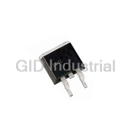
55V SINGLE N-CHNEL HEXFET POWER MOSFET TO-262 PKG
Part Number
IRF1010NLPBF
Price
Request Quote
Manufacturer
INTERNATIONAL RECTIFIER
Lead Time
Request Quote
Category
SEMICONDUCTORS
Datasheet

Extracted Text
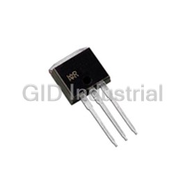
PD - 94171 IRF1010NS IRF1010NL � Advanced Process Technology ® HEXFET Power MOSFET � Ultra Low On-Resistance � Dynamic dv/dt Rating D V = 55V DSS � 175°C Operating Temperature � Fast Switching R = 11mΩ � Fully Avalanche Rated DS(on) G Description ® Advanced HEXFET Power MOSFETs from I = 85A� D International Rectifier utilize advanced processing S techniques to achieve extremely low on-resistance per silicon area. This benefit, combined with the fast switching speed and ruggedized device design that HEXFET power MOSFETs are well known for, provides the designer with an extremely efficient and reliable device for use in a wide variety of applications. 2 The D Pak is a surface mount power package capable of accommodating die sizes up to HEX-4. It provides the highest power capability and the lowest possible on- resistance in any existing surface mount package. The 2 2 D Pak TO-262 D Pak is suitable for high current applications because of its IRF1010NS IRF1010NL low internal connection resistance and can dissipate up to 2.0W in a typical surface mount application. The through-hole version (IRF1010NL) is available for low- profile applications. Absolute Maximum Ratings Parameter Max. Units I @ T = 25°C Continuous Drain Current, V @ 10V � 85� D C GS I @ T = 100°C Continuous Drain Current, V @ 10V � 60 A D C GS I Pulsed Drain Current �� 290 DM P @T = 25°C Power Dissipation 180 W D C Linear Derating Factor 1.2 W/°C V Gate-to-Source Voltage ± 20 V GS I Avalanche Current� 43 A AR E Repetitive Avalanche Energy� 18 mJ AR dv/dt Peak Diode Recovery dv/dt �� 3.6 V/ns T Operating Junction and -55 to + 175 J T Storage Temperature Range STG °C Soldering Temperature, for 10 seconds 300 (1.6mm from case ) Mounting torque, 6-32 or M3 srew 10 lbfin (1.1Nm) Thermal Resistance Parameter Typ. Max. Units R Junction-to-Case ––– 0.85 θJC R Junction-to-Ambient ( PCB Mounted,steady-state)** ––– 40 °C/W θJA www.irf.com 1 02/14/02 IRF1010NS/IRF1010NL Electrical Characteristics @ T = 25°C (unless otherwise specified) J Parameter Min. Typ. Max. Units Conditions V Drain-to-Source Breakdown Voltage 55 ––– ––– VV = 0V, I = 250µA (BR)DSS GS D ΔV /ΔT Breakdown Voltage Temp. Coefficient ––– 0.058 ––– V/°C Reference to 25°C, I = 1mA � (BR)DSS J D R Static Drain-to-Source On-Resistance ––– ––– 11 mΩ V = 10V, I = 43A�� DS(on) GS D V Gate Threshold Voltage 2.0 ––– 4.0 V V = V , I = 250µA GS(th) DS GS D g Forward Transconductance 32 ––– ––– SV = 25V, I = 43A�� fs DS D ––– ––– 25 V = 55V, V = 0V DS GS I Drain-to-Source Leakage Current µA DSS ––– ––– 250 V = 44V, V = 0V, T = 150°C DS GS J Gate-to-Source Forward Leakage ––– ––– 100 V = 20V GS I nA GSS Gate-to-Source Reverse Leakage ––– ––– -100 V = -20V GS Q Total Gate Charge ––– ––– 120 I = 43A g D Q Gate-to-Source Charge ––– ––– 19 nC V = 44V gs DS Q Gate-to-Drain ("Miller") Charge ––– ––– 41 V = 10V, See Fig. 6 and 13��� gd GS t Turn-On Delay Time ––– 13 ––– V = 28V d(on) DD t Rise Time ––– 76 ––– I = 43A r D ns t Turn-Off Delay Time ––– 39 ––– R = 3.6Ω d(off) G t Fall Time ––– 48 ––– V = 10V, See Fig. 10 �� f GS D Between lead, L Internal Drain Inductance ––– 4.5 ––– D 6mm (0.25in.) nH G from package L Internal Source Inductance ––– 7.5 ––– S and center of die contact S C Input Capacitance ––– 3210 ––– V = 0V iss GS C Output Capacitance ––– 690 ––– V = 25V oss DS C Reverse Transfer Capacitance ––– 140 ––– pF ƒ = 1.0MHz, See Fig. 5 � rss E Single Pulse Avalanche Energy�� ––– 1030�250� mJ I = 4.3A, L = 270µH AS AS Source-Drain Ratings and Characteristics Parameter Min. Typ. Max. Units Conditions D I Continuous Source Current MOSFET symbol S ––– ––– 85� (Body Diode) showing the A G I Pulsed Source Current integral reverse SM ––– ––– 290 S (Body Diode)� p-n junction diode. V Diode Forward Voltage ––– ––– 1.3 V T = 25°C, I = 43A, V = 0V � SD J S GS t Reverse Recovery Time ––– 69 100 ns T = 25°C, I = 43A rr J F Q Reverse Recovery Charge ––– 220 230 nC di/dt = 100A/µs �� rr t Forward Turn-On Time Intrinsic turn-on time is negligible (turn-on is dominated by L +L ) on S D Notes: � Repetitive rating; pulse width limited by � This is a calculated value limited to T = 175°C . J max. junction temperature. ( See fig. 11 ) � Calculated continuous current based on maximum allowable � Starting T = 25°C, L = 270µH J junction temperature. Package limitation current is 75A. R = 25Ω, I = 43A, V =10V (See Figure 12) G AS GS � Uses IRF1010N data and test conditions. � I ≤ 43A, di/dt ≤ 210A/µs, V ≤ V , SD DD (BR)DSS ** When mounted on 1" square PCB ( FR-4 or G-10 Material ). T ≤ 175°C J For recommended footprint and soldering techniques refer to � Pulse width ≤ 400µs; duty cycle ≤ 2%. application note #AN-994. � This is a typical value at device destruction and represents operation outside rated limits. 2 www.irf.com IRF1010NS/IRF1010NL 1000 1000 VGS VGS TOP 15V TOP 15V 10V 10V 8.0V 8.0V 7.0V 7.0V 6.0V 6.0V 5.5V 5.5V � � 5.0V 5.0V BOTTOM 4.5V BOTTOM 4.5V 100 100 4.5V 4.5V 10 10 20µs PULSE WIDTH 20µs PULSE WIDTH � ° � ° T = 175 C T = 25 C J J 1 1 0.1 1 10 100 0.1 1 10 100 V , Drain-to-Source Voltage (V) V , Drain-to-Source Voltage (V) DS DS Fig 1. Typical Output Characteristics Fig 2. Typical Output Characteristics 100 2.5 85A � I = D ° T = 25 C � J 2.0 ° � T = 175 C J 1.5 10 1.0 0.5 V = 25V DS � V = 10V � 20µs PULSE WIDTH GS 0.0 1 -60 -40 -20 0 20 40 60 80 100 120 140 160 180 4 6 8 10 12 ° T , Junction Temperature( C) V , Gate-to-Source Voltage (V) J GS Fig 3. Typical Transfer Characteristics Fig 4. Normalized On-Resistance Vs. Temperature www.irf.com 3 I , Drain-to-Source Current (A) I , Drain-to-Source Current (A) D D R , Drain-to-Source On Resistance DS(on) I , Drain-to-Source Current (A) (Normalized) D IRF1010NS/IRF1010NL 20 6000 I = 43A D � V = 0V, f = 1 MHZ GS C = C + C , C SHORTED iss gs gd ds V = 44V DS C = C 5000 V = 27V rss gd DS 16 � V = 11V C = C + C DS oss ds gd 4000 Ciss 12 3000 Coss 8 2000 4 1000 Crss FOR TEST CIRCUIT � SEE FIGURE 13 0 0 1 10 100 0 20 40 60 80 100 120 Q , Total Gate Charge (nC) G V , Drain-to-Source Voltage (V) DS Fig 6. Typical Gate Charge Vs. Fig 5. Typical Capacitance Vs. Gate-to-Source Voltage Drain-to-Source Voltage 1000 1000 OPERATION IN THIS AREA LIMITED BY R (on) DS 100 ° T = 175 C � J 100 100µsec 10 1msec 10 ° 1 T = 25 C � J Tc = 25°C Tj = 175°C 10msec V = 0 V Single Pulse � GS 1 0.1 0.0 0.6 1.2 1.8 2.4 1 10 100 1000 V ,Source-to-Drain Voltage (V) SD V , Drain-toSource Voltage (V) DS Fig 8. Maximum Safe Operating Area Fig 7. Typical Source-Drain Diode Forward Voltage 4 www.irf.com I , Reverse Drain Current (A) SD V , Gate-to-Source Voltage (V) GS C, Capacitance(pF) I , Drain-to-Source Current (A) D IRF1010NS/IRF1010NL 100 R D V � LIMITED BY PACKAGE DS V GS 80 D.U.T. R G + V - DD 60 V GS Pulse Width ≤ 1 µs Duty Factor ≤ 0.1 % 40 Fig 10a. Switching Time Test Circuit 20 V DS 90% 0 25 50 75 100 125 150 175 ° T , Case Temperature ( C) C 10% V GS Fig 9. Maximum Drain Current Vs. t t t t d(on) r d(off) f Case Temperature Fig 10b. Switching Time Waveforms 1 D = 0.50 0.20 0.10 0.1 0.05 P DM SINGLE PULSE 0.02 � t (THERMAL RESPONSE) 1 � 0.01 t 2 Notes: 1. Duty factor D = t / t 1 2 � 2. Peak T = P x Z + T J DM thJC C 0.01 0.00001 0.0001 0.001 0.01 0.1 t , Rectangular Pulse Duration (sec) 1 Fig 11. Maximum Effective Transient Thermal Impedance, Junction-to-Case www.irf.com 5 I , Drain Current (A) Thermal Response (Z ) D thJC IRF1010NS/IRF1010NL 500 15V I D TOP 18A 30A � 400 BOTTOM 43A L DRIVER V DS D.U.T R G + 300 V DD - I A AS 20V V GS t 0.01Ω p 200 Fig 12a. Unclamped Inductive Test Circuit 100 V (BR)DSS t p 0 25 50 75 100 125 150 175 ° Starting T , Junction Temperature( C) J Fig 12c. Maximum Avalanche Energy Vs. Drain Current I AS Fig 12b. Unclamped Inductive Waveforms Current Regulator Same Type as D.U.T. 50KΩ .2μF 12V .3μF Q G + V GS V DS D.U.T. - Q Q GS GD V GS V G 3mA I I G D Current Sampling Resistors Charge Fig 13b. Gate Charge Test Circuit Fig 13a. Basic Gate Charge Waveform 6 www.irf.com E , Single Pulse Avalanche Energy (mJ) AS IRF1010NS/IRF1010NL Peak Diode Recovery dv/dt Test Circuit + Circuit Layout Considerations D.U.T* • Low Stray Inductance • Ground Plane � • Low Leakage Inductance Current Transformer - + � � - + - � R G • dv/dt controlled by R + G • I controlled by Duty Factor "D" V SD DD - • D.U.T. - Device Under Test V GS * Reverse Polarity of D.U.T for P-Channel Driver Gate Drive P.W. Period D = Period P.W. V =10V [ ] *** GS D.U.T. I Waveform SD Reverse Recovery Body Diode Forward Current Current di/dt D.U.T. V Waveform DS Diode Recovery dv/dt V DD [ ] Re-Applied Voltage Body Diode Forward Drop Inductor Curent I [ ] SD Ripple ≤ 5% *** V = 5.0V for Logic Level and 3V Drive Devices GS ® Fig 14. For N-channel HEXFET power MOSFETs www.irf.com 7 IRF1010NS/IRF1010NL 2 D Pak Package Outline 10.54 (.415) - B - 10.16 (.400) 10.29 (.405) 4.69 (.185) REF. 4.20 (.165) 1.40 (.055) - A - 1.32 (.052) M AX. 1.22 (.048) 2 6.47 (.255) 6.18 (.243) 1.78 (.070) 15.49 (.610) 2.79 (.110) 1.27 (.050) 14.73 (.580) 2.29 (.090) 1 3 2.61 (.103) 5.28 (.208) 2.32 (.091) 4.78 (.188) 8.89 (.350) 1.40 (.055) 1.39 (.055) REF. 3X 1.14 (.045) 0.55 (.022) 1.14 (.045) 0.93 (.037) 3X 0.46 (.018) 0.69 (.027) 5.08 (.200) 0.25 (.010) M B A M MINIMUM RECOMMEND ED FOOTPRINT 11.43 (.450) LE AD ASSIGNM ENTS 8.89 (.350) NOTES: 1 - GATE 1 DIM ENS IONS AFTER SOLDER DIP. 17.78 (.700) 2 - DRAIN 2 DIM ENS IONIN G & TOLERANCING PER ANSI Y14.5M , 1982. 3 - SOURCE 3 CONTROLLIN G DIM ENSION : INCH. 4 HEATSINK & LEAD DIM ENSIONS DO NOT INCLUD E BURRS. 3.81 (.150) 2.54 (.100) 2.08 (.082) 2X 2X Part Marking Information 2 D Pak A INTERNATIONAL PART NUMBER RECTIFIER F530S LOGO 9246 DATE CODE 9B 1M (YYW W ) ASSEMBLY YY = YEAR LOT CODE WW = WEEK 8 www.irf.com IRF1010NS/IRF1010NL Package Outline TO-262 Outline Part Marking Information TO-262 www.irf.com 9 IRF1010NS/IRF1010NL Tape & Reel Information 2 D Pak TRR 1.60 (.063) 1.50 (.059) 1.60 (.063) 4.10 (.161) 1.50 (.059) 0.368 (.0145) 3.90 (.153) 0.342 (.0135) FEED DIRECTION 1.85 (.073) 11.60 (.457) 11.40 (.449) 1.65 (.065) 24.30 (.957) 15.42 (.609) 23.90 (.941) 15.22 (.601) TRL 1.75 (.069) 10.90 (.429) 1.25 (.049) 4.72 (.136) 10.70 (.421) 4.52 (.178) 16.10 (.634) 15.90 (.626) FEED DIRECTION 13.50 (.532) 27.40 (1.079) 12.80 (.504) 23.90 (.941) 4 330.00 60.00 (2.362) (14.173) M IN . MAX. 30.40 (1.197) NO TES : M AX. 1. C O M FO R M S TO EIA-418. 26.40 (1.039) 4 2. CO NTRO LLIN G DIM ENSIO N: M ILLIM ET ER. 24.40 (.961) 3. D IM ENSIO N M EASUR ED @ HU B. 3 4. INC LU D ES FLAN GE D ISTORT ION @ OU TER ED GE. Data and specifications subject to change without notice. This product has been designed and qualified for the Industrial market. Qualification Standards can be found on IR’s Web site. IR WORLD HEADQUARTERS: 233 Kansas St., El Segundo, California 90245, USA Tel: (310) 252-7105 TAC Fax: (310) 252-7903 Visit us at www.irf.com for sales contact information. 02/02 10 www.irf.com
Frequently asked questions
What makes Elite.Parts unique?

What kind of warranty will the IRF1010NLPBF have?
Which carriers does Elite.Parts work with?
Will Elite.Parts sell to me even though I live outside the USA?
I have a preferred payment method. Will Elite.Parts accept it?


What they say about us
FANTASTIC RESOURCE
One of our top priorities is maintaining our business with precision, and we are constantly looking for affiliates that can help us achieve our goal. With the aid of GID Industrial, our obsolete product management has never been more efficient. They have been a great resource to our company, and have quickly become a go-to supplier on our list!
Bucher Emhart Glass
EXCELLENT SERVICE
With our strict fundamentals and high expectations, we were surprised when we came across GID Industrial and their competitive pricing. When we approached them with our issue, they were incredibly confident in being able to provide us with a seamless solution at the best price for us. GID Industrial quickly understood our needs and provided us with excellent service, as well as fully tested product to ensure what we received would be the right fit for our company.
Fuji
HARD TO FIND A BETTER PROVIDER
Our company provides services to aid in the manufacture of technological products, such as semiconductors and flat panel displays, and often searching for distributors of obsolete product we require can waste time and money. Finding GID Industrial proved to be a great asset to our company, with cost effective solutions and superior knowledge on all of their materials, it’d be hard to find a better provider of obsolete or hard to find products.
Applied Materials
CONSISTENTLY DELIVERS QUALITY SOLUTIONS
Over the years, the equipment used in our company becomes discontinued, but they’re still of great use to us and our customers. Once these products are no longer available through the manufacturer, finding a reliable, quick supplier is a necessity, and luckily for us, GID Industrial has provided the most trustworthy, quality solutions to our obsolete component needs.
Nidec Vamco
TERRIFIC RESOURCE
This company has been a terrific help to us (I work for Trican Well Service) in sourcing the Micron Ram Memory we needed for our Siemens computers. Great service! And great pricing! I know when the product is shipping and when it will arrive, all the way through the ordering process.
Trican Well Service
GO TO SOURCE
When I can't find an obsolete part, I first call GID and they'll come up with my parts every time. Great customer service and follow up as well. Scott emails me from time to time to touch base and see if we're having trouble finding something.....which is often with our 25 yr old equipment.
ConAgra Foods