

 Manufacturers
INTEL RB80526PY850256

Description
Intel RB80526PY850256 Processor - 850 MHz, 100 MHz, 256 KB, 370 pin, SL4CC, Intel Pentium 3 Processor
Part Number
RB80526PY850256
Price
Request Quote
Manufacturer
INTEL
Lead Time
Request Quote
Category
PRODUCTS - R
Specifications
64 Bit Support
No
Brand
Intel
Clock Speed
850 MHz
Cooling Device
No
Core Stepping
cB0
Cores
Single Core
CPU ID String
0683h
CPU Socket Type
PGA370
Front Side Bus / QuickPath Interconnect
100 MHz
L2 Cache Size
256 KB
Manufacturing Technology
180 nm
Processor Code Name
Coppermine
Processor Type
Desktop
Series
Pentium III Processor
Thermal Power
22.5 Watts
Threads
1
Virtualization Technology Support
No
Voltage
1.65V
Datasheet

Extracted Text
® Pentium III Processor for the PGA370 Socket at 500 MHz to 1.13 GHz Datasheet Revision 8 Product Features Available in 1.13 GHz, 1B GHz, 933, 866,Dynamic execution micro architecture 800EB, 733, 667, 600EB, and 533EB MHz Intel Processor Serial Number for a 133 MHz system bus Power Management capabilities Available in 1.10 GHz, 1 GHz, 900, 850, —System Management mode 800, 750, 700, 650, 600E, 550E, and 500E MHz for a 100 MHz system bus —Multiple low-power states System bus frequency at 100 MHz andOptimized for 32-bit applications running on 133 MHz (“E” denotes support for advanced 32-bit operating systems Advanced Transfer Cache and Advanced Flip Chip Pin Grid Array (FC-PGA/FC-PGA2) system buffering; “B” denotes support for a packaging technology; FC-PGA/FC-PGA2 133 MHz system bus where both bus processors deliver high performance with frequencies are available for order per each improved handling protection and socketability given core frequency; See Table 1 for a Integrated high performance 16-KB instruction summary of features for each line item.) and 16-KB data, nonblocking, level one cache Available in versions that incorporate 256-KB Integrated Full Speed level two cache 256-KB Advanced Transfer Cache (on-die, allows for low latency on read/store operations full speed Level 2 (L2) cache with Error Correcting Code (ECC))Double Quad Word Wide (256 bit) cache data bus provides extremely high throughput on Dual Independent Bus (DIB) architecture: read/store operations. Separate dedicated external System Bus and dedicated internal high-speed cache bus8-way cache associativity provides improved cache hit rate on reads/store operations. Internet Streaming SIMD Extensions for enhanced video, sound and 3D performanceError-correcting code for System Bus data Binary compatible with applications runningEnables systems which are scaleable for up to on previous members of the Intel two processors microprocessor line ® The Pentium III processor is designed for high-performance desktops and for workstations and servers. It is binary compatible with previous Intel Architecture processors. The Pentium III processor provides great performance for applications running on advanced operating systems such as Windows* 98, Windows NT and UNIX*. This is achieved by integrating the best attributes of Intel processors— the dynamic execution, Dual Independent Bus architecture plus Intel MMX™ technology and Internet Streaming SIMD Extentions— bringing a new level of performance for systems buyers. The Pentium III processor is scaleable to two processors in a multiprocessor system and extends the power of the ® Pentium II processor with performance headroom for business media, communication and internet capabilities. Systems based on Pentium III processors also include the latest features to simplify system management and lower the cost of ownership for large and small business environments. The Pentium III processor offers great performance for today’s and tomorrow’s applications. FC-PGA370 Package June 2001 Document Number: 245264-08 ® Information in this document is provided in connection with Intel products. No license, express or implied, by estoppel or otherwise, to any intellectual property rights is granted by this document. Except as provided in Intel's Terms and Conditions of Sale for such products, Intel assumes no liability whatsoever, and Intel disclaims any express or implied warranty, relating to sale and/or use of Intel products including liability or warranties relating to fitness for a particular purpose, merchantability, or infringement of any patent, copyright or other intellectual property right. Intel products are not intended for use in medical, life saving, or life sustaining applications. Intel may make changes to specifications and product descriptions at any time, without notice. Designers must not rely on the absence or characteristics of any features or instructions marked "reserved" or "undefined." Intel reserves these for future definition and shall have no responsibility whatsoever for conflicts or incompatibilities arising from future changes to them. ® The Pentium III processor may contain design defects or errors known as errata which may cause the product to deviate from published specifcations. Current characterized errata are available on request. Contact your local Intel sales office or your distributor to obtain the latest specifications and before placing your product order. Copies of documents which have an ordering number and are referenced in this document, or other Intel literature may be obtained by calling 1-800-548-4725 or by visiting Intel's website at http://www.intel.com. Intel, Pentium II, Pentium III, Pentium Pro, Celeron and Intel387 are trademarks or registered trademarks of Intel Corporation or its subsidiaries inthe United States and other countries. *Other names and brands may be claimed as the property of others. Copyright © Intel Corporation, 2001 Datasheet ® Pentium III Processor for the PGA370 Socket at 500 MHz to 1.13 GHz Contents 1.0 Introduction ..................................................................................................................8 1.1 Terminology...........................................................................................................9 1.1.1 Package and Processor Terminology ......................................................9 1.1.2 Processor Naming Convention...............................................................10 1.2 Related Documents.............................................................................................11 2.0 Electrical Specifications........................................................................................13 2.1 Processor System Bus and V ........................................................................13 REF 2.2 Clock Control and Low Power States..................................................................14 2.2.1 Normal State—State 1 ...........................................................................15 2.2.2 AutoHALT Powerdown State—State 2...................................................15 2.2.3 Stop-Grant State—State 3 .....................................................................16 2.2.4 HALT/Grant Snoop State—State 4 ........................................................16 2.2.5 Sleep State—State 5..............................................................................16 2.2.6 Deep Sleep State—State 6 ....................................................................17 2.2.7 Clock Control..........................................................................................17 2.3 Power and Ground Pins ......................................................................................17 2.3.1 Phase Lock Loop (PLL) Power...............................................................18 2.4 Decoupling Guidelines .......................................................................................19 2.4.1 Processor VCC and AGTL+ (AGTL) Decoupling ...........................19 CORE 2.5 Processor System Bus Clock and Processor Clocking .......................................19 2.5.1 Mixing Processors of Different Frequencies...........................................20 2.6 Voltage Identification...........................................................................................20 2.7 Processor System Bus Unused Pins...................................................................22 2.8 Processor System Bus Signal Groups ................................................................22 2.8.1 Asynchronous vs. Synchronous for System Bus Signals.......................24 2.8.2 System Bus Frequency Select Signals (BSEL[1:0])...............................25 2.9 Maximum Ratings................................................................................................26 2.10 Processor DC Specifications...............................................................................27 2.10.1 ICC Slew Rate Specifications.................................................................33 2.11 AGTL / AGTL+ System Bus Specifications .........................................................36 2.12 System Bus AC Specifications ............................................................................37 2.12.1 I/O Buffer Model .....................................................................................37 3.0 Signal Quality Specifications ..............................................................................46 3.1 BCLK/BCLK# and PICCLK Signal Quality Specifications and Measurement Guidelines ...........................................................................................................46 3.2 AGTL+ / AGTL Signal Quality Specifications and Measurement Guidelines ......47 3.3 AGTL+ Signal Quality Specifications and Measurement Guidelines ..................48 3.3.1 Overshoot/Undershoot Guidelines .........................................................48 3.3.2 Overshoot/Undershoot Magnitude .........................................................49 3.3.3 Overshoot/Undershoot Pulse Duration...................................................49 3.3.4 Activity Factor.........................................................................................49 3.3.5 Reading Overshoot/Undershoot Specification Tables............................50 3.3.6 Determining if a System Meets the Overshoot/Undershoot Specifications .........................................................................................51 3.4 Non-AGTL+ (Non-AGTL) Signal Quality Specifications and Measurement Datasheet 3 ® Pentium III Processor for the PGA370 Socket at 500 MHz to 1.13 GHz Guidelines ...........................................................................................................54 3.4.1 Overshoot/Undershoot Guidelines .........................................................54 3.4.2 Ringback Specification...........................................................................55 3.4.3 Settling Limit Guideline ..........................................................................55 4.0 Thermal Specifications and Design Considerations.................................56 4.1 Thermal Specifications........................................................................................56 4.2 Processor Die Area .............................................................................................57 4.3 Thermal Diode.....................................................................................................58 5.0 Mechanical Specifications ..................................................................................60 5.1 FC-PGA Mechanical Specifications ....................................................................60 5.1.1 FC-PGA2 Mechanical Specifications .....................................................63 5.2 Processor Markings ............................................................................................65 5.2.1 Processor Markings for FC-PGA2..........................................................65 5.3 Recommended Mechanical Keep-Out Zones .....................................................66 5.4 Processor Signal Listing......................................................................................67 6.0 Boxed Processor Specifications .......................................................................80 ® ® 6.1 Mechanical Specifications for the Boxed Intel Pentium III Processor..............80 6.1.1 Boxed Processor Thermal Cooling Solution Dimensions.......................80 6.1.2 Boxed Processor Heatsink Weight.........................................................82 6.1.3 Boxed Processor Thermal Cooling Solution Clip ...................................82 6.2 Thermal Specifications........................................................................................82 6.2.1 Boxed Processor Cooling Requirements ...............................................82 ® ® 6.3 Electrical Requirements for the Boxed Intel Pentium III Processor.................83 6.3.1 Fan Heatsink Power Supply...................................................................83 7.0 Processor Signal Description.............................................................................85 7.1 Alphabetical Signals Reference ..........................................................................85 7.2 Signal Summaries...............................................................................................92 4 Datasheet ® Pentium III Processor for the PGA370 Socket at 500 MHz to 1.13 GHz Figures 1 Second Level (L2) Cache Implementation ...........................................................8 2 AGTL+/AGTL Bus Topology in a Uniprocessor Configuration ............................14 3 AGTL+/AGTL Bus Topology in a Dual-Processor Configuration ........................14 4 Stop Clock State Machine...................................................................................15 5 Processor Vcc Package Routing ................................................................18 CMOS 6 Differential Clocking Example .............................................................................20 7 BSEL[1:0] Example for a 100/133 MHz or 100 MHz Only System Design .........25 8 Slew Rate (23A Load Step).................................................................................33 9 Generic Clock Waveform ....................................................................................41 10 BCLK, PICCLK, and TCK Generic Clock Waveform...........................................42 11 System Bus Valid Delay Timings ........................................................................42 12 System Bus Setup and Hold Timings..................................................................43 13 System Bus Reset and Configuration Timings....................................................43 14 Platform Power-On Sequence Timings...............................................................44 15 Power-On Reset and Configuration Timings.......................................................45 16 BCLK, PICCLK Generic Clock Waveform at the Processor Pins........................47 17 Low to High AGTL+ Receiver Ringback Tolerance.............................................48 18 Maximum Acceptable AGTL+ Overshoot/Undershoot Waveform.......................53 19 Maximum Acceptable AGTL Overshoot/Undershoot Waveform .........................53 20 Non-AGTL+ (Non-AGTL) Overshoot/Undershoot, Settling Limit, and Ringback 1 ..........................................................................................................54 21 Processor Functional Die Layout for FC-PGA.....................................................58 22 FC-PGA and FC-PGA2 Package Types .............................................................60 23 Package Dimensions...........................................................................................61 24 Package Dimensions for FC-PGA2.....................................................................63 25 FC-PGA2 Flatness Specification.........................................................................64 26 Top Side Processor Markings for FC-PGA (up to CPUID 0x686H) ....................65 27 Top Side Processor Markings for FC-PGA (for CPUID 0x68AH)).......................65 28 Top Side Processor Markings for FC-PGA2 .......................................................66 29 Volumetric Keep-Out for FC-PGA and FC-PGA2................................................66 30 Component Keep-Out .........................................................................................67 ® ® 31 Intel Pentium III Processor Pinout ...................................................................68 ® ® 32 Conceptual Boxed Intel Pentium III Processor for the PGA370 Socket ..........80 33 Dimensions of Mechanical Step Feature in Heatsink Base.................................81 34 Dimensions of Notches in Heatsink Base ...........................................................82 ® ® 35 Thermal Airspace Requirement for all Boxed Intel Pentium III Processor Fan Heatsinks in the PGA370 Socket ........................................................................83 36 Boxed Processor Fan Heatsink Power Cable Connector Description.................84 37 Motherboard Power Header Placement Relative to the Boxed ® ® Intel Pentium III Processor ..............................................................................84 Datasheet 5 ® Pentium III Processor for the PGA370 Socket at 500 MHz to 1.13 GHz Tables 1 Processor Identification.......................................................................................10 2 Voltage Identification Definition...........................................................................21 3 System Bus Signal Groups 1 ..............................................................................23 4 System Bus Signal Groups (AGTL)1 ..................................................................23 5 Frequency Select Truth Table for BSEL[1:0] ......................................................26 6 Absolute Maximum Ratings ................................................................................26 7 Voltage and Current Specifications ....................................................................28 8 PL Slew Rate Data (23A) ....................................................................................33 9 AGTL / AGTL+ Signal Groups DC Specifications ..............................................34 10 Non-AGTL+ Signal Group DC Specifications .....................................................34 11 Non-AGTL Signal Group DC Specifications .......................................................35 12 Processor AGTL+ Bus Specifications ................................................................36 13 Processor AGTL Bus Specifications ..................................................................36 14 System Bus AC Specifications (SET Clock) .......................................................37 15 System Bus Timing Specifications (Differential Clock) .......................................38 16 System Bus AC Specifications (AGTL+ or AGTL Signal Group) ........................39 17 System Bus AC Specifications (CMOS Signal Group) .......................................40 18 System Bus AC Specifications (Reset Conditions) ............................................40 19 System Bus AC Specifications (APIC Clock and APIC I/O)................................40 20 Platform Power-On Timings ................................................................................40 21 BCLK/PICCLK Signal Quality Specifications for Simulation at the Processor Pins ...................................................................................................46 22 BCLK/PICCLK Signal Quality Specifications for Simulation at the Processor Pins in a Differential Clock Platform for AGTL ............................................................46 23 AGTL+ Signal Groups Ringback Tolerance Specifications at the Processor Pins ....................................................................................................................47 24 Example Platform Information.............................................................................50 25 100 MHz AGTL+ / AGTL Signal Group Overshoot/Undershoot Tolerance at Processor Pins....................................................................................................51 26 133 MHz AGTL+/AGTL Signal Group Overshoot/Undershoot Tolerance ..........52 27 33 MHz CMOS Signal Group Overshoot/Undershoot Tolerance at Processor Pins....................................................................................................52 28 Signal Ringback Specifications for Non-AGTL+ Signal Simulations at the Processor Pins....................................................................................................55 29 Signal Ringback Specifications for Non-AGTL Signal Simulations at the Processor Pins .............................................................................................55 30 Intel® Pentium® III Processor Thermal Design Power for the FC-PGA Package .. 56 31 Intel® Pentium® III Processor for the FC-PGA2 Package Thermal Design Power......................................................................................................57 32 Processor Functional Die Layout for FC-PGA ....................................................58 33 Thermal Diode Parameters.................................................................................59 34 Thermal Diode Interface......................................................................................59 35 Intel® Pentium® III Processor Package Dimensions..........................................61 36 Processor Die Loading Parameters for FC-PGA ................................................62 37 Package Dimensions for Intel® Pentium® III Processor FC-PGA2 Package .....63 38 Processor Case Loading Parameters for FC-PGA2 ...........................................64 39 Signal Listing in Order by Signal Name ..............................................................69 40 Signal Listing in Order by Pin Number ................................................................74 6 Datasheet ® Pentium III Processor for the PGA370 Socket at 500 MHz to 1.13 GHz 41 Fan Heatsink Power and Signal Specifications...................................................84 42 Signal Description ...............................................................................................85 43 Output Signals.....................................................................................................92 44 Input Signals........................................................................................................92 45 Input/Output Signals (Single Driver)....................................................................94 46 Input/Output Signals (Multiple Driver) .................................................................94 Datasheet 7 ® Pentium III Processor for the PGA370 Socket at 500 MHz to 1.13 GHz 1.0 Introduction ® ® The Intel Pentium III processor for the PGA370 socket is the next member of the P6 family, in the Intel IA-32 processor line and hereafter will be referred to as the “Pentium III processor”, or simply “the processor”. The processor uses the same core and offers the same performance as the Pentium III processor for the SC242 connector, but utilizes a package technology called flip-chip pin grid array, or FC-PGA. This package utilizes the same 370-pin zero insertion force socket ® TM (PGA370) used by the Intel Celeron processor. Thermal solutions are attached directly to the back of the processor core package without the use of a thermal plate or heat spreader. As core frequencies increase, the need for better power dissipation arises, so an Integrated Heat Spreader (IHS) has been introduced at the higher frequencies near 1B GHz. The package with an IHS is called FC-PGA2. The Pentium III processor, like its predecessors in the P6 family of processors, implements a Dynamic Execution microarchitecture—a unique combination of multiple branch prediction, data flow analysis, and speculative execution. This enables these processors to deliver higher performance than the Pentium processor, while maintaining binary compatibility with all previous ® TM Intel Architecture processors. The processor also executes Intel MMX technology instructions for enhanced media and communication performance just as it’s predecessor, the Pentium III processor. Additionally, Pentium III processor executes Streaming SIMD (single-instruction, multiple data) Extensions for enhanced floating point and 3-D application performance. The concept of processor identification, via CPUID, is extended in the processor family with the ® addition of a processor serial number. Refer to the Intel Processor Serial Number application note for more detailed information. The processor utilizes multiple low-power states such as AutoHALT, Stop-Grant, Sleep, and Deep Sleep to conserve power during idle times. The processor includes an integrated on-die, 256-KB, 8-way set associative level-two (L2) cache. The L2 cache implements the new Advanced Transfer Cache Architecture with a 256-bit wide bus. The processor also includes a 16-KB level one (L1) instruction cache and 16-KB L1 data cache. These cache arrays run at the full speed of the processor core. As with the Pentium III processor for the SC242 connector, the Pentium III processor for the PGA370 socket has a dedicated L2 cache bus, thus maintaining the dual independent bus architecture to deliver high bus bandwidth and performance (see Figure 1). Memory is cacheable for 64 GB of addressable memory space, allowing significant headroom for desktop systems. Refer to the Specification Update document for this processor to determine the cacheability and cache configuration options for a specific processor. The Specification Update document can be requested at your nearest Intel sales office. The processor utilizes the same multiprocessing system bus technology as the Pentium II processor. This allows for a higher level of performance for both uni-processor and two-way multiprocessor systems. The system bus uses a variant of GTL+ signaling technology called Assisted Gunning Transceiver Logic (AGTL+/AGTL) signaling technology. Figure 1. Second Level (L2) Cache Implementation L2 Processor Processor Tag L2 Core Core ® ® ® ® Intel Pentium III SECC2 Processor Intel Pentium III FC-PGA Processor 8 Datasheet ® Pentium III Processor for the PGA370 Socket at 500 MHz to 1.13 GHz 1.1 Terminology In this document, a ‘#’ symbol after a signal name refers to an active low signal. This means that a signal is in the active state (based on the name of the signal) when driven to a low level. For example, when FLUSH# is low, a flush has been requested. When NMI is high, a nonmaskable interrupt has occurred. In the case of signals where the name does not imply an active state but describes part of a binary sequence (such as address or data), the ‘#’ symbol implies that the signal is inverted. For example, D[3:0] = ‘HLHL’ refers to a hex ‘A’, and D[3:0]# = ‘LHLH’ also refers to a hex ‘A’ (H= High logic level, L= Low logic level). The term “system bus” refers to the interface between the processor, system core logic (a.k.a. the chipset components), and other bus agents. 1.1.1 Package and Processor Terminology The following terms are used often in this document and are explained here for clarification: Pentium III processor - The entire product including all internal components. PGA370 socket - 370-pin Zero Insertion Force (ZIF) socket which a FC-PGA or PPGA packaged processor plugs into. FC-PGA - Flip Chip Pin Grid Array. The package technology used on Pentium III processors for the PGA370 socket. FC-PGA2 - Flip Chip Pin Grid Array with an Integrated Heat Spreader (IHS). The package technology used on Pentium III processors for the PGA370 socket for increased power dissipation away from the die. The IHS covers the die and has a very low thermal resistance. Integrated Heat Spreader (IHS) - The IHS is a metal cover on the die and is an integral part of the CPU. The IHS promotes heat spreading away from the die backside to ease thermal constraints. Advanced Transfer Cache (ATC) - New L2 cache architecture unique to the 0.18 micron Pentium III processors. ATC consists of microarchitectural improvements that provide a higher data bandwidth interface into the processor core that is completely scaleable with the processor core frequency. Keep-out zone - The area on or near a FC-PGA packaged processor that system designs can not utilize. Keep-in zone - The area of a FC-PGA packaged processor that thermal solutions may utilize. OLGA - Organic Land Grid Array. The package technology for the core used in S.E.C.C. 2 processors that permits attachment of the heatsink directly to the die. PPGA - Plastic Pin Grid Array. The package technology used for Celeron processors that utilize the PGA370 socket. Processor - For this document, the term processor is the generic form of the Pentium III processor for the PGA370 socket in the FC-PGA package. Processor core - The processor’s execution engine. S.E.C.C. - The processor package technology called “Single Edge Contact Cartridge”. Used ® ® with Intel Pentium II processors. S.E.C.C. 2 - The follow-on to S.E.C.C. processor package technology. This differs from its predecessor in that it has no extended thermal plate, thus reducing thermal resistance. Used with Pentium III processors and latest versions of the Pentium II processor. Datasheet 9 ® Pentium III Processor for the PGA370 Socket at 500 MHz to 1.13 GHz SC242 - The 242-contact slot connector (previously referred to as slot 1 connector) that the ® ® S.E.C.C. and S.E.C.C. 2 plug into, just as the Intel Pentium Pro processor uses socket 8. The cache and L2 cache are an industry designated names. 1.1.2 Processor Naming Convention A letter(s) is added to certain processors (e.g., 600EB MHz) when the core frequency alone may not uniquely identify the processor. Below is a summary of what each letter means as well as a table listing all the available Pentium III processors for the PGA370 socket. “B” — 133 MHz System Bus Frequency “E” — Processor with “Advanced Transfer Cache” (CPUID 068xh and greater) Table 1. Processor Identification System Bus Core Frequency L2 Cache Size L2 Cache 1 Processor Frequency CPUID 2 (MHz) (Kbytes) Type (MHz) 500E 500 100 256 ATC 068xh 533EB 533 133 256 ATC 068xh 550E 550 100 256 ATC 068xh 600E 600 100 256 ATC 068xh 600EB 600 133 256 ATC 068xh 650 650 100 256 ATC 068xh 667 667 133 256 ATC 068xh 700 700 100 256 ATC 068xh 733 733 133 256 ATC 068xh 750 750 100 256 ATC 068xh 800 800 100 256 ATC 068xh 800EB 800 133 256 ATC 068xh 850 850 100 256 ATC 068xh 866 866 133 256 ATC 068xh 900 900 100 256 ATC 068xh 933 933 133 256 ATC 068xh 1 GHz 1000 100 256 ATC 068xh 1B GHz 1000 133 256 ATC 068xh 1.10 GHz 1100 100 256 ATC 068xh 1.13 GHz 1133 133 256 ATC 068xh NOTES: ® 1. Refer to the Pentium III Processor Specification Update for the exact CPUID for each processor. 2. ATC = Advanced Transfer Cache. ATC is an L2 Cache integrated on the same die as the processor core. With ATC, the interface between the processor core and L2 Cache is 256-bits wide, runs at the same frequency as the processor core and has enhanced buffering. 10 Datasheet ® Pentium III Processor for the PGA370 Socket at 500 MHz to 1.13 GHz 1.2 Related Documents The reader of this specification should also be familiar with material and concepts presented in the 1,2 following documents : Document Intel Document Number ® AP-485, Intel Processor Identification and the CPUID Instruction 241618 ® AP-585, Pentium II Processor GTL+ Guidelines 243330 AP-589, Design for EMI 243334 ® AP-905, Pentium III Processor Thermal Design Guidelines 245087 ® AP-907, Pentium III Processor Power Distribution Guidelines 245085 ® AP-909, Intel Processor Serial Number 245125 ® Intel Architecture Software Developer's Manual 243193 Volume I: Basic Architecture 243190 Volume II: Instruction Set Reference 243191 Volume III: System Programming Guide 243192 P6 Family of Processors Hardware Developer’s Manual 244001 ® Pentium II Processor Developer’s Manual 243502 ® Pentium III Processor Datasheet for SECC2 244452 ® Pentium III Processor Datasheet for PGA370 245264 ® Pentium III Processor Specification Update 244453 ® TM Intel Celeron Processor Datasheet 243658 ® TM Intel Celeron Processor Specification Update 243748 370-Pin Socket (PGA370) Design Guidelines 244410 PGA370 Heat Sink Cooling in MicroATX Chassis 245025 ® Intel 810E Chipset Platform Design Guide 290675 ® 3 Intel 815 B-step Chipset Platform Design Guide ® Intel 815E Chipset Platform Design Guide 298234 ® Intel 820 Chipset Platform Design Guide 290631 ® Intel 840 Chipset Platform Design Guide 298021 CK98 Clock Synthesizer/Driver Design Guidelines 245338 ® 3 Intel 810E Chipset Clock Synthesizer/Driver Specification VRM 8.4 DC-DC Converter Design Guidelines 245335 Pentium III Processor for the PGA370 Socket I/O Buffer Models, XTK/XNS* 3 Format ® 3 Pentium Pro Processor BIOS Writer’s Guide ® 3 Extensions to the Pentium Pro Processor BIOS Writer’s Guide rev. 3.7 ® Pentium III Thermal/Mechanical Solution Functional Guidelines 245241 ® ® Intel Pentium III Processor in the FC-PGA2 Package Thermal Design Guide 249660 Datasheet 11 ® Pentium III Processor for the PGA370 Socket at 500 MHz to 1.13 GHz NOTES: 1. Unless otherwise noted, this reference material can be found on the Intel Developer’s Website located at http://developer.intel.com. 2. For a complete listing of Pentium III processor reference material, please refer to the Intel Developer’s Website at http://developer.intel.com/design/PentiumIII/. 3. This material is available through an Intel field sales representative. 12 Datasheet ® Pentium III Processor for the PGA370 Socket at 500 MHz to 1.13 GHz 2.0 Electrical Specifications 2.1 Processor System Bus and V REF The Pentium III processor signals use a variation of the low voltage Gunning Transceiver Logic (GTL) signaling technology. The Pentium Pro processor system bus specification is similar to the GTL specification, but was enhanced to provide larger noise margins and reduced ringing. The improvements are accomplished by increasing the termination voltage level and controlling the edge rates. This specification is different from the GTL specification, and is referred to as GTL+. For more ® ® information on GTL+ specifications, see the GTL+ buffer specification in the Intel Pentium II Processor Developer’s Manual. Current P6 family processors vary from the Pentium Pro processor in their output buffer implementation. The buffers that drive the system bus signals on the Celeron, Pentium II, and Pentium III processors are actively driven to V for one clock cycle after the low to high transition TT to improve rise times. These signals should still be considered open-drain and require termination to a supply that provides the high signal level. Because this specification is different from the standard GTL+ specification, it is referred to as AGTL+, or Assisted GTL+ in this and other documentation. AGTL+ logic and GTL+ logic are compatible with each other and may both be used on the same system bus. For more information on AGTL+ routing, see the appropriate platform design guide. Note that some Pentium III processors with CPUID 068xh support the AGTL specification in addition to the AGTL+ specification. AGTL logic and AGTL+ logic are not compatible with each other due to differences with the signal switching levels. Processors that do not support the AGTL specification cannot be installed into platforms where the chipset only supports the AGTL signal levels. For more information on AGTL or AGTL+ routing, please refer to the appropriate platform design guide. Both AGTL and AGTL+ inputs use differential receivers which require a reference signal (V ). REF V is used by the receivers to determine if a signal is a logical 0 or a logical 1, and is supplied by REF the motherboard to the PGA370 socket for the processor core. Local V copies should also be REF generated on the motherboard for all other devices on the AGTL+ (AGTL) system bus. Termination (usually a resistor at each end of the signal trace) is used to pull the bus up to the high voltage level and to control reflections on the transmission line. The processor contains on-die termination resistors that provide termination for one end of the bus, except for RESET#. These specifications assume another resistor at the end of each signal trace to ensure adequate signal quality for the AGTL+ (AGTL) signals and provide backwards compatibility for the Celeron processor; see Table ® ® 12 for the bus termination voltage specifications for AGTL+. Refer to the Intel Pentium II Processor Developer’s Manual for the AGTL+ bus specification. Solutions exist for single-ended termination as well, though this implementation changes system design and eliminate backwards compatibility for Celeron processors in the PPGA package. Single-ended termination designs must still provide an AGTL+ (AGTL) termination resistor on the motherboard for the RESET# signal. Figure 2 is a schematic representation of the AGTL+ (AGTL) bus topology for the Pentium III processors in the PGA370 socket. Figure 3 is a schematic representation of the AGTL+/AGTL bus topology in a dual-processor configuration with Pentium III processors in the PGA370 socket. Both AGTL+ and AGTL bus depend on incident wave switching. Therefore, timing calculations for AGTL+ or AGTL signals are based on flight time as opposed to capacitive deratings. Analog signal simulation of the system bus including trace lengths is highly recommended when designing a Datasheet 13 ® Pentium III Processor for the PGA370 Socket at 500 MHz to 1.13 GHz system with a heavily loaded AGTL+ bus, especially for systems using a single set of termination resistors (i.e., those on the processor die). Such designs will not match the solution space allowed for by installation of termination resistors on the baseboard. Figure 2. AGTL+/AGTL Bus Topology in a Uniprocessor Configuration Processor Chipset Figure 3. AGTL+/AGTL Bus Topology in a Dual-Processor Configuration Processor Chipset Processor 2.2 Clock Control and Low Power States Processors allow the use of AutoHALT, Stop-Grant, Sleep, and Deep Sleep states to reduce power consumption by stopping the clock to internal sections of the processor, depending on each particular state. See Figure 4 for a visual representation of the processor low-power states. 14 Datasheet ® Pentium III Processor for the PGA370 Socket at 500 MHz to 1.13 GHz Figure 4. Stop Clock State Machine HALT Instruction and HALT Bus Cycle Generated 1. Normal State 2. Auto HALT Power Down State INIT#, BINIT#, INTR, Normal execution. BCLK running. , NMI SMI#, RESET# Snoops and interrupts allowed. STPCLK# Asserted STPCLK# De-asserted STPCLK# STPCLK# Snoop Snoop and Stop-Grant State Asserted De-asserted Event Event entered from Occurs Serviced AutoHALT Snoop Event Occurs 3. Stop Grant State 4. HALT/Grant Snoop State BCLK running. BCLK running. Snoop Event Serviced Snoops and interrupts allowed. Service snoops to caches. SLP# SLP# Asserted De-asserted 5. Sleep State BCLK running. No snoops or interrupts allowed. BCLK BCLK Input Input Stopped Restarted 6. Deep Sleep State BCLK stopped. No snoops or interrupts allowed. PCB757a For the processor to fully realize the low current consumption of the Stop-Grant, Sleep and Deep Sleep states, a Model Specific Register (MSR) bit must be set. For the MSR at 02AH (Hex), bit 26 must be set to a ‘1’ (this is the power on default setting) for the processor to stop all internal clocks during these modes. For more information, see the Intel Architecture Software Developer’s Manual, Volume 3: System Programming Guide located on the developer.intel.com website. 2.2.1 Normal State—State 1 This is the normal operating state for the processor. 2.2.2 AutoHALT Powerdown State—State 2 AutoHALT is a low power state entered when the processor executes the HALT instruction. The processor transitions to the Normal state upon the occurrence of SMI#, INIT#, or LINT[1:0] (NMI, INTR). RESET# causes the processor to immediately initialize itself. The return from a System Management Interrupt (SMI) handler can be to either Normal Mode or the AutoHALT Power Down state. See the Intel Architecture Software Developer's Manual, Volume III: System Programmer's Guide for more information. FLUSH# is serviced during the AutoHALT state, and the processor will return to the AutoHALT state. Datasheet 15 ® Pentium III Processor for the PGA370 Socket at 500 MHz to 1.13 GHz The system can generate a STPCLK# while the processor is in the AutoHALT Power Down state. When the system deasserts the STPCLK# interrupt, the processor returns execution to the HALT state. 2.2.3 Stop-Grant State—State 3 The Stop-Grant state on the processor is entered when the STPCLK# signal is asserted. Since the AGTL+ signal pins receive power from the system bus, these pins should not be driven (allowing the level to return to VTT) for minimum power drawn by the termination resistors in this state. In addition, all other input pins on the system bus should be driven to the inactive state. BINIT# and FLUSH# are not serviced during the Stop-Grant state. RESET# causes the processor to immediately initialize itself, but the processor stays in Stop-Grant state. A transition back to the Normal state occurs with the deassertion of the STPCLK# signal. A transition to the HALT/Grant Snoop state occurs when the processor detects a snoop on the system bus (see Section 2.2.4). A transition to the Sleep state (see Section 2.2.5) occurs with the assertion of the SLP# signal. While in Stop-Grant State, SMI#, INIT#, and LINT[1:0] are latched by the processor, and only serviced when the processor returns to the Normal state. Only one occurrence of each event is recognized and serviced upon return to the Normal state. 2.2.4 HALT/Grant Snoop State—State 4 The processor responds to snoop transactions on the system bus while in Stop-Grant state or in AutoHALT Power Down state. During a snoop transaction, the processor enters the HALT/Grant Snoop state. The processor stays in this state until the snoop on the system bus has been serviced (whether by the processor or another agent on the system bus). After the snoop is serviced, the processor returns to the Stop-Grant state or AutoHALT Power Down state, as appropriate. 2.2.5 Sleep State—State 5 The Sleep state is a very low power state in which the processor maintains its context, maintains the phase-locked loop (PLL), and has stopped all internal clocks. The Sleep state can only be entered from the Stop-Grant state. Once in the Stop-Grant state, the SLP# pin can be asserted, causing the processor to enter the Sleep state. The SLP# pin is not recognized in the Normal or AutoHALT states. Snoop events that occur while in Sleep state or during a transition into or out of Sleep state will cause unpredictable behavior. In the Sleep state, the processor is incapable of responding to snoop transactions or latching interrupt signals. No transitions or assertions of signals (with the exception of SLP# or RESET#) are allowed on the system bus while the processor is in Sleep state. Any transition on an input signal before the processor has returned to Stop-Grant state will result in unpredictable behavior. If RESET# is driven active while the processor is in the Sleep state, and held active as specified in the RESET# pin specification, then the processor will reset itself, ignoring the transition through Stop-Grant State. If RESET# is driven active while the processor is in the Sleep State, the SLP# and STPCLK# signals should be deasserted immediately after RESET# is asserted to ensure the processor correctly executes the reset sequence. 16 Datasheet ® Pentium III Processor for the PGA370 Socket at 500 MHz to 1.13 GHz While in the Sleep state, the processor is capable of entering its lowest power state, the Deep Sleep state, by stopping the BCLK input (see Section 2.2.6). Once in the Sleep or Deep Sleep states, the SLP# pin can be deasserted if another asynchronous system bus event occurs. The SLP# pin has a minimum assertion of one BCLK period. 2.2.6 Deep Sleep State—State 6 The Deep Sleep state is the lowest power state the processor can enter while maintaining context. 1 The Deep Sleep state is entered by stopping the BCLK input (after the Sleep state was entered from the assertion of the SLP# pin). The processor is in Deep Sleep state immediately after BCLK 1 is stopped. It is recommended that the BCLK input be held low during the Deep Sleep State. 1 Stopping of the BCLK input lowers the overall current consumption to leakage levels. To re-enter the Sleep state, the BCLK input must be restarted. A period of 1 ms (to allow for PLL stabilization) must occur before the processor can be considered to be in the Sleep state. Once in the Sleep state, the SLP# pin can be deasserted to re-enter the Stop-Grant state. While in Deep Sleep state, the processor is incapable of responding to snoop transactions or latching interrupt signals. No transitions or assertions of signals are allowed on the system bus while the processor is in Deep Sleep state. Any transition on an input signal before the processor has returned to Stop-Grant state will result in unpredictable behavior. 2.2.7 Clock Control 2 BCLK provides the clock signal for the processor and on die L2 cache. During AutoHALT Power Down and Stop-Grant states, the processor will process a system bus snoop. The processor does not stop the clock to the L2 cache during AutoHALT Power Down or Stop-Grant states. Entrance into the Halt/Grant Snoop state allows the L2 cache to be snooped, similar to the Normal state. When the processor is in Sleep and Deep Sleep states, it does not respond to interrupts or snoop transactions. During the Sleep state, the internal clock to the L2 cache is not stopped. During the Deep Sleep state, the internal clock to the L2 cache is stopped. The internal clock to the L2 cache is restarted only after the internal clocking mechanism for the processor is stable (i.e., the processor has re-entered Sleep state). PICCLK should not be removed during the AutoHALT Power Down or Stop-Grant states. PICCLK can be removed during the Sleep or Deep Sleep states. When transitioning from the Deep 2 Sleep state to the Sleep state, PICCLK must be restarted with BCLK. 2.3 Power and Ground Pins The operating voltage of the Pentium III processor for the PGA370 socket is the same for the core and the L2 cache; VCC . There are four pins defined on the package for voltage identification CORE (VID). These pins specify the voltage required by the processor core. These have been added to cleanly support voltage specification variations on current and future processors. For clean on-chip power and voltage reference distribution, the Pentium III processors in the PGA370 socket have 75 VCC ,8V (7 for AGTL platforms), 15 VTT, and 77 VSS (ground) CORE REF inputs. VCC inputs supply the processor core, including the on-die L2 cache. VTT inputs CORE 1. For processors using AGTL level bus with differential clocking, the deep sleep state is entered by stopping BCLK and BCLK# input. 2. For processors using AGTL level bus with differential clocking this would also include the BCLK# signal as well. Datasheet 17 ® Pentium III Processor for the PGA370 Socket at 500 MHz to 1.13 GHz (1.5 V/1.25 V) are used to provide an AGTL+/AGTL termination voltage to the processor, and the V inputs are used as the AGTL+/AGTL reference voltage for the processor. Note that not all REF VTT inputs must be connected to the VTT supply. Refer to Section 5.4 for more details. On the motherboard, all VCC pins must be connected to a voltage island (an island is a portion CORE of a power plane that has been divided, or an entire plane). In addition, the motherboard must implement the VTT pins as a voltage island or large trace. Similarly, all GND pins must be connected to a system ground plane. Three additional power related pins exist on a processors utilizing the PGA370 socket. They are VCC ,VCC and VCC . 1.5 2.5 CMOS The VCC pin provides the CMOS voltage for the pull-up resistors required on the system CMOS platform. A 2.5 V source must be provided to the VCC pin and a 1.5 V source must be provided 2.5 to the VCC pin. The source for VCC must be the same as the one supplying VTT. The processor 1.5 1.5 routes the compatible CMOS voltage source (1.5 V or 2.5 V) through the package and out to the VCC output pin. Processors based on 0.25 micron technology (e.g., the Celeron processor) CMOS utilize 2.5 V CMOS buffers. Processors based on 0.18 micron technology (e.g., the Pentium III processor for the PGA370 socket) utilize 1.5 V CMOS buffers. The signal VCORE can be used DET by hardware on the motherboard to detect which CMOS voltage the processor requires. A VCORE connected to VSS within the processor indicates a 1.5 V requirement on VCC . DET CMOS Refer to Figure 5. Each power signal must meet the specifications stated in Table 7 on page 28. Figure 5. Processor VCC Package Routing CMOS 2.5V 2.5V Supply VCC CMOS ® Intel ® Pentium III 0.1 uF Processor 1.5V CMOS Pullups 1.5V Supply CMOS Signals *ICH or Other Logic Note: *Ensure this logic is compatible with 1.5V signal levels of the ® ® Intel Pentium III processor for the PGA370 socket. 2.3.1 Phase Lock Loop (PLL) Power It is highly critical that phase lock loop power delivery to the processor meets Intel’s requirements. A low pass filter is required for power delivery to pins PLL1 and PLL2. This serves as an isolated, decoupled power source for the internal PLL. Please refer to the Phase Lock Loop Power section in the appropriate platform design guide for the recommended filter specifications. 18 Datasheet ® Pentium III Processor for the PGA370 Socket at 500 MHz to 1.13 GHz 2.4 Decoupling Guidelines Due to the large number of transistors and high internal clock speeds, the processor is capable of generating large average current swings between low and full power states. The fluctuations can cause voltages on power planes to sag below their nominal values if bulk decoupling is not adequate. Care must be taken in the board design to ensure that the voltage provided to the processor remains within the specifications listed in Table 7. Failure to do so can result in timing violations (in the event of a voltage sag) or a reduced lifetime of the component (in the event of a voltage overshoot). Unlike SC242 based designs, motherboards utilizing the PGA370 socket must provide high frequency decoupling capacitors on all power planes for the processor. 2.4.1 Processor VCC and AGTL+ (AGTL) Decoupling CORE The regulator for the VCC input must be capable of delivering the dICC /dt (defined in CORE CORE Table 7) while maintaining the required tolerances (also defined in Table 7). Failure to meet these specifications can result in timing violations (during VCC sag) or a reduced lifetime of the CORE component (during VCC overshoot). CORE The processor requires both high frequency and bulk decoupling on the system motherboard for proper AGTL+ (AGTL) bus operation. See the AGTL+ buffer specification in the ® ® Intel Pentium II Processor Developer's Manual for more information. Also, refer to the appropriate platform design guide for recommended capacitor component placement. The minimum recommendation for the processor decoupling is listed below. All capacitors should be placed within the PGA370 socket cavity and mounted on the primary side of the motherboard. The capacitors are arranged to minimize the overall inductance between the VCC and Vss power CORE pins. 1. VCC decoupling - 4.7µF capacitors in a 1206 package. CORE 2. V decoupling - 0.1µF capacitors in 0603 package. TT 3. V decoupling - 0.1µF and 0.001µF capacitors in 0603 package placed near the V pins. REF REF For additional decoupling requirements, please refer to the appropriate platform design guide for recommended capacitor component value, quantity and placement. 2.5 Processor System Bus Clock and Processor Clocking The BCLK input directly controls the operating speed of the system bus interface. All AGTL+/ AGTL system bus timing parameters are specified with respect to the rising edge of the BCLK input. The Coppermine-T processor will implement an auto-detect mechanism that will let the processor use either single-ended or differential signaling for the system bus and processor clocking. The processor checks to see if the signal on pin Y33 is toggling. If this signal is toggling then the processor operates in differential mode. Refer to Figure 6 for a differential clocking example. Resistor values and clock topology are listed in the appropriate platform design guide for a differential implementation. Datasheet 19 ® Pentium III Processor for the PGA370 Socket at 500 MHz to 1.13 GHz Note: References to BCLK throughout this document will also imply to its complement signal, BCLK#, in differential implementations and when noted otherwise. For a differential clock input, all AGTL system bus timing parameters are specified with respect to the crossing point of the rising edge of the BCLK input and the falling edge of the BCLK# input. See the P6 Family of Processors Hardware Developer's Manual for further details. Note: For differential clocking, the reference voltage of the BCLK in the P6 Family of Processors Hardware Developer's Manual is re-defined as the crossing point of the BCLK and the BCLK# inputs. Figure 6. Differential Clocking Example BCLK Clock Processor or Driver Chipset BCLK# 2.5.1 Mixing Processors of Different Frequencies In two-way MP (multi-processor) systems, mixing processors of different internal clock frequencies is not supported and has not been validated. Pentium III processors do not support a variable multiplier ratio; therefore, adjusting the ratio setting to a common clock frequency is not valid. However, mixing processors of the same frequency but of different steppings is supported. ® Details on support for mixed steppings is provided in the Pentium III Processor Specification Update. Note: Not all Pentium III processors for the PGA370 socket are validated for use in dual processor (DP) ® systems. Refer to the Pentium III Processor Specification Update to determine which processors are DP capable. 2.6 Voltage Identification There are four voltage identification pins on the PGA370 socket. These pins can be used to support automatic selection of VCC voltages. These pins are not signals, but are either an open circuit CORE or a short circuit to VSS on the processor. The combination of opens and shorts defines the voltage required by the processor core. The VID pins are needed to cleanly support voltage specification variations on current and future processors. VID[3:0] are defined in Table 2.A‘1’inthistable refers to an open pin and a ‘0’ refers to a short to ground. The voltage regulator or VRM must supply the voltage that is requested or disable itself. To ensure a system is ready for current and future processors, the range of values in bold in Table 2 should be supported. A smaller range will risk the ability of the system to migrate to a higher performance processor and/or maintain compatibility with current processors. 20 Datasheet ® Pentium III Processor for the PGA370 Socket at 500 MHz to 1.13 GHz 1, 2 Table 2. Voltage Identification Definition VID3 VID2 VID1 VID0 Vcc CORE 1111 1.30 1110 1.35 1101 1.40 1100 1.45 1011 1.50 1010 1.55 3 1001 1.60 3 1000 1.65 3 0111 1.70 3 0110 1.75 3 0101 1.80 3 0100 1.85 3 0011 1.90 3 0010 1.95 3 0001 2.00 3 0000 2.05 1111 No Core NOTES: 1. 0 = Processor pin connected to VSS. 2. 1 = Open on processor; may be pulled up to TTL VIH on baseboard. 3. To ensure a system is ready for the Pentium III and Celeron processors, the values in BOLD in Table 2 should be supported. Note that the ‘1111’ (all opens) ID can be used to detect the absence of a processor core in a given socket as long as the power supply used does not affect these lines. Detection logic and pull-ups should not affect VID inputs at the power source (see Section 7.0). The VID pins should be pulled up to a TTL-compatible level with external resistors to the power source of the regulator only if required by the regulator or external logic monitoring the VID[3:0] signals. The power source chosen must be guaranteed to be stable whenever the supply to the voltage regulator is stable. This will prevent the possibility of the processor supply going above the specified VCC in the event of a failure in the supply for the VID lines. In the case of a DC-to- CORE DC converter, this can be accomplished by using the input voltage to the converter for the VID line pull-ups. A resistor of greater than or equal to 10 kΩmaybeusedtoconnecttheVIDsignalstothe converter input. Note that no changes have been made to the physical connector or pin definitions between the Intel-enabled VRM 8.2 and VRM 8.4 specifications. Note: VRM 8.5 specification uses five VID pin assignments VID[3:0, 25mV] and it is not compatible with VRM 8.4. Some Pentium III processors with CPUID 068xh are capable of supporting both VRM 8.4 and VRM 8.5 specifications. Please refer to the Pentium III Specification Update for a listing of processors that support both VRM specifications. Datasheet 21 ® Pentium III Processor for the PGA370 Socket at 500 MHz to 1.13 GHz 2.7 Processor System Bus Unused Pins All RESERVED pins must remain unconnected unless specifically noted. Connection of these pins to VCC ,V ,VSS,VTT, or to any other signal (including each other) can result in component CORE REF malfunction or incompatibility with future processors. See Section 5.4 for a pin listing of the processor and the location of each RESERVED pin. PICCLK must be driven with a valid clock input and the PICD[1:0] signals must be pulled-up to VCC even when the APIC will not be used. A separate pull-up resistor must be provided for CMOS each PICD signal. For reliable operation, always connect unused inputs or bidirectional signals to their deasserted signal level. The pull-up or pull-down resistor values are system dependent and should be chosen such that the logic high (V ) and logic low (V ) requirements are met. See Table 10 and Table 11 IH IL for DC specifications of non-AGTL+/AGTL signals. Unused AGTL+ (or AGTL) inputs must be properly terminated to VTT on PGA370 socket motherboards which support the Celeron and the Pentium III processors. For designs that intend to only support the Pentium III processor, unused AGTL+ inputs will be terminated by the processor’s on-die termination resistors and thus do not need to be terminated on the motherboard. However, RESET# must always be terminated on the motherboard as the Pentium III processor for the PGA370 socket does not provide on-die termination of this input. For unused CMOS inputs, active low signals should be connected through a pull-up resistor to VCC and meet V requirements. Unused active high CMOS inputs should be connected CMOS IH through a pull-down resistor to ground (VSS) and meet V requirements. Unused CMOS outputs IL can be left unconnected. A resistor must be used when tying bidirectional signals to power or ground. When tying any signal to power or ground, a resistor will also allow for system testability. 2.8 Processor System Bus Signal Groups To simplify the following discussion, the processor system bus signals have been combined into groups by buffer type. All P6 family processor system bus outputs are open drain and require a high-level source provided termination resistors. However, the Pentium III processor for the PGA370 socket includes on-die termination. Motherboard designs that also support Celeron processors in the PPGA package will need to provide AGTL+ termination on the system motherboard as well. Platform designs that support dual processor configurations will need to provide AGTL+ termination, via a termination package, in any socket not populated with a processor. Please refer to the Pentium III Processor Specification Update for a complete listing of the processors that support the AGTL and AGTL+ specifications. Note that AGTL platforms do not support the Celeron processor in the PPGA package. Both AGTL+ and AGTL input signals have differential input buffers which use V as a reference REF signal. AGTL+ output signals require termination to 1.5 V while AGTL output signals require termination to 1.25 V. In this document, the term “AGTL+ Input” refers to the AGTL+ input group as well as the AGTL+ I/O group when receiving. Similarly, “AGTL+ Output” refers to the AGTL+ output group as well as the AGTL+ I/O group when driving. The PWRGOOD, BCLK, and PICCLK inputs can each be driven from ground to 2.5 V. Other CMOS inputs (A20M#, IGNNE#, INIT#, LINT0/INTR, LINT1/NMI, PREQ#, SMI, SLP#, and STPCLK#) are only 1.5 V tolerant and must be pulled up to VCC .TheCMOS,APIC,and CMOS TAP outputs are open drain and must be pulled high to VCC . This ensures correct operation CMOS for current Pentium III and Celeron processors. 22 Datasheet ® Pentium III Processor for the PGA370 Socket at 500 MHz to 1.13 GHz The groups and the signals contained within each group are shown in Table 3 and Table 4. Refer to Section 7.0 foradescriptionofthese signals. 1 Table 3. System Bus Signal Groups Group Name Signals 7 6 AGTL+ Input BPRI#, BR1# , DEFER#, RESET# ,RESET2#, RS[2:0]#, RSP#, TRDY# AGTL+ Output PRDY# A[35:3]#, ADS#, AERR#, AP[1:0]#, BERR#, BINIT#, BNR#, BP[3:2]#, BPM[1:0]#, AGTL+ I/O 2 BR0# , D[63:0]#, DBSY#, DEP[7:0]#, DRDY#, HIT#, HITM#, LOCK#, REQ[4:0]#, RP# A20M#, FLUSH#, IGNNE#, INIT#, LINT0/INTR, LINT1/NMI, PREQ#, SLP#, SMI#, 3 CMOS Input STPCLK# 4 CMOS Input PWRGOOD 3 CMOS Output FERR#, IERR#, THERMTRIP# System Bus BCLK 4 Clock 4 APIC Clock PICCLK 3 APIC I/O PICD[1:0] BSEL[1:0], CLKREF, CPUPRES#, EDGCTRL, PLL[2:1], RESET2#, SLEWCTRL, 5 8 Power/Other THERMDN, THERMDP, RTTCTRL ,VCORE , VID[3:0], VCC , VCC , VCC , DET 1.5 2.5 CMOS VCC ,V ,VSS,VTT, Reserved CORE REF NOTES: 1. See Section 7.0 for information on the these signals. 2. The BR0# pin is the only BREQ# signal that is bidirectional. See Section 7.0 for more information. The internal BREQ# signals are mapped onto the BR[1:0]# pins after the agent ID is determined. 3. These signals are specified for Vcc (1.5 V for the Pentium III processor) operation. CMOS 4. These signals are 2.5 V tolerant. 5. VCC is the power supply for the processor core and is described in Section 2.6. CORE VID[3:0] is described in Section 2.6. VTT is used to terminate the system bus and generate V on the motherboard. REF VSS is system ground. VCC , VCC , Vcc are described in Section 2.3. 1.5 2.5 CMOS BSEL[1:0] is described in Section 2.8.2 and Section 7.0. All other signals are described in Section 7.0. 6. RESET# must always be terminated to VTT on the motherboard, on-die termination is not provided for this signal. ® 7. This signal is not supported by all processors. Refer to the Pentium III Processor Specification Update for a complete listing of processors that support this pin. 8. This signal is used to control the value of the processor on-die termination resistance. Refer to the platform design guide for the recommended pull-down resistor value. 1 Table 4. System Bus Signal Groups (AGTL) (Sheet 1 of 2) Group Name Signals 9 7 6 AGTL Input BPRI#, BR1# , DEFER#, RESET# , RSP#, TRDY#, RS[2:0]# 9 AGTL Output PRDY# A[35:3]#, ADS#, AERR#, AP[1:0]#, BERR#, BINIT#, BNR#, BP[3:2]#, BPM[1:0]#, 9 AGTL I/O 2 BR0# , D[63:0]#, DBSY#, DEP[7:0]#, DRDY#, HIT#, HITM#, LOCK#, REQ[4:0]#, RP#, A20M#, FLUSH#, IGNNE#, INIT#, LINT0/INTR, LINT1/NMI, PREQ#, SLP#, SMI#, 3 CMOS Input STPCLK# CMOS Input PWRGOOD (1.8 V) 3 3 3 13 13 CMOS Output FERR# , IERR# , THERMTRIP# , VID[3:0] , BSEL[1:0] Datasheet 23 ® Pentium III Processor for the PGA370 Socket at 500 MHz to 1.13 GHz 1 Table 4. System Bus Signal Groups (AGTL) (Sheet 2 of 2) Group Name Signals System Bus 10, 12 Clock BCLK, BCLK0# (1.25 V/2.5 V) APIC Clock 11 PICCLK (2.0 V) 3 APIC I/O PICD[1:0] 10 BSEL[1:0], CLKREF , CPUPRES#, EDGCTRL, PLL[2:1], RESET2#, SLEWCTRL, 5 8 Power/Other THERMDN, THERMDP, RTTCTRL ,VCORE , VID[3:0], VCC , VCC , VCC , DET 1.5 2.5 CMOS VCC ,V ,VSS,VTT, Reserved CORE REF NOTES: 1. See Section 7.0 for information on the these signals. 2. The BR0# pin is the only BREQ# signal that is bidirectional. See Section 7.0 for more information. The internal BREQ# signals are mapped onto the BR[1:0]# pins after the agent ID is determined. 3. These signals are specified for Vcc (1.5 V for the Pentium III processor) operation. CMOS 4. These signals are 2.5 V tolerant. 5. VCC is the power supply for the processor core and is described in Section 2.6. CORE VID[3:0] is described in Section 2.6. VTT is used to terminate the system bus and generate V on the motherboard. REF VSS is system ground. VCC , VCC , Vcc are described in Section 2.3. 1.5 2.5 CMOS BSEL[1:0] is described in Section 2.8.2 and Section 7.0. All other signals are described in Section 7.0. 6. RESET# must always be terminated to VTT on the motherboard, on-die termination is not provided for this signal. ® 7. This signal is not supported by all processors. Refer to the Pentium III Processor Specification Update for a complete listing of processors that support this pin. 8. This signal is used to control the value of the processor on-die termination resistance. Refer to the platform design guide for the recommended pull-down resistor value. ® 9. These signals are also classified as AGTL. Refer to the Pentium III Processor Specification Update for a complete listing of processors that support the AGTL and AGTL+ specifications. 10.For differential clock systems, the CLKREF pin becomes BCLK#. 11.For the Coppermine-T differential clock, this signal has been redefined to 2.0 V tolerant. 12. 1.25 V signal for Differential clock application and 2.5 V for Single-ended clock application. 13. This signal is 3.3 V. 2.8.1 Asynchronous vs. Synchronous for System Bus Signals All AGTL+ signals are synchronous to BCLK. All of the CMOS, Clock, APIC, and TAP signals can be applied asynchronously to BCLK. All APIC signals are synchronous to PICCLK. 24 Datasheet ® Pentium III Processor for the PGA370 Socket at 500 MHz to 1.13 GHz 2.8.2 System Bus Frequency Select Signals (BSEL[1:0]) These signals are used to select the system bus frequency for the processor. The BSEL signals are also used by the chipset and system bus clock generator. Table 5 defines the possible combinations of the signals and the frequency associated with each combination. The frequency selection is determined by the processor(s) and driven out to the chipset and clock generator. All system bus agents must operate at the same frequency determined by the processor. The Pentium III processor for the PGA370 socket operates at 100 MHz or 133 MHz system bus frequency; 66 MHz system bus operation is not supported. Individual processors will only operate at their specified front side bus (FSB) frequency, either 100 MHz or 133 MHz, not both. Over or under- clocking the system bus frequency outside the specified rating marked on the package is not recommended. On motherboards that support operation at either 100 MHz or 133 MHz, the BSEL1 signal must be pulled up to a logic high by a resistor located on the motherboard and provided as a frequency selection signal to the clock driver/synthesizer. This signal can also be incorporated into RESET# logic on the motherboard if only 133 MHz operation is supported (thus forcing the RESET# signal to remain active as long as the BSEL1 signal is low. The BSEL0 signal will float from the processor and should be pulled up to a logic high by a resistor located on the motherboard. The BSEL0 signal can be incorporated into RESET# logic on the motherboard if 66 MHz operation is unsupported, as demonstrated in Figure 7. Refer to the appropriate clock synthesizer design guidelines and platform design guide for more details on the bus frequency select signals. In a 2-way MP system design, these BSEL[1:0] signals must connect the pins of both processors. Figure 7. BSEL[1:0] Example for a 100/133 MHz or 100 MHz Only System Design 3.3V 3.3V Processor 1KΩ 1KΩ BSEL0 BSEL1 10 KΩ Note 1 Clock Driver 10 KΩ 10 KΩ Note 2 Note 2 Chipset NOTES: 1. Some clock drivers may require a series resistor on their BSEL1 input. 2. Some chipsets may connect to the BSEL[1:0] signals and require a series resistor. See the appropriate platform design guide for implementation details. Datasheet 25 ® Pentium III Processor for the PGA370 Socket at 500 MHz to 1.13 GHz Table 5. Frequency Select Truth Table for BSEL[1:0] BSEL1 BSEL0 Frequency 0 0 66 MHz (unsupported) 0 1 100 MHz 10 Reserved 1 1 133 MHz 2.9 Maximum Ratings Table 6 contains processor stress ratings only. Functional operation at the absolute maximum and minimum is not implied nor guaranteed. The processor should not receive a clock while subjected to these conditions. Functional operating conditions are given in the AC and DC tables in Section 2.10 through Section 2.12. Extended exposure to the maximum ratings may affect device reliability. Furthermore, although the processor contains protective circuitry to resist damage from static electric discharge, one should always take precautions to avoid high static voltages or electric fields. Table 6. Absolute Maximum Ratings Symbol Parameter Min Max Unit Notes TSTORAGE Processor storage temperature –40 85 °C Vcc and Processor core voltage and termination CORE –0.5 2.1 V supply voltage with respect to VSS VTT Vin AGTL+ buffer input voltage VTT-2.18 2.18 V 1, 2 AGTL CMOS buffer DC input voltage with respect Vin 1.5 VTT - 2.18 2.18 V 1, 2, 3 CMOS to VSS CMOS buffer DC input voltage with respect Vin 2.5 -0.58 3.18 V 4 CMOS to VSS IVID Max VID pin current -0.3 5 mA ICPUPRES# Max CPUPRES# pin current 5 mA NOTES: 1. Input voltage can never exceed VSS+2.18V. 2. Input voltage can never go below VTT-2.18 V. 3. Parameter applies to CMOS (except BCLK, PICCLK, and PWRGOOD) and APIC bus signal groups only. 4. Parameter applies to CMOS signals BCLK, PICCLK, and PWRGOOD only. 26 Datasheet ® Pentium III Processor for the PGA370 Socket at 500 MHz to 1.13 GHz 2.10 Processor DC Specifications The processor DC specifications in this section are defined at the PGA370 socket pins (bottom side of the motherboard). See Section 7.0 for the processor signal descriptions and Section 5.4 for the signal listings. Most of the signals on the processor system bus are in the AGTL+ (AGTL) signal group. These signals are specified to be terminated to 1.5 V for AGTL+ or 1.25 V for AGTL. The DC specifications for these signals are listed in Table 9 on page 34. To allow connection with other devices, the clock, CMOS, and APIC signals are designed to interface at non-AGTL+ levels. The DC specifications for these pins are listed in Table 11 on page 35. Table 7 through Table 12 list the DC specifications for the Pentium III processor for the PGA370 socket. Specifications are valid only while meeting specifications for junction temperature, clock frequency, and input voltages. Care should be taken to read all notes associated with each parameter. Datasheet 27 ® Pentium III Processor for the PGA370 Socket at 500 MHz to 1.13 GHz 1, 2 Table 7. Voltage and Current Specifications (Sheet 1 of 5) Processor Symbol Parameter Min Typ Max Unit Notes Core CPUID Freq 0x681 1.60 3,4 500E 0x683 1.60 3,4 MHz 0x686 n/a 3,4 0x681 1.65 3,4 533EB 0x683 1.65 3,4 MHz 0x686 n/a 3,4 0x681 1.60 3,4 550E 0x683 1.65 3,4 MHz 0x686 1.70 3,4 0x681 1.65 3,4 0x683 1.65 3,4 600E MHz 0x686 1.70 3,4 0x68A 1.75 3,4 0x681 1.65 3,4 600EB 0x683 1.65 3,4 MHz 0x686 1.70 3,4 0x681 1.65 3,4 VCC VCC for Processor Core V CORE 650 0x683 1.65 3,4 MHz 0x686 1.70 3,4 0x681 1.65 3,4 667 0x683 1.65 3,4 MHz 0x686 1.70 3,4 0x681 1.65 3,4 0x683 1.65 3,4 700 MHz 0x686 1.70 3,4 0x68A 1.75 3,4 0x681 1.65 3,4 0x683 1.65 3,4 733 MHz 0x686 1.70 3,4 0x68A 1.75 3,4 0x681 1.65 3,4 0x683 1.65 3,4 750 MHz 0x686 1.70 3,4 0x68A 1.75 3,4 28 Datasheet ® Pentium III Processor for the PGA370 Socket at 500 MHz to 1.13 GHz 1, 2 Table 7. Voltage and Current Specifications (Sheet 2 of 5) Processor Symbol Parameter Min Typ Max Unit Notes Core CPUID Freq 0x681 1.65 3,4 800 0x683 1.65 3,4 MHz 0x686 1.70 3,4 0x681 1.65 3,4 0x683 1.65 3,4 800EB MHz 0x686 1.70 3,4 0x68A 1.75 3,4 0x681 1.65 3,4 0x683 1.65 3,4 850 MHz 0x686 1.70 3,4 0x68A 1.75 3,4 0x681 1.65 3,4 0x683 1.65 3,4 866 MHz 0x686 1.70 3,4 VCC VCCforProcessorCore V CORE 0x68A 1.75 3,4 0x686 1.70 3,4 900 MHz 0x68A 1.75 3,4 0x683 1.65 3,4 933 0x686 1.70 3,4 MHz 0x68A 1.75 3,4,20 1 GHz 0x68A 1.75 3,4 0x686 1.70 3,4 1B 0x686 1.76 3,4,18,19 GHz 0x68A 1.75 3,4,20 1.10 0x68A 1.75 3,4 GHz 1.13 0x68A 1.75 3,4 GHz Datasheet 29 ® Pentium III Processor for the PGA370 Socket at 500 MHz to 1.13 GHz 1, 2 Table 7. Voltage and Current Specifications (Sheet 3 of 5) Processor Symbol Parameter Min Typ Max Unit Notes Core CPUID Freq Static AGTL+ bus 5,16 1.455 1.50 1.545 V 1.5 ±3% termination voltage VTT Static AGTL bus 5,16,17 1.213 1.25 1.288 V 1.25 ±3% termination voltage Transient AGTL+ bus 5 1.365 1.50 1.635 V 1.5 ±9% termination voltage VTT Transient AGTL bus 5,17 1.138 1.25 1.363 V 1.25 ±9% termination voltage Static AGTL+ bus Vcc 1.455 1.50 1.545 V 1.5 ±3% 1.5 termination voltage AGTL+ input reference 2/3 V -2% +2% V ±2%, 7 REF voltage VTT CLKREF input VCLKREF 1.169 1.25 1.331 V ±6.5%, 15 reference voltage Baseboard Processor core voltage –0.080 0.040 6 VCC static tolerance level at CORE V Tolerance, the PGA370 socket 0.001 0.100 18, 19 Static pins Baseboard Processor core voltage –0.130 0.080 6 VCC transient tolerance level CORE –0.110 0.080 V 17 Tolerance, at thePGA370socket –0.025 0.130 18, 19 Transient pins 30 Datasheet ® Pentium III Processor for the PGA370 Socket at 500 MHz to 1.13 GHz 1, 2 Table 7. Voltage and Current Specifications (Sheet 4 of 5) Processor Symbol Parameter Min Typ Max Unit Notes Core CPUID Freq 500E 0x683 10.0 3, 8, 9 MHz 0x686 12.0 3, 8, 9 600E MHz 0x68A 12.6 3, 8, 9 600EB 0x686 12.0 3, 8, 9 MHz 650 0x686 13.0 3, 8, 9 MHz 667B 0x686 13.3 3, 8, 9 MHz 0x686 14.0 3, 8, 9 700 MHz 0x68A 14.8 3, 8, 9 0x686 14.6 3, 8, 9 733B MHz 0x68A 15.4 3, 8, 9 0x686 15.0 3, 8, 9 750 MHz 0x68A 15.7 3, 8, 9 800 0x686 16.0 3, 8, 9 MHz ICC ICC for processor core A CORE 0x686 16.0 3, 8, 9 800EB MHz 0x68A 16.6 3, 8, 9 0x686 16.2 3, 8, 9 850 MHz 0x68A 17.3 3, 8, 9 0x686 16.3 3, 8, 9 866 MHz 0x68A 17.6 3, 8, 9 0x686 17.0 3, 8, 9 900 MHz 0x68A 18.4 3, 8, 9 0x686 17.7 3, 8, 9 933 MHz 0x68A 18.8 3, 8, 9,20 0x686 19.4 3, 8, 9 1B GHz 0x68A 20.2 3, 8, 9, 20 1 GHz 0x68A 20.2 3, 8, 9 1.10 0x68A 22.6 3, 8, 9 GHz 1.13 0x68A 22.6 3, 8, 9,20 GHz Datasheet 31 ® Pentium III Processor for the PGA370 Socket at 500 MHz to 1.13 GHz 1, 2 Table 7. Voltage and Current Specifications (Sheet 5 of 5) Processor Symbol Parameter Min Typ Max Unit Notes Core CPUID Freq ICC ICC for Vcc 250 mA CMOS CMOS CLKREF voltage ICLKREF 60µA supply current Termination voltage IVTT 2.7 A 10 supply current ICC Stop-Grant for ISGnt 6.9 A 8, 11 processor core ICC Sleep for processor ISLP 6.9 A 8 core ICC Deep Sleep for IDSLP 6.6 A 8 processor core Power supply current dICC /dt 240 A/µs 12, 13, 14 CORE slew rate Termination current 12, 13, See dI /dt 8A/µs vTT slew rate Table 12 NOTES: 1. Unless otherwise noted, all specifications in this table apply to all processor frequencies. 2. All specifications in this table apply only to the Pentium III processor. For motherboard compatibility with the ® TM Celeron processor, see the Intel Celeron Processor Datasheet. 3. Vcc and Icc supply the processor core and the on-die L2 cache. CORE CORE 4. Use the “typical voltage” specification with the “tolerance specifications” to provide correct voltage regulation to the processor. 5. VTT and Vcc must be held to 1.5 V ±9% while the AGTL+ bus is active. It is required that VTT and Vcc be 1.5 1.5 held to 1.5 V ±3% while the processor system bus is static (idle condition). The ±3% range is the required design target; ±9% will come from the transient noise added. This is measured at the PGA370 socket pins on the bottom side of the baseboard. 6. These are the tolerance requirements, across a 20 MHz frequency bandwidth, measured at the processor socket pin on the soldered-side of the motherboard. VCC must return to within the static CORE voltage specification within 100 μs after a transient event; see the VRM 8.4 DC-DC Converter Design Guidelines for further details. 7. V should be generated from VTT by a voltage divider of 1% resistors or 1% matched resistors. Refer to the REF ® ® Intel Pentium II Processor Developer’s Manual for more details on V . REF 8. Maximum ICC is measured at VCC typical voltage and under a maximum signal loading conditions. 9. Voltage regulators may be designed with a minimum equivalent internal resistance to ensure that the output voltage, at maximum current output, is no greater than the nominal (i.e., typical) voltage level of Vcc CORE (Vcc ). In this case, the maximum current level for the regulator, Icc , can be reduced from CORE_TYP CORE_REG the specified maximum current Icc and is calculated by the equation: CORE _MAX Icc =Icc × (Vcc -Vcc )/ Vcc CORE_REG CORE_MAX CORE_TYP CORE_STATIC_TOLERANCE CORE_TYP 10.The current specified is the current required for a single processor. A similar amount of current is drawn through the termination resistors on the opposite end of the AGTL+ bus, unless single-ended termination is used (see Section 2.1). 11.The current specified is also for AutoHALT state. 12.Maximum values are specified by design/characterization at nominal Vcc . CORE 13.Based on simulation and averaged over the duration of any change in current. Use to compute the maximum inductance tolerable and reaction time of the voltage regulator. This parameter is not tested. 14.dIcc/dt specifications are measured and specified at the PGA370 socket pins. 15.CLKREF must be held to 1.25 V ±6.5%. This tolerance accounts for a ±5% power supply and ±1% resistor divider tolerance. It is recommended that the motherboard generate the CLKREF reference from either the 2.5 V or 3.3 V supply. VTT should not be used due to risk of AGTL+ switching noise coupling to this analog reference. 16.Static voltage regulation includes: DC output initial voltage set point adjust, Output ripple and noise, Output load ranges specified in the tables above. 17.This specification applies to PGA370 processors operating at frequencies of 933 MHz or higher. 32 Datasheet ® Pentium III Processor for the PGA370 Socket at 500 MHz to 1.13 GHz 18.This specification only applies to 1B GHz S-spec #: SL4WM. This part has a VID request of 1.70 V, however the processor should be supplied 1.76 V at the PGA Vcc pin by the Voltage Regulator Circuit or VRM. 19.This specification applies only to 1B GHz S-spec #: SL4WM. This value is 60 mV offset from the standard specification and more at the Minimum specification. These tolerances are measured from a 1.70 V base, while Vcc supplied is 1.76 V. 20. This processor exists in both FC-PGA and FC-PGA2. 2.10.1 ICC Slew Rate Specifications This section contains typical current slew rate data for processors covered by this design guideline. Actual slew rate values and wave-shapes may vary slightly depending on the type and size of decoupling capacitors used in a particular implementation. Figure 8. Slew Rate (23A Load Step) Socket IP (23A, CPUID 068xh) 25 20 15 10 5 0 0.0E+00 1.0E-06 2.0E-06 3.0E-06 4.0E-06 5.0E-06 Time (s) Table8. PL Slew RateData (23A) (Sheet 1of 2) Time (μs) ICC (A) 0.1 9.55 0.15 14.4 0.5 20.85 1 23.04 1.5 23.44 2 23.28 2.5 22.32 3 21.63 3.5 21.45 4 21.63 Datasheet 33 ICC (A) ® Pentium III Processor for the PGA370 Socket at 500 MHz to 1.13 GHz Table 8. PL Slew Rate Data (23A) (Sheet 2 of 2) Time (μs) ICC (A) 4.5 21.88 5 22.01 1 Table 9. AGTL / AGTL+ Signal Groups DC Specifications Symbol Parameter Min Max Unit Notes VIL Input Low Voltage –0.150 V - 0.200 V 6 REF VIH Input High Voltage V + 0.200 VTT V 2,3,6 REF Ron Buffer On Resistance 16.67 Ω 5 Leakage Current for inputs, IL ±100µA 4 outputs, and I/O NOTES: 1. Unless otherwise noted, all specifications in this table apply to Pentium III processors at all frequencies. 2. All inputs, outputs, and I/O pins must comply with the signal quality specifications in Section 3.0. 3. Minimum and maximum VTT are given in Table 12 on page 36. 4. (0 ≤ VIN ≤ 1.5 V +3%) and (0≤VOUT≤1.5 V+3%). 5. Refer to the processor I/O Buffer Models for I/V characteristics. 6. Steady state input voltage must not be above VSS + 1.65 V or below VTT-1.65V. 1 Table 10. Non-AGTL+ Signal Group DC Specifications Symbol Parameter Min Max Unit Notes V - CMOS_REF VIL Input Low Voltage -0.150 V9 1.5 0.200 VIL Input Low Voltage -0.58 0.700 V 5, 8 2.5 V + CMOS_REF VIH Input High Voltage 1.5 V 6, 9 1.5 0.200 VIH Input High Voltage 2.000 3.18 V 5, 8 2.5 VOL Output Low Voltage 0.400 V 2 R 35 2 on 7, 9, All outputs are VOH Output High Voltage 1.5 V open-drain IOL Output Low Current 9 mA ILI Input Leakage Current ±100µA 3, 6 ILO Output Leakage Current ±100µA 4, 7 NOTES: 1. Unless otherwise noted, all specifications in this table apply to Pentium III processors at all frequencies. 2. Parameter measured at 9 mA (for use with TTL inputs). 3. (0 ≤ VIN ≤ 2.5 V +5%). 4. (0 ≤ VOUT ≤ 2.5 V +5%). 5. For BCLK specifications, refer to Table 24 on page 51. 6. (0 ≤ VIN ≤ 1.5 V +3%). 7. (0 ≤ VOUT ≤ 1.5 V +3%). 8. Applies to non-AGTL signals except BCLK, PICCLK, and PWRGOOD. 9. Applies to non-AGTL signals except BCLK, PICCLK, and PWRGOOD. 34 Datasheet ® Pentium III Processor for the PGA370 Socket at 500 MHz to 1.13 GHz 1 Table 11. Non-AGTL Signal Group DC Specifications Symbol Parameter Min Max Unit Notes V - CMOS_REF VIL Input Low Voltage -0.150 V7,8 1.5 0.300 VIL Input Low Voltage -0.58 0.700 V 4, 6 2.5 V + CMOS_REF VIH Input High Voltage 1.5 V 5, 7 1.5 0.200 VIH Input High Voltage 2.000 3.18 V 4, 6 2.5 VOL Output Low Voltage 0.300 V 2 R 35 2 on 5, 7, All outputs are VOH Output High Voltage 1.5 V open-drain IOL Output Low Current 9 mA ILI Input Leakage Current ±100µA 3, 5 ILO Output Leakage Current ±100µA 3, 5 NOTES: 1. Unless otherwise noted, all specifications in this table apply to Pentium III processors at all frequencies. 2. Parameter measured at 9 mA (for use with TTL inputs). 3. (0 ≤ VIN ≤ 2.5 V +5%); (0 ≤ VOUT ≤ 2.5 V +5%). 4. For BCLK specifications, refer to Table 24 on page 51. 5. (0 ≤ VIN ≤ 1.5 V +3%); (0 ≤ VOUT ≤ 1.5 V +3%). 6. Applies to non-AGTL+ signals except BCLK, PICCLK, and PWRGOOD. 7. Applies to non-AGTL+ signals except BCLK, PICCLK, and PWRGOOD. 8. For Coppermine-T differential clocking, the input low voltage is (VCMOS_REF - 0.300)V. Datasheet 35 ® Pentium III Processor for the PGA370 Socket at 500 MHz to 1.13 GHz 2.11 AGTL / AGTL+ System Bus Specifications It is recommended that the AGTL+ bus be routed in a daisy-chain fashion with termination resistors to VTT. These termination resistors are placed electrically between the ends of the signal traces and the VTT voltage supply and generally are chosen to approximate the system platform impedance. The valid high and low levels are determined by the input buffers using a reference voltage called V . Refer to the appropriate platform design guide for more information REF Table 12 below lists the nominal specification for the AGTL+ termination voltage (VTT). The AGTL+ reference voltage (V ) is generated on the system motherboard and should be set to 2/3 REF VTT for the processor and other AGTL+ logic. It is important that the baseboard impedance be specified and held to a ±15% tolerance, and that the intrinsic trace capacitance for the AGTL+ signal group traces is known and well-controlled. For more details on the AGTL+ buffer ® ® specification, see the Intel Pentium II Processor Developer's Manual and AP-585, ® ® Intel Pentium II Processor AGTL+ Guidelines. 1, 2 Table 12. Processor AGTL+ Bus Specifications Symbol Parameter Min Typ Max Units Notes VTT Bus Termination Voltage 1.50 V 3 On-die R Termination Resistor 40 130 Ω 4 TT V Bus Reference Voltage 0.950 2/3 VTT 1.05 V 5 REF NOTES: 1. Unless otherwise noted, all specifications in this table apply to Pentium III processors at all frequencies. 2. Pentium III processors for the PGA370 socket contain AGTL+ termination resistors on the processor die, except for the RESET# input. 3. VTT and Vcc must be held to 1.5 V ±9%. It is required that VTT and Vcc be held to 1.5 V ±3% while the 1.5 1.5 processor system bus is idle (static condition). This is measured at the PGA370 socket pins on the bottom side of the baseboard. 4. The value of the on-die R is determined by the resistor value measured by the RTTCTRL signal pin. See TT Section 7.0 for more details on the RTTCTRL signal. Refer to the recommendation guidelines for the specific chipset/processor combination. 5. V is generated on the motherboard and should be 2/3 VTT ±2% nominally. Insure that there is adequate REF V decoupling on the motherboard. REF 1, 2 Table 13. Processor AGTL Bus Specifications Symbol Parameter Min Typ Max Units Notes VTT Bus Termination Voltage 1.14 1.25 1.308 V 3 6 On-die R Termination Resistor 50 56, 68 115 Ω 4, 7 TT V Bus Reference Voltage 2/3 VTT-2% 2/3 VTT 2/3 VTT+2% V 5 REF NOTES: 1. Specifications in this table do not apply to Pentium III processors at all frequencies. Please refer to the ® ® Intel Pentium III Processor Specification Update for a complete listing on the processors that support the AGTL specification. 2. Pentium III processors for the PGA370 socket contain AGTL termination resistors on the processor die, except for the RESET# input. 3. VTT must be held to 1.25 V ±9%. It is required that VTT be held to 1.25 V ±3% while the processor system bus is idle (static condition). This is measured at the PGA370 socket pins on the bottom side of the baseboard. 4. The value of the on-die R is determined by the resistor value measured by the RTTCTRL signal pin. The TT on-die R has a resistance tolerance of ±15%. See Section 7.0 for more details on the RTTCTRL signal. TT Refer to the recommendation guidelines for the specific chipset/processor combination. 5. V is generated on the motherboard and should be 2/3 VTT ±2% nominally. Insure that there is adequate REF V decoupling on the motherboard. REF 6. For the Coppermine-T differential clock platform, the on-die RTT min should be 50 Ω. 7. Coppermine-T UP platforms require a 56Ω resistor and Coppermine-T DP platforms require a 68Ω resistor. Tolerance for the on-die R is ±10% for 56Ω and 68Ω resistors and ±15% for 100 Ω resistors TT 36 Datasheet ® Pentium III Processor for the PGA370 Socket at 500 MHz to 1.13 GHz 2.12 System Bus AC Specifications The processor system bus timings specified in this section are defined at the socket pins on the bottom of the motherboard. Unless otherwise specified, timings are tested at the processor pins during manufacturing. Timings at the processor pins are specified by design characterization. See Section 7.0 for the processor signal definitions. Table 14 through Table 20 list the AC specifications associated with the processor system bus. These specifications are placed into the following categories: Table 14 and Table 15 contain the system bus clock specifications, Table 16 contains the AGTL+/AGTL specifications, Table 17 contains the CMOS signal group specifications, Table 18 contains timings for the reset conditions, Table 19 and covers APIC bus timing, and Table 20 covers power on timing. All processor system bus AC specifications for the AGTL+/AGTL signal group are relative to the rising edge of the BCLK input. All AGTL+/AGTL timings are referenced to V for both ‘0’ and REF ‘1’ logic levels unless otherwise specified. The timings specified in this section should be used in conjunction with the I/O buffer models provided by Intel. These I/O buffer models, which include package information, are available for the Pentium III processor in the FC-PGA package in Viewlogic* XTK/XNS* model format (formerly known as QUAD format) and IBIS * 3.1 format as the Pentium III Processor for the PGA370 Socket I/O Buffer Models (Electronic Format). AGTL and AGTL+ layout guidelines are also available in the appropriate platform design guide. Care should be taken to read all notes associated with a particular timing parameter. 2.12.1 I/O Buffer Model An electronic copy of the I/O Buffer Model for the AGTL+ and CMOS signals is available at Intel’s Developer’s Website (http://developer.intel.com). The model is for use in single processor designs and assumes the presence of motherboard R values as described inTable12onpage36. TT 1, 2 Table 14. System Bus AC Specifications (SET Clock) T# Parameter Min Nom Max Unit Figure Notes 100.00 System Bus Frequency MHz 4 133.33 10.0 4, 5, 10 T1: BCLK Period ns 9 7.5 4, 5, 11 ±250 6, 7, 10 T2: BCLK Period Stability ps ±250 6, 7, 11 2.5 9, 10 T3: BCLK High Time ns 9 1.4 9, 11 2.4 9, 10 T4: BCLK Low Time ns 9 1.4 9, 11 T5: BCLK Rise Time 0.4 1.6 ns 9 3, 8 T6: BCLK Fall Time 0.4 1.6 ns 9 3, 8 NOTES: 1. Unless otherwise noted, all specifications in this table apply to Pentium III processors at all frequencies. 2. All AC timings for the AGTL+ signals are referenced to the BCLK rising edge at 1.25 V at the processor pin. All AGTL+ signal timings (address bus, data bus, etc.) are referenced at 1.00 V at the processor pins. Datasheet 37 ® Pentium III Processor for the PGA370 Socket at 500 MHz to 1.13 GHz 3. Not 100% tested. Specified by design characterization as a clock driver requirement. 4. The internal core clock frequency is derived from the processor system bus clock. The system bus clock to core clock ratio is determined during initialization. Individual processors will only operate at their specified system bus frequency, either 100 MHz or 133 MHz, not both. 5. The BCLK period allows a +0.5 ns tolerance for clock driver variation. See the appropriate clock synthesizer/ driver specification for details. 6. Due to the difficulty of accurately measuring clock jitter in a system, it is recommended that a clock driver be used that is designed to meet the period stability specification into a test load of 10 to 20 pF. This should be measured on the rising edges of adjacent BCLKs crossing 1.25 V at the processor pin. The jitter present must be accounted for as a component of BCLK timing skew between devices. 7. The clock driver’s closed loop jitter bandwidth must be set low to allow any PLL-based device to track the jitter created by the clock driver. The –20 dB attenuation point, as measured into a 10 to 20 pF load, should be less than 500 kHz. This specification may be ensured by design characterization and/or measured with a spectrum analyzer. See the appropriate clock synthesizer/driver specification for details 8. BCLK Rise time is measure between 0.5 V–2.0 V. BCLK fall time is measured between 2.0 V–0.5 V. 9. BCLK high time is measured as the period of time above 2.0 V. BCLK low time is measured as the period of time below 0.5 V. 10.This specification applies to Pentium III processors operating at a system bus frequency of 100 MHz. 11.This specification applies to Pentium III processors operating at a system bus frequency of 133 MHz 1, 11, 12 Table 15. System Bus Timing Specifications (Differential Clock) 133 MHz 100 MHz Parameter Units Notes Min Max Min Max Clock Period—Average 7.5 7.7 10.0 10.2 ns 2, 9, 10 Instantaneous Minimum Clock Period 7.30 9.8 ns 2, 9, 10 CLK Differential Rise Time 175 550 175 467 ps 1, 3 CLK Differential Fall Time 175 550 175 467 ps 1, 3 Waveform Symmetry 325 325 ps 4 Differential Cycle to Cycle Jitter 200 200 ps 1, 5 Differential Duty Cycle 45% 55% 45% 55% 1 Rising Edge Ring Back 0.35 0.35 V 1, 6 Falling Edge Ring Back –0.35 –0.35 V 1, 6 Cross Point at 1V 0.51 0.76 0.51 0.76 V 7 Input High Voltage 0.92 1.45 0.92 1.45 V 8 Input Low Voltage –0.2 0.35 –0.2 0.35 V 8 NOTES: 1. Measurement taken from differential waveform, defined as BCLK - BCLK#. 2. Period is defined from one rising 0 V-crossing to the next. 3. Measurement taken from differential waveform, voltage range from -0.35 V to +0.35 V. 4. Measurement taken from common mode waveform, measure rise/fall time from 0.41 V to 0.86 V. Rise/fall time matching is defined as “the instantaneous difference between maximum BCLK rise (fall) and minimum BCLK# fall (rise) time, or minimum BCLK rise (fall) and maximum BCLK# fall (rise) time. “This parameter is designed to guard waveform symmetry. 5. Period difference measured around 0 V-crossings; measurement taken from differential waveform. 6. The rising and falling edge ringback voltage specified is the minimum (rising) or them maximum (falling) voltage, the differential waveform can go after passing Vih_diff (rising) or Vil_diff (falling) 7. Measured in absolute voltage, i.e. single-ended measurement. Includes every cross point for both rise and fall of BCLK. 8. Input high or input low voltage range measured in absolute voltage, i.e. single-ended measurement. 9. The internal Core clock frequency is derived from the processor system bus clock. The system bus clock to core clock ratio is determined during initialization. Individual processors will only operate at their specified system bus frequency 133 MHz. Table 16 shows supported ratios for each processor 10.Due to the difficulty of accurately measuring clock jitter in a system, it is recommended that a clock driver be used that is designed to meet the period stability specification into a test load of 10 pF to 20 pF. The jitter must be accounted for as a component of BCLK timing skew between devices. 11.AC parameters are measured at the processor pins. 12.BCLK/BCLK# must rise/fall monotonically between Vil and Vih. 38 Datasheet ® Pentium III Processor for the PGA370 Socket at 500 MHz to 1.13 GHz 1, 2, 3, 13 Table 16. System Bus AC Specifications (AGTL+ or AGTL Signal Group) T# Parameter Min Max Unit Figure Notes T7: AGTL+ Output Valid Delay 0.40 3.25 ns 11 4, 10, 11 1.20 ns 12 5, 6, 7, 10 T8: AGTL+ Input Setup Time 0.95 ns 12 5, 6, 7, 11, 12 T9: AGTL+ Input Hold Time 1.00 ns 12 8, 10 T10: RESET# Pulse Width 1.00 ms 13 6, 9, 10 NOTES: 1. Unless otherwise noted, all specifications in this table apply to Pentium III processors at all frequencies. 2. These specifications are tested during manufacturing. 3. All timings for the AGTL+ signals are referenced to the BCLK rising edge at 1.25 V at the processor pins (for AGTL, the timings are referenced to the rising edge of BCLK and the falling edge of BCLK# at the processor pins). All AGTL+ signal timings (compatibility signals, etc.) are referenced at 1.00 V (2/3 VTT for AGTL) at the processor pins. 4. Valid delay timings for these signals are specified into 50 Ω to 1.5 V, V at 1.0 V ±2% and with 56 Ω on-die REF R . For AGTL platforms, the valid delay timings are specified into 50 Ω to 1.25 V, V at 2/3 VTT ±2% and TT REF with 56 Ω on-die R . TT 5. A minimum of 3 clocks must be guaranteed between two active-to-inactive transitions of TRDY#. 6. RESET# can be asserted (active) asynchronously, but must be deasserted synchronously. For 2-way MP systems, RESET# should be synchronous. 7. Specification is for a minimum 0.40 V swing from V - 200 mV to V + 200 mV. This assumes an edge REF REF rate of 0.3V/ns. 8. Specification is for a maximum 1.0 V (2/3 VTTforAGTL) swingfromVTT-1VtoVTT. This assumes an edge rate of 3V/ns. 9. This should be measured after VCC ,VTT,Vcc , and BCLK become stable. CORE CMOS 10.This specification applies to the Pentium III processor running at 100 MHz system bus frequency. 11.This specification applies to the Pentium III processor running at 133 MHz system bus frequency. 12.BREQ signals at 133 MHz system bus observe a 1.2 ns minimum setup time. 13.For AGTL, VREF is 2/3 VTT ±3%. Datasheet 39 ® Pentium III Processor for the PGA370 Socket at 500 MHz to 1.13 GHz 1, 2, 3, 4 Table 17. System Bus AC Specifications (CMOS Signal Group) T# Parameter Min Max Unit Figure Notes T14: CMOS Input Pulse Width, except Active and 2BCLKs 11 PWRGOOD Inactive states T15: PWRGOOD Inactive Pulse Width 10 BCLKs 11, 14 5 NOTES: 1. Unless otherwise noted, all specifications in this table apply to Pentium III processors at all frequencies 2. These specifications are tested during manufacturing. 3. These signals may be driven asynchronously. 4. All CMOS outputs shall be asserted for at least 2 BCLKs. 5. When driven inactive or after VCC ,VTT,VCC , and BCLK become stable. CORE CMOS 1 Table 18. System Bus AC Specifications (Reset Conditions) T# Parameter Min Max Unit Figure Notes T16: Reset Configuration Signals Before deassertion 4BCLKs 13 (A[14:5]#, BR0#, INIT#) Setup Time of RESET# T17: Reset Configuration Signals After clock that 220 BCLKs 13 (A[14:5]#, BR0#, INIT#) Hold Time deasserts RESET# NOTE: 1. Unless otherwise noted, all specifications in this table apply to all Pentium III processor frequencies. 1, 2, 3 Table 19. System Bus AC Specifications (APIC Clock and APIC I/O) T# Parameter Min Max Unit Figure Notes T21: PICCLK Frequency 2.0 33.3 MHz T22: PICCLK Period 30.0 500.0 ns 9 T23: PICCLK High Time 10.5 ns 9 @ > 1.7V T24: PICCLK Low Time 10.5 ns 9 @ < 0.7V T25: PICCLK Rise Time 0.25 3.0 ns 9 (0.7V - 1.7V) T26: PICCLK Fall Time 0.25 3.0 ns 9 (1.7V - 0.7V) T27: PICD[1:0] Setup Time 5.0 ns 12 4 T28: PICD[1:0] Hold Time 2.5 ns 12 4 T29a: PICD[1:0] Valid Delay (Rising Edge) 1.5 8.7 ns 10, 11 4, 5, 6 T29b: PICD[1:0] Valid Delay (Falling Edge) 1.5 12.0 ns 10, 11 4, 5, 6 NOTES: 1. Unless otherwise noted, all specifications in this table apply to Pentium III processors at all frequencies. 2. These specifications are tested during manufacturing. 3. All AC timings for the APIC I/O signals are referenced to the PICCLK rising edge at 1.25 V at the processor pins. All APIC I/O signal timings are referenced at 0.75 V at the processor pins. 4. Referenced to PICCLK rising edge. 5. For open drain signals, valid delay is synonymous with float delay. 6. Valid delay timings for these signals are specified into 150 Ω load pulled up to 1.5 V. 2 Table 20. Platform Power-On Timings T# Parameter Min Max Unit Figure Notes T45: Valid Time Before VTT_PWRGD 1.0 mS 14 1 T46: Valid Time Before PWRGOOD 2.0 mS 14 1 T47: RESET# Inactive to Valid Outputs 1 BCLK 14 1 T48: RESET# Inactive to Drive Signals 4 BCLK 14 1 NOTES: 40 Datasheet ® Pentium III Processor for the PGA370 Socket at 500 MHz to 1.13 GHz 1. All signals, during their invalid states, must be guarded against spurious levels from effecting the platform during processor power-up sequence. 2. Configuration Input signals include: A[14:5], BR0#, BR1#, INIT#. For timing of these signals, please refer to Table 17 and Figure 13. Note: For Figure 9 through Figure 15, the following apply: 1. Figure 9 through Figure 15 are tobe usedin conjunctionwith Table 14 through Table 20. 2. All AC timings for the AGTL+ signals at the processor pins are referenced to the BCLK rising edge at 1.25 V. All AGTL+ signal timings (address bus, data bus, etc.) are referenced at 1.00 V at the processor pins. 3. All AC timings for the APIC I/O signals at the processor pins are referenced to the PICCLK rising edge at 1.25 V. All APIC I/O signal timings are referenced at 0.75 V at the processor pins. 4. All AC timings for the TAP signals at the processor pins are referenced to the TCK rising edge at 0.75 V. All TAP signal timings (TMS, TDI, etc.) are referenced at 0.75 V at the processor pins. Figure 9. Generic Clock Waveform Vih BCLK Vcross BCLK# Vil Tp Tp = T1 (BCLK Period) NO TE: Single-Ended clock uses BC LK only, Differential clock uses BLCK and BC LK# Datasheet 41 ® Pentium III Processor for the PGA370 Socket at 500 MHz to 1.13 GHz Figure 10. BCLK, PICCLK, and TCK Generic Clock Waveform T p T h Vih diff Vringback (rise) V2 0V V3 V1 Vringback (fall) Vil diff T = T5, T25, T34, (Rise Time) r T T T T = T6, T26, T35, (Fall Time) f l r f T = T3, T23, T32, (High Time) h T = T4, T24, T33, (Low Time) l T = T1, T22, T31 (BCLK, TCK, PICCLK Period) p V1 = BCLK is referenced to 0.30V (Differential Mode), 0.50V (Single-Ended Mode) TCK is referenced to Vref - 200 mV, PICCLK is referenced to 0.4V. V2 = BCLK is refernced to 0.9V (Differental Mode), 2.0V (Single-Ended Mode) TCK is referenced to Vref + 200 mV, PICCLK is refernced to 1.6V V3 = BCLK and BLCK# crossing point of the rising edge of BLCK and the falling edge of BCLK# (Differential Mode), BCLK i refereced to 1.25V (Single-Ended Mode), PICCLK is reference to 1.0V, TCK is referenced to Vcmosref Figure 11. System Bus Valid Delay Timings BCLK# BCLK Tx Tx Valid Valid V Signal Tpw Tx = T7, T11, T29a, T29b (Valid Delay) NOTE: Single-Ended clock uses BCLK only, Differential clock uses BCLK and BCLK# Tpw= T14, T15(PulseWidth) V = Vref for AGTL signal group; Vcmosref for CMOS, APIC and TAP signal groups 42 Datasheet ® Pentium III Processor for the PGA370 Socket at 500 MHz to 1.13 GHz Figure 12. System Bus Setup and Hold Timings BCLK# V Cross BCLK Th Ts V Valid V = Crossing point of BLCK and BCLK# Cross Ts = T8, T12, T27 (Setup Time) NOTE: Single-Ended clock uses BCLK only, Differential clock uses BCLK and BCLK# Th = T9, T13, T28 (Hold Time) V = Vref for AGTL signal group; 0.75V for APIC and TAP signal groups Figure 13. System Bus Reset and Configuration Timings BCLK# BCLK T8 T9 RESET# T10 T17 Configuration T16 (A[14:5]#, BR0#, BR1#, FLUSH#, Valid INT#) T9 = (AGTL+ Input Hold Time) NOTE: Single-Ended clock uses BCLK only, T8 = (AGTL+ Input Setup Time) Differential clock uses BCLK and BCLK# T10 = (RESET# Pulse Width) T16 = (Reset Configuration Signals (A[14:5]#, BR0#, BR1#, FLUSH#, INIT#) Setup Time) T17 = (Reset Configuration Signals (A[14:5]#, BR0#, BR1#, FLUSH#, INIT#) Hold Time) Datasheet 43 ® Pentium III Processor for the PGA370 Socket at 500 MHz to 1.13 GHz Figure 14. Platform Power-On Sequence Timings Vtt, Vref Vcmosref VID Valid Valid BSEL[1:0] T45 VTT_PWRGD VCC_Core BCLK# BCLK PICCLK T46 VCC_PWRGD Inactive Valid Config Active Configuration Inputs RESET# T47 THERMTRIP# Valid Valid PICD[1:0] AGTL Outputs Valid All other CMOS Valid Outputs Inactive Active All other Inputs T48 44 Datasheet ® Pentium III Processor for the PGA370 Socket at 500 MHz to 1.13 GHz Figure 15. Power-On Reset and Configuration Timings BCLK Vcc ,V , CORE TT V REF V IH, min PWRGOOD V IL, max T T a b RESET# T C Configuration (A20M#, IGNNE#, Valid Ratio INTR, NMI) T = T15 (PWRGOOD Inactive Pulse) a T = T10 (RESET# Pulse Width) b T = T20 (Reset Configuration Signals (A20M#, IGNNE#, LINT[1:0]) Hold Time) c 765a Datasheet 45 ® Pentium III Processor for the PGA370 Socket at 500 MHz to 1.13 GHz 3.0 Signal Quality Specifications Signals driven on the processor system bus should meet signal quality specifications to ensure that the components read data properly and to ensure that incoming signals do not affect the long term reliability of the component. Specifications are provided for simulation at the processor pins. Meeting the specifications at the processor pins in Table 21, Table , Table 23, Table ,and Table ensures that signal quality effects will not adversely affect processor operation. 3.1 BCLK/BCLK# and PICCLK Signal Quality Specifications and Measurement Guidelines Table 21 describes the signal quality specifications at the processor pins for the processor system bus clock (BCLK) and APIC clock (PICCLK) signals. Figure 16 describes the signal quality waveform for the system bus clock at the processor pins. 1 Table 21. BCLK/PICCLK Signal Quality Specifications for Simulation at the Processor Pins T# Parameter Min Nom Max Unit Figure Notes V1: BCLK VIL 0.500 V 16 V1: PICCLK VIL 0.700 V 16 V2: BCLK VIH 2.000 V 16 V2 PICCLK VIH 2.000 V 16 V3: VIN Absolute Voltage Range –0.58 3.18 V 16 V4: BCLK Rising Edge Ringback 2.000 V 16 2 V4: PICCLK Rising Edge Ringback 2.000 V 16 2 V5: BCLK Falling Edge Ringback 0.500 V 16 2 V5: PICCLK Falling Edge Ringback 0.700 V 16 2 NOTES: 1. Unless otherwise noted, all specifications in this table apply to all Pentium III processors frequencies. 2. The rising and falling edge ringback voltage specified is the minimum (rising) or maximum (falling) absolute voltage the BCLK/PICCLK signal can dip back to after passing the VIH (rising) or VIL (falling) voltage limits. This specification is an absolute value. Table 22. BCLK/PICCLK Signal Quality Specifications for Simulation at the Processor Pins in a Differential Clock Platform for AGTL T# Parameter Min Nom Max Unit Figure Notes V1: PICCLK VIL 0.40 V 16 V2 PICCLK VIH 1.60 V 16 V3: PICCLK Absolute Voltage -0.4 2.4 V 16 Range V4: PICCLK Rising Edge Ringback 1.60 V 16 2 V5: PICCLK Falling Edge Ringback 0.40 V 16 2 NOTES: 1. Unless otherwise noted, all specifications in this table apply to Pentium III processors that support the AGTL ® ® specification. Refer to the Intel Pentium III Processor Specification Update for a complete listing on the processors that support the AGTL specification. 46 Datasheet ® Pentium III Processor for the PGA370 Socket at 500 MHz to 1.13 GHz 2. The rising and falling edge ringback voltage specified is the minimum (rising) or maximum (falling) absolute voltage the BCLK/PICCLK signal can dip back to after passing the VIH (rising) or VIL (falling) voltage limits. This specification is an absolute value. Figure 16. BCLK, PICCLK Generic Clock Waveform at the Processor Pins V3 V4 V2 V1 V5 V3 3.2 AGTL+ / AGTL Signal Quality Specifications and Measurement Guidelines Many scenarios have been simulated to generate a set of AGTL+ layout guidelines which are ® ® available in the appropriate platform design guide. Refer to the Intel Pentium II Processor Developer's Manual (Order Number 243502) for the AGTL+/AGTL buffer specification. Table 23 provides the AGTL+ signal quality specifications for the processor for use in simulating signal quality at the processor pins. The Pentium III processor for the PGA370 socket maximum allowable overshoot and undershoot specifications for a given duration of time are detailed in Table 25 through Table 27. Figure 17 shows the AGTL+/AGTL ringback tolerance and Figure 18 shows the overshoot/undershoot waveform. Table 23. AGTL+ Signal Groups Ringback Tolerance Specifications at the Processor 1, 2, 3 Pins T# Parameter Min Unit Figure Notes α: Overshoot 100 mV 17 4, 8 τ: Minimum Time at High 0.50 ns 17 ρ: Amplitude of Ringback ±200 mV 17 5, 6, 7, 8 φ: Final Settling Voltage 200 mV 17 8 δ: Duration of Squarewave Ringback N/A ns 17 NOTES: 1. Unless otherwise noted, all specifications in this table apply to all Pentium III processors frequencies. 2. Specifications are for the edge rate of 0.3 - 0.8V/ns. See Figure 17 for the generic waveform. 3. All values specified by design characterization. 4. Please see Table 25 for maximum allowable overshoot. 5. Ringback between V + 100 mV and V + 200 mV or V - 200 mV and V - 100 mVs requires the REF REF REF REF ® ® flight time measurements to be adjusted as described in the Intel AGTL+ Specifications (Intel Pentium II Developers Manual). Ringback below V + 100 mV or above V - 100 mV is not supported. REF REF Datasheet 47 ® Pentium III Processor for the PGA370 Socket at 500 MHz to 1.13 GHz 6. Intel recommends simulations not exceed a ringback value of V ±200 mV to allow margin for other REF sources of system noise. 7. A negative value for ρ indicates that the amplitude of ringback is above V .(i.e., φ = -100 mV specifies the REF signal cannot ringback below V + 100 mV). REF 8. φ and ρ: are measured relative to V . α: is measured relative to V +200mV. REF REF Figure 17. Low to High AGTL+ Receiver Ringback Tolerance τ α V +0.2 REF φ V REF ρ V -0.2 REF δ 0.7V Clk Ref V start Clock Time Note: High to low case is analogous 3.3 AGTL+ Signal Quality Specifications and Measurement Guidelines 3.3.1 Overshoot/Undershoot Guidelines Overshoot (or undershoot) is the absolute value of the maximum voltage above the nominal high voltage or below VSS. The overshoot guideline limits transitions beyond VCC or VSS due to the fast signal edge rates. The processor can be damaged by repeated overshoot events on 1.5 V or 2.5 V tolerant buffers if the charge is large enough (i.e., if the overshoot is great enough). Determining the impact of an overshoot/undershoot condition requires knowledge of the magnitude, the pulse direction and the activity factor (AF). Permanent damage to the processor is the likely result of excessive overshoot/undershoot. Violating the overshoot/undershoot guideline will also make satisfying the ringback specification difficult. When performing simulations to determine impact of overshoot and overshoot, ESD diodes must be properly characterized. ESD protection diodes do not act as voltage clamps and will not provide overshoot or undershoot protection. ESD diodes modeled within Intel I/O Buffer models do not clamp undershoot or overshoot and will yield correct simulation results. If other I/O buffer models are being used to characterize the Pentium III processor performance, care must be taken to ensure that ESD models do not clamp extreme voltage levels. Intel I/O Buffer models also contain I/O capacitance characterization. Therefore, removing the ESD diodes from an I/O Buffer model will impact results and may yield excessive overshoot/undershoot. 48 Datasheet ® Pentium III Processor for the PGA370 Socket at 500 MHz to 1.13 GHz 3.3.2 Overshoot/Undershoot Magnitude Magnitude describes the maximum potential difference between a signal and its voltage reference level, VSS (overshoot) and VTT (undershoot). While overshoot can be measured relative to VSS using one probe (probe to signal and GND lead to VSS), undershoot must be measured relative to VTT. This could be accomplished by simultaneously measuring the VTT plane while measuring the signal undershoot. Today’s oscilloscopes can easily calculate the true undershoot waveform. The true undershoot waveform can also be obtained with the following oscilloscope data file analysis: Converted Undershoot Waveform = VTT - Signal_measured Note: The converted undershoot waveform appears as a positive (overshoot) signal. Note: Overshoot (rising edge) and undershoot (falling edge) conditions are separate and their impact must be determined independently. After the true waveform conversion, the undershoot/overshoot specifications shown in Table 25 through Table 27 can be applied to the converted undershoot waveform using the same magnitude and pulse duration specifications used with an overshoot waveform. Overshoot/undershoot magnitude levels must observe the Absolute Maximum Specifications listed in Table 25 through Table 27. These specifications must not be violated at any time regardless of bus activity or system state. Within these specifications are threshold levels that define different allowed pulse durations. Provided that the magnitude of the overshoot/undershoot is within the Absolute Maximum Specifications (2.18V), the pulse magnitude, duration and activity factor must all be used to determine if the overshoot/undershoot pulse is within specifications. 3.3.3 Overshoot/Undershoot Pulse Duration Pulse duration describes the total time an overshoot/undershoot event exceeds the overshoot/ undershoot reference voltage (Vos_ref = 1.635 V). The total time could encompass several oscillations above the reference voltage. Multiple overshoot/undershoot pulses within a single overshoot/undershoot event may need to be measured to determine the total pulse duration. Note: Oscillations below the reference voltage cannot be subtracted from the total overshoot/undershoot pulse duration. Note: Multiple Overshoot/Undershoot events occurring within the same clock cycle must be considered together as one event. Using the worst case Overshoot/Undershoot Magnitude, sum together the individual Pulse Durations to determine the total Overshoot/Undershoot Pulse Duration for that total event. 3.3.4 Activity Factor Activity Factor (AF) describes the frequency of overshoot (or undershoot) occurrence relative to a clock. Since the highest frequency of assertion of an AGTL+ or a CMOS signal is every other clock, an AF = 1 indicates that the specific overshoot (or undershoot) waveform occurs EVERY OTHER clock cycle. Thus, an AF = 0.01 indicates that the specific overshoot (or undershoot) waveform occurs one time in every 200 clock cycles. The specifications provided in Table 25 through Table 27 show the Maximum Pulse Duration allowed for a given Overshoot/Undershoot Magnitude at a specific Activity Factor. Each Table entry is independent of all others, meaning that the Pulse Duration reflects the existence of overshoot/undershoot events of that magnitude only. A platform with an overshoot/undershoot that Datasheet 49 ® Pentium III Processor for the PGA370 Socket at 500 MHz to 1.13 GHz just meets the pulse duration for a specific magnitude where the AF < 1, means that there can be NO other overshoot/undershoot events, even of lesser magnitude (note that if AF = 1, then the event occurs at all times and no other events can occur). Note: Activity factor for AGTL+ signals is referenced to BCLK frequency. Note: Activity factor for CMOS signals is referenced to PICCLK frequency. 3.3.5 Reading Overshoot/Undershoot Specification Tables The overshoot/undershoot specification for the Pentium III processor for the PGA370 socket is not a simple single value. Instead, many factors are needed to determine what the over/undershoot specification is. In addition to the magnitude of the overshoot, the following parameters must also be known: the junction temperature the processor will be operating at, the width of the overshoot (as measured above 1.635 V) and the Activity Factor (AF). To determine the allowed overshoot for a particular overshoot event, the following must be done: 1. Determine the signal group that particular signal falls into. If the signal is an AGTL+ signal operating with a 100 MHz system bus, use Table 25 (100MHz AGTL+ signal group). If the signal is an AGTL+ signal operating with a 133MHz system bus, use Table 26 (133 MHz AGTL+ signal group). If the signal is a CMOS signal, use Table 27 (33 MHz CMOS signal group). 2. Determine the maximum junction temperature (Tj) for the range of processors that the system o o will support (80 Cor 85 C). 3. Determine the Magnitude of the overshoot (relative to VSS) 4. Determine the Activity Factor (how often does this overshoot occur?) 5. From the appropriate Specification table, read off the Maximum Pulse Duration (in ns) allowed. 6. Compare the specified Maximum Pulse Duration to the signal being measured. If the Pulse Duration measured is less than the Pulse Duration shown in the table, then the signal meets the specifications. The above procedure is similar for undershoots after the undershoot waveform has been converted to look like an overshoot. Undershoot events must be analyzed separately from Overshoot events as they are mutually exclusive. Below is an example showing how the maximum pulse duration is determined for a given waveform. Table 24. Example Platform Information Required Information Maximum Platform Support Notes FSB Signal Group 133 MHz AGTL+ Max Tj 85 °C Overshoot Magnitude 2.13V Measured Value Measured overshoot occurs on Activity Factor (AF) 0.1 average every 20 clocks NOTES: 1. Corresponding Maximum Pulse Duration Specification - 2.4 ns 2. Pulse Duration (measured) - 2.0 ns o Given the above parameters, and using Table 26 (85 C/AF = 0.1 column) the maximum allowed pulse duration is 2.4 ns. Since the measure pulse duration is 2.0 ns, this particular overshoot event passes the overshoot specifications, although this doesn't guarantee that the combined overshoot/ undershoot events meet the specifications. 50 Datasheet ® Pentium III Processor for the PGA370 Socket at 500 MHz to 1.13 GHz 3.3.6 Determining if a System Meets the Overshoot/Undershoot Specifications The overshoot/undershoot specifications listed in the following tables specify the allowable overshoot/undershoot for a single overshoot/undershoot event. However most systems will have multiple overshoot and/or undershoot events that each have their own set of parameters (duration, AF and magnitude). While each overshoot on its own may meet the overshoot specification, when you add the total impact of all overshoot events, the system may fail. A guideline to ensure a system passes the overshoot and undershoot specifications is shown below. It is important to meet these guidelines; otherwise, contact your Intel field representative. 1. Insure no signal (CMOS or AGTL+/AGTL) ever exceed the 1.635 V OR 2. If only one overshoot/undershoot event magnitude occurs, ensure it meets the over/undershoot specifications in the following tables OR 3. If multiple overshoots and/or multiple undershoots occur, measure the worst case pulse duration for each magnitude and compare the results against the AF = 1 specifications. If all of these worst case overshoot or undershoot events meet the specifications (measured time < specifications) in the table (where AF=1), then the system passes. The following notes apply to Table 25 through Table 27. NOTES: 1. Overshoot/Undershoot Magnitude = 2.18 V is an Absolute value and should never be exceeded 2. Overshoot is measured relative to VSS. 3. Undershoot is measured relative to VTT 4. Overshoot/Undershoot Pulse Duration is measured relative to 1.635 V. 5. Ringbacks below VTT can not be subtracted from Overshoots/Undershoots 6. Leser Undershoot does not allocate longer or larger Overshoot 7. OEM's are encouraged to follow Intel provided layout guidelines. Consult the layout guidelines provided in the specific platform design guide. 8. All values specified by design characterization Table 25. 100 MHz AGTL+ / AGTL Signal Group Overshoot/Undershoot Tolerance at 1,2 Processor Pins Maximum Pulse Duration at Tj = 80 °C Maximum Pulse Duration at Tj = 85 °C Overshoot/ (ns) (ns) Undershoot Magnitude AF = 0.01 AF=0.1 AF=1 AF=0.01 AF =0.1 AF =1 2.18 V 20 2.53 0.25 18.6 1.86 0.18 2.13 V 20 4.93 0.49 20 3.2 0.32 2.08 V 20 9.1 0.91 20 6.1 0.6 2.03 V 20 16.6 1.67 20 11.4 1.1 1.98 V 20 20 3.0 20 20 2 1.93 V 20 20 5.5 20 20 6.6 1.88V 2020 10202020 NOTES: 1. BCLK period is 10 ns. 2. Measurements taken at the processor socket pins on the solder-side of the motherboard. Datasheet 51 ® Pentium III Processor for the PGA370 Socket at 500 MHz to 1.13 GHz 1, 2 Table 26. 133 MHz AGTL+/AGTL Signal Group Overshoot/Undershoot Tolerance Maximum Pulse Duration at Tj = 80 Maximum Pulse Duration at Tj = 85 °C Overshoot/Undershoot °C (ns) (ns) Magnitude AF = 0.01 AF = 0.1 AF = 1 AF = 0.01 AF = 0.1 AF = 1 2.18 V 15 1.9 0.19 14 1.4 0.14 2.13 V 15 3.7 0.37 15 2.4 0.24 2.08 V 15 6.8 0.68 15 4.6 0.46 2.03 V 15 12.5 1.25 15 8.6 0.84 1.98 V 15 15 2.28 15 15 1.5 1.93 V 15 15 4.1 15 15 5 1.88 V 15 15 7.5 15 15 15 NOTES: 1. BCLK period is 7.5 ns. 2. Measurements taken at the processor socket pins on the solder-side of the motherboard. 1, 2 Table 27. 33 MHz CMOS Signal Group Overshoot/Undershoot Tolerance at Processor Pins Maximum Pulse Duration at Tj = 80 °C Maximum Pulse Duration at Tj = 85 °C Overshoot/ (ns) (ns) Undershoot Magnitude AF =0.01 AF= 0.1 AF= 1 AF= 0.01 AF =0.1 AF = 1 2.18 V 60 7.6 0.76 56 5.6 0.56 2.13 V 60 14.8 1.48 60 9.6 0.96 2.08 V 60 27.2 2.7 60 18.4 1.8 2.03 V 60 50 5 60 33 3.3 1.98 V 60 60 9.1 60 60 6 1.93 V 60 60 16.4 60 60 20 1.88V 6060306060 60 NOTES: 1. PICCLK period is 30 ns. 2. Measurements taken at the processor socket pins on the solder-side of the motherboard. 52 Datasheet ® Pentium III Processor for the PGA370 Socket at 500 MHz to 1.13 GHz Figure 18. Maximum Acceptable AGTL+ Overshoot/Undershoot Waveform Time Dependent Converted Undershoot Overshoot Waveform Max 2.18V 2.08V 1.98V 1.88V 1.635V V TT Overshoot Magnitude Undershoot Magnitude Vss Overshoot = Signal - Vss Magnitude Undershoot =V - Signal TT Magnitude Time Dependent Undershoot Figure 19. Maximum Acceptable AGTL Overshoot/Undershoot Waveform Time dependent Overshoot .1ns .3ns 1.78V Max 1ns 1.62V 1.47V Vos_ref 1.32V χ αβ αβ χ Vss -.15V -.30V -.46V Min .1ns .3ns 1ns Time dependent Undershoot Datasheet 53 ® Pentium III Processor for the PGA370 Socket at 500 MHz to 1.13 GHz 3.4 Non-AGTL+ (Non-AGTL) Signal Quality Specifications and Measurement Guidelines There are three signal quality parameters defined for non-AGTL+ signals: overshoot/undershoot, ringback, and settling limit. All three signal quality parameters are shown in Figure 20 for the non- AGTL+ signal group. 1 Figure 20. Non-AGTL+ (Non-AGTL) Overshoot/Undershoot, Settling Limit, and Ringback Settling Limit Overshoot V HI Rising-Edge Ringback Falling-Edge Ringback Settling Limit V LO V SS Time Undershoot NOTES: 1. V = 1.5 V for all non-AGTL+ signals except for BCLK, PICCLK, and PWRGOOD. V = 2.5 V for BCLK, HI HI PICCLK, and PWRGOOD. BCLK and PICCLK signal quality is detailed in Section 3.1. 3.4.1 Overshoot/Undershoot Guidelines Overshoot (or undershoot) is the absolute value of the maximum voltage above the nominal high voltage or below VSS. The overshoot guideline limits transitions beyond VCC or VSS due to the fast signal edge rates (see Figure 20 for non-AGTL+ signals). The processor can be damaged by repeated overshoot events on 1.5 V or 2.5 V tolerant buffers if the charge is large enough (i.e., if the overshoot is great enough). Permanent damage to the processor is the likely result of excessive overshoot/undershoot. Violating the overshoot/undershoot guideline will also make satisfying the ringback specification difficult. The overshoot/undershoot guideline is 0.3 V and assumes the absence of diodes on the input. These guidelines should be verified in simulations without the on- chip ESD protection diodes present because the diodes will begin clamping the 1.5 V and 2.5 V tolerant signals beginning at approximately 0.7 V above the appropriate supply and 0.7 V below VSS. If signals are not reaching the clamping voltage, this will not be an issue. A system should not rely on the diodes for overshoot/undershoot protection as this will negatively affect the life of the components and make meeting the ringback specification very difficult. Note: The undershoot guideline limits transitions exactly as described for the ATGL+/AGTL signals. See Figure 18. 54 Datasheet ® Pentium III Processor for the PGA370 Socket at 500 MHz to 1.13 GHz 3.4.2 Ringback Specification Ringback refers to the amount of reflection seen after a signal has switched. The ringback specification is the voltage that the signal rings back to after achieving its maximum absolute value. See Figure 20 for an illustration of ringback. Excessive ringback can cause false signal detection or extend the propagation delay. The ringback specification applies to the input pin of each receiving agent. Violations of the signal ringback specification are not allowed under any circumstances for non-AGTL+ (non-AGTL) signals. Ringback can be simulated with or without the input protection diodes that can be added to the input buffer model. However, signals that reach the clamping voltage should be evaluated further. See Table for the signal ringback specifications for non-AGTL+ signals for simulations at the processor pins. Table 28. Signal Ringback Specifications for Non-AGTL+ Signal Simulations at the Processor 1 Pins Maximum Ringback Input Signal Group Transition Unit Figure (with Input Diodes Present) 2 Non-AGTL+ Signals 0 →1V + 0.200 V 20 CMOS_REF 2 Non-AGTL+ Signals 1 →0V - 0.200 V 20 CMOS_REF PWRGOOD 0 →12.00 V 20 NOTES: 1. Unless otherwise noted, all specifications in this table apply to all Pentium III processor frequencies. 2. Non-AGTL+ signals except PWRGOOD. Table 29. Signal Ringback Specifications for Non-AGTL Signal Simulations at the Processor 1 Pins Maximum Ringback Input Signal Group Transition Unit Figure (with Input Diodes Present) 2 Non-AGTL+ Signals 0 →1V + 0.200 V 20 CMOS_REF 2 Non-AGTL+ Signals 1 →0V - 0.300 V 20 CMOS_REF 3 PWRGOOD 0 →12.00 V 20 NOTES: 1. Unless otherwise noted, all specifications in this table apply to all Pentium III processor frequencies. 2. Non-AGTL signals except PWRGOOD. 3. For Coppermine-T with differential clocking, this signal is 1.8 V tolerant. 3.4.3 Settling Limit Guideline Settling limit defines the maximum amount of ringing at the receiving pin that a signal must reach before its next transition. The amount allowed is 10% of the total signal swing (V –V ) above HI LO and below its final value. A signal should be within the settling limits of its final value, when either in its high state or low state, before it transitions again. Signals that are not within their settling limit before transitioning are at risk of unwanted oscillations which could jeopardize signal integrity. Simulations to verify settling limit may be done either with or without the input protection diodes present. Violation of the settling limit guideline is acceptable if simulations of 5 to 10 successive transitions do not show the amplitude of the ringing increasing in the subsequent transitions. Datasheet 55 ® Pentium III Processor for the PGA370 Socket at 500 MHz to 1.10 GHz 4.0 Thermal Specifications and Design Considerations This chapter provides needed data for designing a thermal solution. However, for the correct ® ® thermal measuring processes, refer to AP-905, Intel Pentium III Processor Thermal Design Guidelines (Document Number 245087). The Pentium III processor uses flip chip pin grid array packaging technology and has a junction (T )or case temperature (T ) specified. junction case 4.1 Thermal Specifications Table 30 provides the thermal design power dissipation and maximum temperatures for the Pentium III processor for the PGA370 socket. Systems should design for the highest possible processor power, even if a processor with a lower thermal dissipation is planned. A thermal solution should be designed to ensure the junction temperature never exceeds these specifications. ® ® 1 Table 30. Intel Pentium III Processor Thermal Design Power for the FC-PGA Package Processor Processor Power T Thermal JUNCTION 5 Thermal Density Offset for Processor System Design Maximum Design for 2,3 10 Core Bus Power T Latest 2,3 JUNCTION Processor Power CPUID Frequency Frequency up to Stepping CPUID 068Ah 4,6 (MHz) (MHz) CPUID (°C) 2 068Ah (W/cm ) 0686h (°C) (W) (W) 500E 500 100 13.2 N/A N/A 85 1.9 533EB 533 133 14.0 N/A N/A 85 2.0 550E 550 100 14.5 N/A N/A 85 2.1 600E 600 100 15.8 19.6 30.5 82 2.6 600EB 600 133 15.8 N/A N/A 82 2.3 650 650 100 17.0 N/A N/A 82 2.7 667 667 133 17.5 N/A N/A 82 2.8 700 700 100 18.3 21.9 34.1 80 2.9 733 733 133 19.1 22.8 35.5 80 3.0 750 750 100 19.5 23.2 36.1 80 3.0 800 800 100 20.8 24.5 38.2 80 3.2 800EB 800 133 20.8 24.5 38.2 80 3.2 850 850 100 22.5 25.7 40.0 80 3.4 866 866 133 22.9 26.1 40.7 80 3.4 900 900 100 23.2 26.7 41.6 77 3.5 933 933 133 24.5 27.5 42.8 77 3.6 8 1 GHz 1000 100 N/A 29.0 45.2 75 3.8 9 8 1B GHz 1000 133 26.1 29.0 45.2 70 75 3.8 7 1B GHz 1000 133 29.6 N/A N/A 70 3.9 1.10 GHz 1100 100 N/A 33.0 51.4 77 4.4 NOTES: 1. These values are specified at nominal VCC for the processor pins. CORE 56 Datasheet ® Pentium III Processor for the PGA370 Socket at 500 MHz to 1.10 GHz 2. Thermal Design Power (TDP) represents the maximum amount of power the thermal solution is required to dissipate. The thermal solution should be designed to dissipate the TDP power without exceeding the maximum Tjunction specification. 3. TDP does not represent the power delivery and voltage regulation requirements for the processor. Refer to Table 6 for voltage regulation and electrical specifications. 4. T is the worst-case difference between the thermal reading from the on-die thermal diode and the junctionoffset hottest location on the processor’s core. 5. Power density is the maximum power the processor die can dissipate (i.e., processor power) divided by the die area over which the power is generated. Power for these processors is generated from the core area shown in Figure 21. 6. TJUNCTION offset values do not include any thermal diode kit measurement error. Diode kit measurement ® ® error must be added to the TJUNCTION offset value from the table, as outlined in the Intel Pentium III processor Thermal Metrology for CPUID-068h Family Processors (Order Number: 245301). Intel has characterized the use of the Analog Devices AD1021 diode measurement kit and found its measurement errortobe1°C. 7. This specification only applies to 1B GHz S-Spec #: SL4WM. This part has a VID request of 1.70 V, however the processor should be supplied 1.76 V at the PGA Vcc pins by the VRM (Voltage Regulator Module) or by the voltage regulator circuit. 8. This specification applies to processors with CPUID 068AH. 1B GHz exists in both FC-PGA and FC-PGA2 packages. 9. This specification applies to processors with CPUID 0686H. 10. Tjunction minimum specification is 0 °C. Table 31 provides the thermal design power dissipation and maximum temperatures for the Pentium III processor for the FC-PGA2 package. Systems should design for the highest possible processor power, even if a processor with a lower thermal dissipation is planned. A thermal solution should be designed to ensure the case temperature never exceeds these specifications. ® ® 1 Table 31. Intel Pentium III Processor for the FC-PGA2 Package Thermal Design Power Processor Processor Maximum System Bus Thermal Design 4 Core T Additional 2,3 case Processor Frequency Power Frequency Notes (MHz) CPUID 068Ah (MHz) (°C) (W) 866 866 133 29.5 70 5 933 933 133 31.5 72 5 1B GHz 1000 133 33.9 69 5 1.13 GHz 1133 133 37.5 72 NOTES: 1. These values are specified at nominal VCC for the processor pins. CORE 2. Thermal Design Power (TDP) represents the maximum amount of power the thermal solution is required to dissipate. The thermal solution should be designed to dissipate the TDP power without exceeding the maximum Tcase specification. 3. TDP does not represent the power delivery and voltage regulation requirements for the processor. Refer to Table 7 for voltage regulation and electrical specifications. 4. T is the worst-case difference between the maximum case temperature and the thermal diode CaseOffset ® ® temperature on the processor’s core. For more information please refer to the document, Intel Pentium III Processor in the FC-PGA2 Package Thermal Design Guide. 5. This processor exists in both FC-PGA and FC-PGA2 packages. 4.2 Processor Die Area Figure 21 is a block diagram of the Pentium III processor die layout and Table 32 contains Pentium III processor die layout measurements. The layout differentiates the processor core from the cache die area. In effect, the thermal design power identified in Table 30 is dissipated entirely from the processor core area. Thermal solution designs should compensate for this smaller heat flux area and not assume that the power is uniformly distributed across the entire die area. Datasheet 57 ® Pentium III Processor for the PGA370 Socket at 500 MHz to 1.10 GHz Figure 21. Processor Functional Die Layout for FC-PGA C: Cache Area Product Label A: Die Area Pin 1 B: Core Area (~63% of die area) Table 32. Processor Functional Die Layout for FC-PGA 2 2 2 CPUID A: Die Area (cm ) B:CoreArea(cm ) C: Cache Area (cm ) 0683H 1.046 0.726 0.320 0686H 0.900 0.642 0.258 068AH 0.947 0.642 0.305 4.3 Thermal Diode The Pentium III processor for the PGA370 socket incorporates an on-die diode that may be used to monitor the die temperature (junction temperature). A thermal sensor located on the motherboard, or a stand-alone measurement kit, may monitor the die temperature of the processor for thermal management or instrumentation purposes. Table 33 and Table 34 provide the diode parameter and ® ® interface specifications. For more information please refer to the document, Intel Pentium III Processor in the FC-PGA2 Package Thermal Design Guide. Note: The reading of the thermal sensor connected to the thermal diode will not necessarily reflect the temperature of the hottest location on the die. This is due to inaccuracies in the thermal sensor, on- die temperature gradients between the location of the thermal diode and the hottest location on the die at a given point in time, and time based variations in the die temperature measurement. Time based variations can occur when the sampling rate of the thermal diode (by the thermal sensor) is slower than the rate at which the T temperature can change. junction 58 Datasheet ® Pentium III Processor for the PGA370 Socket at 500 MHz to 1.10 GHz 1 Table 33. Thermal Diode Parameters Symbol Parameter Min Typ Max Unit Notes I Forward Bias Current 5 300µA 1 fw n Diode Ideality Factor 1.0057 1.0080 1.0125 2, 3, 4 NOTES: 1. Intel does not support or recommend operation of the thermal diode under reverse bias. 2. Characterized at 100 ° C with a forward bias current of 5 μA–300 μA. 3. The ideality factor, n, represents the deviation from ideal diode behavior as exemplified by the diode equation: I =Is(e^ ((Vd*q)/(nkT)) - 1), where Is = saturation current, q = electronic charge, Vd = voltage across the fw diode, k = Boltzmann Constant, and T = absolute temperature (Kelvin). 4. Not 100% tested. Specified by design characterization. Table 34. Thermal Diode Interface Pin Name PGA370 Socket pin # Pin Description THERMDP AL31 diode anode (p_junction) THERMDN AL29 diode cathode (n_junction) Datasheet 59 ® Pentium III Processor for the PGA370 Socket at 500 MHz to 1.13 GHz 5.0 Mechanical Specifications The Pentium III processor uses a FC-PGA and FC-PGA2 package technology. Mechanical specifications for the processor are given in this section. FC-PGA2 contains an Integrated Heat Spreader (IHS) to spread out the heat generated from the die. See Section 1.1.1 for a complete terminology listing. The processor utilizes a PGA370 socket for installation into the motherboard. Details on the socket are available in the 370-Pin Socket (PGA370) Design Guidelines. Note: For Figure 23 and Figure 24 the following apply: 1. Unless otherwise specified, the following drawings are dimensioned in inches. 2. All dimensions provided with tolerances are guaranteed to be met for all normal production product. 3. Figures and drawings labeled as “Reference Dimensions” are provided for informational purposes only. Reference dimensions are extracted from the mechanical design database and are nominal dimensions with no tolerance information applied. Reference dimensions are NOT checked as part of the processor manufacturing. Unless noted as such, dimensions in parentheses without tolerances are reference dimensions. 4. Drawings are not to scale. The following figure with package dimensions is provided to aid in the design of heatsink and clip solutions as well as demonstrate where pin-side capacitors will be located on the processor. Table 35 includes the measurements for these dimensions in both inches and millimeters. Figure 22. FC-PGA and FC-PGA2 Package Types FC-PGA2 FC-PGA 5.1 FC-PGA Mechanical Specifications The following figure with package dimensions is provided to aid in the design of heatsink and clip solutions as well as demonstrate where pin-side capacitors will be located on the processor. Table 35 includes the measurements for these dimensions in both inches and millimeters. 60 Datasheet ® Pentium III Processor for the PGA370 Socket at 500 MHz to 1.13 GHz Figure 23. Package Dimensions ® ® Table 35. Intel Pentium III Processor Package Dimensions Millimeters Inches Symbol Minimum Maximum Notes Minimum Maximum Notes A1 0.787 0.889 0.031d 0.035 A2 1.000 1.200 0.039 0.047 B1 11.226 11.329 0.442 0.446 B2 9.296 9.398 0.366 0.370 C1 23.495 max 0.925 max C2 21.590 max 0.850 max D 49.428 49.632 1.946 1.954 D1 45.466 45.974 1.790 1.810 G1 0.000 17.780 0 0.700 G2 0.000 17.780 0 0.700 G3 0.000 0.889 0 0.035 H 2.540 Nominal 0.100 Nominal L 3.048 3.302 0.120 0.130 ΦP 0.431 0.483 Pin Diameter 0.017 0.019 Pin TP 0.508 Diametric True Position (Pin-to-Pin) 0.020 Diametric True Position (Pin-to-Pin) NOTE: Capacitors will be placed on the pin-side of the FC-PGA package in the area defined by G1, G2, and G3. This area is a keepout zone for motherboard designers. Datasheet 61 ® Pentium III Processor for the PGA370 Socket at 500 MHz to 1.13 GHz The bare processor die has mechanical load limits that should not be exceeded during heat sink assembly, mechanical stress testing, or standard drop and shipping conditions. The heatsink attach solution must not induce permanent stress into the processor substrate with the exception of a uniform load to maintain the heatsink to the processor thermal interface. The package dynamic and static loading parameters are listed in Table 36. For Table 36, the following apply: 1. It is not recommended to use any portion of the processor substrate as a mechanical reference or load bearing surface for thermal solutions. 2. Parameters assume uniformly applied loads. Table 36. Processor Die Loading Parameters for FC-PGA Added 1 2 Parameter Dynamic (max) Static (max) Unit Notes Silicon Die Surface 200 50 lbf 3 Silicon Die Edge 100 12 lbf 3 NOTES: 1. This specification applies to a uniform and a non-uniform load. 2. This is the maximum static force that can be applied by the heatsink and clip to maintain the heatsink and processor interface. 3. Please see socket manufacturer’s force loading specification also to ensure compliance. 62 Datasheet ® Pentium III Processor for the PGA370 Socket at 500 MHz to 1.13 GHz 5.1.1 FC-PGA2 Mechanical Specifications The following figure is provided to aid in the design of heatsink and clip solutions. Also, it is used to demonstrate where pin-side capacitors will be located on the processor. Table 31 includes the measurements for these dimensions in both inches and millimeters. Figure 24. Package Dimensions for FC-PGA2 ® ® Table 37. Package Dimensions for Intel Pentium III Processor FC-PGA2 Package Millimeters Inches Symbol Minimum Maximum Notes Minimum Maximum Notes A1 2.266 2.690 0.089 0.106 A2 0.980 1.180 0.038 0.047 B1 30.800 31.200 1.212 1.229 B2 30.800 31.200 1.212 1.229 C1 33.000 max 1.299 max C2 33.000 max 1.299 max D 49.428 49.632 1.946 1.954 D1 45.466 45.974 1.790 1.810 G1 0.000 17.780 0.000 0.700 G2 0.000 17.780 0.000 0.700 G3 0.000 0.889 0.000 0.035 H 2.540 Nominal 0.100 Nominal L 3.048 3.302 0.120 0.130 ΦP 0.431 0.483 0.017 0.019 Datasheet 63 ® Pentium III Processor for the PGA370 Socket at 500 MHz to 1.13 GHz ® ® Table 37. Package Dimensions for Intel Pentium III Processor FC-PGA2 Package Millimeters Inches Symbol Minimum Maximum Notes Minimum Maximum Notes Pin TP 0.508 Diametric True Position (Pin-to-Pin) 0.020 Diametric True Position (Pin-to-Pin) NOTE: Capacitors will be placed on the pin-side of the FC-PGA package in the area defined by G1, G2, and G3. This area is a keepout zone for motherboard designers. For Table 38, the following apply: 1. It is not recommended to use any portion of the processor substrate as a mechanical reference or load bearing surface for thermal solutions. 2. Parameters assume uniformly applied loads Table 38. Processor Case Loading Parameters for FC-PGA2 Transient Dynamic Static Parameter Unit 1, 4 2, 4 3, 4 (max) (max) (max) IHS Surface 200 200 100 lbf IHS Edge 125 N/A N/A lbf IHS Corner 75 N/A N/A lbf NOTES: 1. Transient loading refers to a one time short duration loading, such as during heatsink installation. 2. Dynamic loading refers to a shock load. 3. This is the maximum static force that can be applied by the heatsink and clip to maintain the heatsink and processor interface. 4. Please see socket manufacturer’s force loading specification also to ensure compliance. Maximum static loading listed here does not account for the maximum reaction forces on the socket tabs or pins. Designs must ensure that the socket can withstand this force. Figure 25. FC-PGA2 Flatness Specification Note: Flatness specifications in millimeters 64 Datasheet ® Pentium III Processor for the PGA370 Socket at 500 MHz to 1.13 GHz 5.2 Processor Markings The following figure exemplifies the processor top-side markings and it is provided to aid in the identification of an Pentium III processor for the PGA370 socket. Table 35 and Table 37 list the measurements for the package dimensions. Figure 26. Top Side Processor Markings for FC-PGA (up to CPUID 0x686H) Dynamic Production Mark Example Static Mark ink printed at Country of Origin pentium III logo substrate supplier intel ® MALAY i(m) (c) ’99 RB80526PY550266 FFFFFFFF-0001 SSSSS FPO # - S/N S-spec# Product Code Dynamic Laser Mark Swatch Figure 27. Top Side Processor Markings for FC-PGA (for CPUID 0x68AH)) GRP1LN1: INTEL (m)(c) '01_-_{COO} GRP1LN2: {Speed}/{Cache}/{Bus}/{Voltage} GRP2LN1: {FPO}-{S/N} GRP2LN2: PENTIUM III {S-Spec} 5.2.1 Processor Markings for FC-PGA2 The following figure exemplifies the processor top-side markings and it is provided to aid in the identification of an Pentium III processor for the FC-PGA2 socket. Table 37 lists the measurements for the package dimensions. (Note: this package label will also have a 2D matrix mark.) Datasheet 65 ® Pentium III Processor for the PGA370 Socket at 500 MHz to 1.13 GHz Figure 28. Top Side Processor Markings for FC-PGA2 GRP1LN1 GRP1LN2 GRP1LN1: INTEL (m)(c) '01_-_{Country of Origin} GRP1LN2: {Core freq}/{Cache}/{Bus Freq}/{Voltage} GRP2LN1: {FPO}-{S/N} GRP2LN1 GRP2LN2: PENTIUM III {S-Spec} GRP2LN2 5.3 Recommended Mechanical Keep-Out Zones 1, 2 Figure 29. Volumetric Keep-Out for FC-PGA and FC-PGA2 NOTES: 1. This drawing applies to FC-PGA2 package. The only differences from the FC-PGA package Keep-Out drawing are as follows: height 2.160” was changed from 2.100” and height 1.118” was changed from 1.058”. 2. Refer to the Pentium III Thermal/Mechanical Solution Functional Guidelines (see section 1.2 for reference order number) for the latest information. 66 Datasheet ® Pentium III Processor for the PGA370 Socket at 500 MHz to 1.13 GHz Figure 30. Component Keep-Out 5.4 Processor Signal Listing Table 39 and Table 40 provide the processor pin definitions. The signal locations on the PGA370 socket are to be used for signal routing, simulation, and component placement on the baseboard. Figure 31 provides a pin-side view of the Pentium III processor pinout. Datasheet 67 ® Pentium III Processor for the PGA370 Socket at 500 MHz to 1.13 GHz ® ® Figure 31. Intel Pentium III Processor Pinout 1 3 5 7 9 11 13 15 17 19 21 23 25 27 29 31 33 35 37 2 4 6 8 10 12 14 16 18 20 22 24 26 28 30 32 34 36 AN AN VSS A12 A16 A6 VTT AP1 VTT BPRI DEFER VTT RP TRDY DRDY BR0 ADS TRST TDI TDO AM AM RSV VCC VSS VCC VSS VCC VSS VCC VSS VCC VSS VCC VSS VCC VSS VCC VSS VID1 AL AL VTT VSS A15 A13 A9 AP0 A7 REQ4 REQ3 VTT HITM HIT DBSY THRMDN THRMDP TCK VID0 VID2 VSS AK AK VCC VSS A28 A3 A11 VREF6 A14 VTT REQ0 LOCK VREF7 AERR PWRGD RS2 RSV TMS VCC VSS AJ AJ A21 VSS VCC VSS VCC VSS VCC VSS VCC VSS VCC VSS VCC VSS VCC BSEL1 BSEL0 SMI VID3 AH AH VSS RESET A10 A5 A8 A4 BNR REQ1 REQ2 VTT RS1 VCC RS0 THERM SLP VCC VSS VCC AG AG TRIP A19 VSS INIT STPCLK IGNNE EDGCTRL AF AF VCC A35 A25 VSS VCC VSS AE AE A17 A22 VCC A20M IERR FLUSH AD AD VCC VSS A31 VREF5 VSS V_1.5 AC AC A33 A20 VSS VSS FERR RSP AB AB VCC A24 A23 VSS VCC V_CMOS AA AA VTT VTT VCC A27 A30 VCC Z Z VSS A29 A18 VCC VSS V_2.5 Y Y RSV A26 VSS CLKREF VCC VSS X X BR1 RESET2 A32 VSS VCC VSS RSV W W D0 A34 VCC PLL1 RSV BCLK V V VCC VSS VCC VSS BERR VREF4 U PinSideView U PLL2 VTT VTT D4 D15 VSS T T VCC D1 D6 VSS VCC VSS S S RTT D8 D5 VCC VTT VTT R CTRL R RSV D17 VREF3 VCC VSS VCC Q Q D12 D10 VSS RSV RSV RSV P P VCC D18 D9 VSS VCC VSS N N D2 D14 VCC RSV RSV RSV M M VSS D11 D3 VCC VSS LINT0 L L D13 D20 VSS RSV PICD1 LINT1 K K VCC VREF2 D24 VCC VCC VSS J J D7 D30 VCC PICCLK PICD0 PREQ H H VSS D16 D19 VCC VSS VCC G G D21 D23 VSS BP2 VTT RSV F F VCC VCC D32 D22 RSV D27 VCC D63 VSS VCC VSS VCC VSS VCC VSS VCC VSS VREF1 E E D26 D25 VCC VSS VCC VSS VCC VSS VCC VSS RSV VTT D62 SLEW DEP6 DEP4 VREF0 BPM1 BP3 CTRL D D VSS VSS VCC D38 D39 D42 D41 D52 VSS VCC VSS VCC VSS VCC VSS VCC VSS VCC C C D33 VCC D31 D34 D36 D45 D49 D40 D59 D55 D54 D58 D50 D56 DEP5 DEP1 DEP0 BPM0 CPUPRES B B VCC D35 VSS VCC VSS VCC VSS VCC VSS VSS VCC VSS VCC VSS VCC VSS VCC BINIT A A D29 D28 D43 D37 D44 D51 D47 D48 D57 D46 D53 D60 D61 DEP7 DEP3 DEP2 PRDY VSS Dep7 1 3 5 7 9 11 13 15 17 19 21 23 25 27 29 31 33 35 37 2 4 6 8 10 12 14 16 18 20 22 24 26 28 30 32 34 36 pinout Datasheet 68 ® Pentium III Processor for the PGA370 Socket at 500 MHz to 1.13 GHz Table 39. Signal Listing in Order by Table 39. Signal Listing in Order by Signal Name Signal Name (Continued) Pin Pin Pin Name Signal Group Pin Name Signal Group No. No. AK8 A3# AGTL+ I/O B36 BINIT# AGTL+ I/O AH12 A4# AGTL+ I/O AH14 BNR# AGTL+ I/O AH8 A5# AGTL+ I/O G33 BP2# AGTL+ I/O AN9 A6# AGTL+ I/O E37 BP3# AGTL+ I/O AL15 A7# AGTL+ I/O C35 BPM0# AGTL+ I/O AH10 A8# AGTL+ I/O E35 BPM1# AGTL+ I/O AL9 A9# AGTL+ I/O AN17 BPRI# AGTL+ Input AH6 A10# AGTL+ I/O AN29 BR0# AGTL+ I/O 8 AK10 A11# AGTL+ I/O X2 BR1# AGTL+ Input AN5 A12# AGTL+ I/O AJ33 BSEL0 Power/Other AL7 A13# AGTL+ I/O AJ31 BSEL1 Power/Other 7 AK14 A14# AGTL+ I/O Y33 CLKREF Power/Other AL5 A15# AGTL+ I/O C37 CPUPRES# Power/Other AN7 A16# AGTL+ I/O W1 D0# AGTL+ I/O AE1 A17# AGTL+ I/O T4 D1# AGTL+ I/O Z6 A18# AGTL+ I/O N1 D2# AGTL+ I/O AG3 A19# AGTL+ I/O M6 D3# AGTL+ I/O AC3 A20# AGTL+ I/O U1 D4# AGTL+ I/O AE33 A20M# CMOS Input S3 D5# AGTL+ I/O AJ1 A21# AGTL+ I/O T6 D6# AGTL+ I/O AE3 A22# AGTL+ I/O J1 D7# AGTL+ I/O AB6 A23# AGTL+ I/O S1 D8# AGTL+ I/O AB4 A24# AGTL+ I/O P6 D9# AGTL+ I/O AF6 A25# AGTL+ I/O Q3 D10# AGTL+ I/O Y3 A26# AGTL+ I/O M4 D11# AGTL+ I/O AA1 A27# AGTL+ I/O Q1 D12# AGTL+ I/O AK6 A28# AGTL+ I/O L1 D13# AGTL+ I/O Z4 A29# AGTL+ I/O N3 D14# AGTL+ I/O AA3 A30# AGTL+ I/O U3 D15# AGTL+ I/O AD4 A31# AGTL+ I/O H4 D16# AGTL+ I/O X6 A32# AGTL+ I/O R4 D17# AGTL+ I/O AC1 A33# AGTL+ I/O P4 D18# AGTL+ I/O W3 A34# AGTL+ I/O H6 D19# AGTL+ I/O AF4 A35# AGTL+ I/O L3 D20# AGTL+ I/O AN31 ADS# AGTL+ I/O G1 D21# AGTL+ I/O AK24 AERR# AGTL+ I/O F8 D22# AGTL+ I/O AL11 AP0# AGTL+ I/O G3 D23# AGTL+ I/O AN13 AP1# AGTL+ I/O K6 D24# AGTL+ I/O W37 BCLK System Bus Clock E3 D25# AGTL+ I/O V4 BERR# AGTL+ I/O E1 D26# AGTL+ I/O Datasheet 69 ® Pentium III Processor for the PGA370 Socket at 500 MHz to 1.13 GHz Table 39. Signal Listing in Order by Table 39. Signal Listing in Order by Signal Name (Continued) Signal Name (Continued) Pin Pin Pin Name Signal Group Pin Name Signal Group No. No. F12 D27# AGTL+ I/O C31 DEP1# AGTL+ I/O A5 D28# AGTL+ I/O A33 DEP2# AGTL+ I/O A3 D29# AGTL+ I/O A31 DEP3# AGTL+ I/O J3 D30# AGTL+ I/O E31 DEP4# AGTL+ I/O C5 D31# AGTL+ I/O C29 DEP5# AGTL+ I/O F6 D32# AGTL+ I/O E29 DEP6# AGTL+ I/O C1 D33# AGTL+ I/O A29 DEP7# AGTL+ I/O C7 D34# AGTL+ I/O AN27 DRDY# AGTL+ I/O 5 B2 D35# AGTL+ I/O AG1 EDGCTRL Power/Other C9 D36# AGTL+ I/O AC35 FERR# CMOS Output A9 D37# AGTL+ I/O AE37 FLUSH# CMOS Input D8 D38# AGTL+ I/O AM22 GND Power/Other D10 D39# AGTL+ I/O AM26 GND Power/Other C15 D40# AGTL+ I/O AM30 GND Power/Other D14 D41# AGTL+ I/O AM34 GND Power/Other D12 D42# AGTL+ I/O AM6 GND Power/Other A7 D43# AGTL+ I/O AN3 GND Power/Other A11 D44# AGTL+ I/O B12 GND Power/Other C11 D45# AGTL+ I/O B16 GND Power/Other A21 D46# AGTL+ I/O B20 GND Power/Other A15 D47# AGTL+ I/O B24 GND Power/Other A17 D48# AGTL+ I/O B28 GND Power/Other C13 D49# AGTL+ I/O B32 GND Power/Other C25 D50# AGTL+ I/O B4 GND Power/Other A13 D51# AGTL+ I/O B8 GND Power/Other D16 D52# AGTL+ I/O D18 GND Power/Other A23 D53# AGTL+ I/O D2 GND Power/Other C21 D54# AGTL+ I/O D22 GND Power/Other C19 D55# AGTL+ I/O D26 GND Power/Other C27 D56# AGTL+ I/O D30 GND Power/Other A19 D57# AGTL+ I/O D34 GND Power/Other C23 D58# AGTL+ I/O D4 GND Power/Other C17 D59# AGTL+ I/O E11 GND Power/Other A25 D60# AGTL+ I/O E15 GND Power/Other A27 D61# AGTL+ I/O E19 GND Power/Other E25 D62# AGTL+ I/O E7 GND Power/Other F16 D63# AGTL+ I/O F20 GND Power/Other AL27 DBSY# AGTL+ I/O F24 GND Power/Other AN19 DEFER# AGTL+ Input F28 GND Power/Other C33 DEP0# AGTL+ I/O F32 GND Power/Other Datasheet 70 ® Pentium III Processor for the PGA370 Socket at 500 MHz to 1.13 GHz Table 39. Signal Listing in Order by Table 39. Signal Listing in Order by Signal Name (Continued) Signal Name (Continued) Pin Pin Pin Name Signal Group Pin Name Signal Group No. No. F36 GND Power/Other V2 GND Power/Other G5 GND Power/Other V34 GND Power/Other H2 GND Power/Other X32 GND Power/Other H34 GND Power/Other X36 GND Power/Other K36 GND Power/Other Y37 GND Power/Other L5 GND Power/Other Y5 GND Power/Other M2 GND Power/Other Z2 GND Power/Other M34 GND Power/Other Z34 GND Power/Other P32 GND Power/Other AL25 HIT# AGTL+ I/O P36 GND Power/Other AL23 HITM# AGTL+ I/O A37 GND Power/Other AE35 IERR# CMOS Output AB32 GND Power/Other AG37 IGNNE# CMOS Input AC33 GND Power/Other AG33 INIT# CMOS Input AC5 GND Power/Other M36 LINT0/INTR CMOS Input AD2 GND Power/Other L37 LINT1/NMI CMOS Input AD34 GND Power/Other AK20 LOCK# AGTL+ I/O AF32 GND Power/Other J33 PICCLK APIC Clock Input AF36 GND Power/Other J35 PICD0 APIC I/O AG5 GND Power/Other L35 PICD1 APIC I/O AH2 GND Power/Other W33 PLL1 Power/Other AH34 GND Power/Other U33 PLL2 Power/Other AJ11 GND Power/Other A35 PRDY# AGTL+ Output AJ15 GND Power/Other J37 PREQ# CMOS Input AJ19 GND Power/Other AK26 PWRGOOD CMOS Input AJ23 GND Power/Other AK18 REQ0# AGTL+ I/O AJ27 GND Power/Other AH16 REQ1# AGTL+ I/O AJ3 GND Power/Other AH18 REQ2# AGTL+ I/O AJ7 GND Power/Other AL19 REQ3# AGTL+ I/O AK36 GND Power/Other AL17 REQ4# AGTL+ I/O AK4 GND Power/Other G37 Reserved Reserved for future use AL1 GND Power/Other L33 Reserved Reserved for future use AL3 GND Power/Other N33 Reserved Reserved for future use AM10 GND Power/Other N35 Reserved Reserved for future use AM14 GND Power/Other N37 Reserved Reserved for future use AM18 GND Power/Other Q33 Reserved Reserved for future use Q5 GND Power/Other Q35 Reserved Reserved for future use R34 GND Power/Other Q37 Reserved Reserved for future use T32 GND Power/Other R2 Reserved Reserved for future use T36 GND Power/Other W35 Reserved Reserved for future use U5 GND Power/Other Y1 Reserved Reserved for future use Datasheet 71 ® Pentium III Processor for the PGA370 Socket at 500 MHz to 1.13 GHz Table 39. Signal Listing in Order by Table 39. Signal Listing in Order by Signal Name (Continued) Signal Name (Continued) Pin Pin Pin Name Signal Group Pin Name Signal Group No. No. AK30 Reserved Reserved for future use F22 VCC Power/Other CORE 6 AM2 Reserved Reserved for future use F26 VCC Power/Other CORE F10 Reserved Reserved for future use F30 VCC Power/Other CORE X34 Reserved Reserved for future use F34 VCC Power/Other CORE 11 E21 Reserved Reserved for future use F4 VCC Power/Other CORE 8 X2 BR1# AGTL+ Input H32 VCC Power/Other CORE 2 AH4 RESET# AGTL+ Input H36 VCC Power/Other CORE 2 X4 RESET2# AGTL+ I/O J5 VCC Power/Other CORE AN23 RP# AGTL+ I/O K2 VCC Power/Other CORE AH26 RS0# AGTL + Input K32 VCC Power/Other CORE AH22 RS1# AGTL+ Input K34 VCC Power/Other CORE AK28 RS2# AGTL+ Input M32 VCC Power/Other CORE AC37 RSP# AGTL+ Input N5 VCC Power/Other CORE S35 RTTCTRL Power/Other P2 VCC Power/Other CORE E27 SLEWCTRL Power/Other P34 VCC Power/Other CORE AH30 SLP# CMOS Input R32 VCC Power/Other CORE AJ35 SMI# CMOS Input R36 VCC Power/Other CORE AG35 STPCLK# CMOS Input S5 VCC Power/Other CORE AL33 TCK TAP Input T2 VCC Power/Other CORE AN35 TDI TAP Input T34 VCC Power/Other CORE AN37 TDO TAP Output V32 VCC Power/Other CORE AL29 THERMDN Power/Other V36 VCC Power/Other CORE AL31 THERMDP Power/Other W5 VCC Power/Other CORE AH28 THERMTRIP# CMOS Output Y35 VCC Power/Other CORE AK32 TMS TAP Input Z32 VCC Power/Other CORE AN25 TRDY# AGTL+ Input AF2 VCC Power/Other CORE AN33 TRST# TAP Input AF34 VCC Power/Other CORE 3 AD36 VCC Power/Other AH24 VCC Power/Other 1.5 CORE 1 Z36 VCC Power/Other AH32 VCC Power/Other 2.5 CORE AB36 VCC Power/Other AH36 VCC Power/Other CMOS CORE AA37 VCC Power/Other AJ13 VCC Power/Other CORE CORE AA5 VCC Power/Other AJ17 VCC Power/Other CORE CORE AB2 VCC Power/Other AJ21 VCC Power/Other CORE CORE AB34 VCC Power/Other AJ25 VCC Power/Other CORE CORE AD32 VCC Power/Other AJ29 VCC Power/Other CORE CORE AE5 VCC Power/Other AJ5 VCC Power/Other CORE CORE E5 VCC Power/Other AK2 VCC Power/Other CORE CORE E9 VCC Power/Other AK34 VCC Power/Other CORE CORE F14 VCC Power/Other AM12 VCC Power/Other CORE CORE F2 VCC Power/Other AM16 VCC Power/Other CORE CORE Datasheet 72 ® Pentium III Processor for the PGA370 Socket at 500 MHz to 1.13 GHz Table 39. Signal Listing in Order by Table 39. Signal Listing in Order by Signal Name (Continued) Signal Name (Continued) Pin Pin Pin Name Signal Group Pin Name Signal Group No. No. AM20 VCC Power/Other AL37 VID2 Power/Other CORE AM24 VCC Power/Other AJ37 VID3 Power/Other CORE AM28 VCC Power/Other E33 V 0 Power/Other CORE REF AM32 VCC Power/Other F18 V 1 Power/Other CORE REF AM4 VCC Power/Other K4 V 2 Power/Other CORE REF AM8 VCC Power/Other R6 V 3 Power/Other CORE REF B10 VCC Power/Other V6 V 4 Power/Other CORE REF B14 VCC Power/Other AD6 V 5 Power/Other CORE REF B18 VCC Power/Other AK12 V 6 Power/Other CORE REF B22 VCC Power/Other AK22 V 7 Power/Other CORE REF B26 VCC Power/Other AH20 VTT Power/Other CORE B30 VCC Power/Other AK16 VTT Power/Other CORE B34 VCC Power/Other AL13 VTT Power/Other CORE B6 VCC Power/Other AL21 VTT Power/Other CORE C3 VCC Power/Other AN11 VTT Power/Other CORE D20 VCC Power/Other AN15 VTT Power/Other CORE D24 VCC Power/Other G35 VTT Power/Other CORE 4 D28 VCC Power/Other AA33 VTT Power/Other CORE 4 D32 VCC Power/Other AA35 VTT Power/Other CORE 4 D36 VCC Power/Other AN21 VTT Power/Other CORE 4 D6 VCC Power/Other E23 VTT Power/Other CORE 4 E13 VCC Power/Other S33 VTT Power/Other CORE 4 E17 VCC Power/Other S37 VTT Power/Other CORE 4 AJ9 VCC Power/Other U35 VTT Power/Other CORE 4 AL35 VID0 Power/Other U37 VTT Power/Other AM36 VID1 Power/Other Datasheet 73 ® Pentium III Processor for the PGA370 Socket at 500 MHz to 1.13 GHz Table 40. Signal Listing in Order by Pin Table 40. Signal Listing in Order by Pin Number Number (Continued) Pin Pin Pin Name Signal Group Pin Name Signal Group No. No. A3 D29# AGTL+ I/O AD34 GND Power/Other 3 A5 D28# AGTL+ I/O AD36 VCC Power/Other 1.5 A7 D43# AGTL+ I/O AE1 A17# AGTL+ I/O A9 D37# AGTL+ I/O AE3 A22# AGTL+ I/O A11 D44# AGTL+ I/O AE5 VCC Power/Other CORE A13 D51# AGTL+ I/O AE33 A20M# CMOS Input A15 D47# AGTL+ I/O AE35 IERR# CMOS Output A17 D48# AGTL+ I/O AE37 FLUSH# CMOS Input A19 D57# AGTL+ I/O AF2 VCC Power/Other CORE A21 D46# AGTL+ I/O AF4 A35# AGTL+ I/O A23 D53# AGTL+ I/O AF6 A25# AGTL+ I/O A25 D60# AGTL+ I/O AF32 GND Power/Other A27 D61# AGTL+ I/O AF34 VCC Power/Other CORE A29 DEP7# AGTL+ I/O AF36 GND Power/Other 5 A31 DEP3# AGTL+ I/O AG1 EDGCTRL Power/Other A33 DEP2# AGTL+ I/O AG3 A19# AGTL+ I/O A35 PRDY# AGTL+ Output AG5 GND Power/Other A37 GND Power/Other AG33 INIT# CMOS Input AA1 A27# AGTL+ I/O AG35 STPCLK# CMOS Input AA3 A30# AGTL+ I/O AG37 IGNNE# CMOS Input AA5 VCC Power/Other AH2 GND Power/Other CORE 4 2 AA33 VTT Power/Other AH4 RESET# AGTL+ Input 4 AA35 VTT Power/Other AH6 A10# AGTL+ I/O AA37 VCC Power/Other AH8 A5# AGTL+ I/O CORE AB2 VCC Power/Other AH10 A8# AGTL+ I/O CORE AB4 A24# AGTL+ I/O AH12 A4# AGTL+ I/O AB6 A23# AGTL+ I/O AH14 BNR# AGTL+ I/O AB32 GND Power/Other AH16 REQ1# AGTL+ I/O AB34 VCC Power/Other AH18 REQ2# AGTL+ I/O CORE AB36 VCC Power/Other AH20 VTT Power/Other CMOS AC1 A33# AGTL+ I/O AH22 RS1# AGTL+ Input AC3 A20# AGTL+ I/O AH24 VCC Power/Other CORE AC5 GND Power/Other AH26 RS0# AGTL + Input AC33 GND Power/Other AH28 THERMTRIP# CMOS Output AC35 FERR# CMOS Output AH30 SLP# CMOS Input AC37 RSP# AGTL+ Input AH32 VCC Power/Other CORE AD2 GND Power/Other AH34 GND Power/Other AD4 A31# AGTL+ I/O AH36 VCC Power/Other CORE AD6 V 5 Power/Other AJ1 A21# AGTL+ I/O REF AD32 VCC Power/Other AJ3 GND Power/Other CORE Datasheet 74 ® Pentium III Processor for the PGA370 Socket at 500 MHz to 1.13 GHz Table 40. Signal Listing in Order by Pin Table 40. Signal Listing in Order by Pin Number (Continued) Number (Continued) Pin Pin Pin Name Signal Group Pin Name Signal Group No. No. AJ5 VCC Power/Other AL11 AP0# AGTL+ I/O CORE AJ7 GND Power/Other AL13 VTT Power/Other AJ9 VCC Power/Other AL15 A7# AGTL+ I/O CORE AJ11 GND Power/Other AL17 REQ4# AGTL+ I/O AJ13 VCC Power/Other AL19 REQ3# AGTL+ I/O CORE AJ15 GND Power/Other AL21 VTT Power/Other AJ17 VCC Power/Other AL23 HITM# AGTL+ I/O CORE AJ19 GND Power/Other AL25 HIT# AGTL+ I/O AJ21 VCC Power/Other AL27 DBSY# AGTL+ I/O CORE AJ23 GND Power/Other AL29 THERMDN Power/Other AJ25 VCC Power/Other AL31 THERMDP Power/Other CORE AJ27 GND Power/Other AL33 TCK TAP Input AJ29 VCC Power/Other AL35 VID0 Power/Other CORE AJ31 BSEL1 Power/Other AL37 VID2 Power/Other 6 AJ33 BSEL0 Power/Other AM2 Reserved Reserved for future use AJ35 SMI# CMOS Input AM4 VCC Power/Other CORE AJ37 VID3 Power/Other AM6 GND Power/Other AK2 VCC Power/Other AM8 VCC Power/Other CORE CORE AK4 GND Power/Other AM10 GND Power/Other AK6 A28# AGTL+ I/O AM12 VCC Power/Other CORE AK8 A3# AGTL+ I/O AM14 GND Power/Other AK10 A11# AGTL+ I/O AM16 VCC Power/Other CORE AK12 V 6 Power/Other AM18 GND Power/Other REF AK14 A14# AGTL+ I/O AM20 VCC Power/Other CORE AK16 VTT Power/Other AM22 GND Power/Other AK18 REQ0# AGTL+ I/O AM24 VCC Power/Other CORE AK20 LOCK# AGTL+ I/O AM26 GND Power/Other AK22 V 7 Power/Other AM28 VCC Power/Other REF CORE AK24 AERR# AGTL+ I/O AM30 GND Power/Other AK26 PWRGOOD CMOS Input AM32 VCC Power/Other CORE AK28 RS2# AGTL+ Input AM34 GND Power/Other AK30 Reserved Reserved for future use AM36 VID1 Power/Other AK32 TMS TAP Input AN3 GND Power/Other AK34 VCC Power/Other AN5 A12# AGTL+ I/O CORE AK36 GND Power/Other AN7 A16# AGTL+ I/O AL1 GND Power/Other AN9 A6# AGTL+ I/O AL3 GND Power/Other AN11 VTT Power/Other AL5 A15# AGTL+ I/O AN13 AP1# AGTL+ I/O AL7 A13# AGTL+ I/O AN15 VTT Power/Other AL9 A9# AGTL+ I/O AN17 BPRI# AGTL+ Input Datasheet 75 ® Pentium III Processor for the PGA370 Socket at 500 MHz to 1.13 GHz Table 40. Signal Listing in Order by Pin Table 40. Signal Listing in Order by Pin Number (Continued) Number (Continued) Pin Pin Pin Name Signal Group Pin Name Signal Group No. No. AN19 DEFER# AGTL+ Input C25 D50# AGTL+ I/O 4 AN21 VTT Power/Other C27 D56# AGTL+ I/O AN23 RP# AGTL+ I/O C29 DEP5# AGTL+ I/O AN25 TRDY# AGTL+ Input C31 DEP1# AGTL+ I/O AN27 DRDY# AGTL+ I/O C33 DEP0# AGTL+ I/O AN29 BR0# AGTL+ I/O C35 BPM0# AGTL+ I/O AN31 ADS# AGTL+ I/O C37 CPUPRES# Power/Other AN33 TRST# TAP Input D2 GND Power/Other AN35 TDI TAP Input D4 GND Power/Other AN37 TDO TAP Output D6 VCC Power/Other CORE B2 D35# AGTL+ I/O D8 D38# AGTL+ I/O B4 GND Power/Other D10 D39# AGTL+ I/O B6 VCC Power/Other D12 D42# AGTL+ I/O CORE B8 GND Power/Other D14 D41# AGTL+ I/O B10 VCC Power/Other D16 D52# AGTL+ I/O CORE B12 GND Power/Other D18 GND Power/Other B14 VCC Power/Other D20 VCC Power/Other CORE CORE B16 GND Power/Other D22 GND Power/Other B18 VCC Power/Other D24 VCC Power/Other CORE CORE B20 GND Power/Other D26 GND Power/Other B22 VCC Power/Other D28 VCC Power/Other CORE CORE B24 GND Power/Other D30 GND Power/Other B26 VCC Power/Other D32 VCC Power/Other CORE CORE B28 GND Power/Other D34 GND Power/Other B30 VCC Power/Other D36 VCC Power/Other CORE CORE B32 GND Power/Other E1 D26# AGTL+ I/O B34 VCC Power/Other E3 D25# AGTL+ I/O CORE B36 BINIT# AGTL+ I/O E5 VCC Power/Other CORE C1 D33# AGTL+ I/O E7 GND Power/Other C3 VCC Power/Other E9 VCC Power/Other CORE CORE C5 D31# AGTL+ I/O E11 GND Power/Other C7 D34# AGTL+ I/O E13 VCC Power/Other CORE C9 D36# AGTL+ I/O E15 GND Power/Other C11 D45# AGTL+ I/O E17 VCC Power/Other CORE C13 D49# AGTL+ I/O E19 GND Power/Other 11 C15 D40# AGTL+ I/O E21 Reserved Reserved for future use 4 C17 D59# AGTL+ I/O E23 VTT Power/Other C19 D55# AGTL+ I/O E25 D62# AGTL+ I/O C21 D54# AGTL+ I/O E27 SLEWCTRL Power/Other C23 D58# AGTL+ I/O E29 DEP6# AGTL+ I/O Datasheet 76 ® Pentium III Processor for the PGA370 Socket at 500 MHz to 1.13 GHz Table 40. Signal Listing in Order by Pin Table 40. Signal Listing in Order by Pin Number (Continued) Number (Continued) Pin Pin Pin Name Signal Group Pin Name Signal Group No. No. E31 DEP4# AGTL+ I/O K2 VCC Power/Other CORE E33 V 0 Power/Other K4 V 2 Power/Other REF REF E35 BPM1# AGTL+ I/O K6 D24# AGTL+ I/O E37 BP3# AGTL+ I/O K32 VCC Power/Other CORE F2 VCC Power/Other K34 VCC Power/Other CORE CORE F4 VCC Power/Other K36 GND Power/Other CORE F6 D32# AGTL+ I/O L1 D13# AGTL+ I/O F8 D22# AGTL+ I/O L3 D20# AGTL+ I/O F10 Reserved Reserved for future use L5 GND Power/Other F12 D27# AGTL+ I/O L33 Reserved Reserved for future use F14 VCC Power/Other L35 PICD1 APIC I/O CORE F16 D63# AGTL+ I/O L37 LINT1/NMI CMOS Input F18 V 1 Power/Other M2 GND Power/Other REF F20 GND Power/Other M4 D11# AGTL+ I/O F22 VCC Power/Other M6 D3# AGTL+ I/O CORE F24 GND Power/Other M32 VCC Power/Other CORE F26 VCC Power/Other M34 GND Power/Other CORE F28 GND Power/Other M36 LINT0/INTR CMOS Input F30 VCC Power/Other N1 D2# AGTL+ I/O CORE F32 GND Power/Other N3 D14# AGTL+ I/O F34 VCC Power/Other N5 VCC Power/Other CORE CORE F36 GND Power/Other N33 Reserved Reserved for future use G1 D21# AGTL+ I/O N35 Reserved Reserved for future use G3 D23# AGTL+ I/O N37 Reserved Reserved for future use G5 GND Power/Other P2 VCC Power/Other CORE G33 BP2# AGTL+ I/O P4 D18# AGTL+ I/O G35 VTT Power/Other P6 D9# AGTL+ I/O G37 Reserved Reserved for future use P32 GND Power/Other H2 GND Power/Other P34 VCC Power/Other CORE H4 D16# AGTL+ I/O P36 GND Power/Other H6 D19# AGTL+ I/O Q1 D12# AGTL+ I/O H32 VCC Power/Other Q3 D10# AGTL+ I/O CORE H34 GND Power/Other Q5 GND Power/Other H36 VCC Power/Other Q33 Reserved Reserved for future use CORE J1 D7# AGTL+ I/O Q35 Reserved Reserved for future use J3 D30# AGTL+ I/O Q37 Reserved Reserved for future use J5 VCC Power/Other R2 Reserved Reserved for future use CORE J33 PICCLK APIC Clock Input R4 D17# AGTL+ I/O J35 PICD0 APIC I/O R6 V 3 Power/Other REF J37 PREQ# CMOS Input R32 VCC Power/Other CORE Datasheet 77 ® Pentium III Processor for the PGA370 Socket at 500 MHz to 1.13 GHz Table 40. Signal Listing in Order by Pin Table 40. Signal Listing in Order by Pin Number (Continued) Number (Continued) Pin Pin Pin Name Signal Group Pin Name Signal Group No. No. R34 GND Power/Other V36 VCC Power/Other CORE R36 VCC Power/Other W1 D0# AGTL+ I/O CORE S1 D8# AGTL+ I/O W3 A34# AGTL+ I/O S3 D5# AGTL+ I/O W5 VCC Power/Other CORE S5 VCC Power/Other W33 PLL1 Power/Other CORE 4 S33 VTT Power/Other W35 Reserved Reserved for future use S35 RTTCTRL Power/Other W37 BCLK System Bus Clock 4 8 S37 VTT Power/Other X2 BR1# AGTL+ input 2 T2 VCC Power/Other X4 RESET2# AGTL+ I/O CORE T4 D1# AGTL+ I/O X6 A32# AGTL+ I/O T6 D6# AGTL+ I/O X32 GND Power/Other T32 GND Power/Other X34 Reserved Reserved for future use T34 VCC Power/Other X36 GND Power/Other CORE T36 GND Power/Other Y1 Reserved Reserved for future use U1 D4# AGTL+ I/O Y3 A26# AGTL+ I/O U3 D15# AGTL+ I/O Y5 GND Power/Other 7 U5 GND Power/Other Y33 CLKREF Power/Other U33 PLL2 Power/Other Y35 VCC Power/Other CORE 4 U35 VTT Power/Other Y37 GND Power/Other 4 U37 VTT Power/Other Z2 GND Power/Other V2 GND Power/Other Z4 A29# AGTL+ I/O V4 BERR# AGTL+ I/O Z6 A18# AGTL+ I/O V6 V 4 Power/Other Z32 VCC Power/Other REF CORE V32 VCC Power/Other Z34 GND Power/Other CORE 1 V34 GND Power/Other Z36 VCC Power/Other 2.5 NOTES: See next page for notes. Datasheet 78 ® Pentium III Processor for the PGA370 Socket at 500 MHz to 1.13 GHz NOTES: 1. These pins are required for backwards compatibility with other Intel processors. They are not used by the Pentium III processor. Refer to the appropriate platform design guide and Section 7.1 for implementation details. 2. RESET# signal must be connected to pins AH4 and X4 for backwards compatibility. Refer to the appropriate platform design guide and Section 7.1 for implementation details. If backwards compatibility is not required, then RESET2# (X4) should be connected to GND. 3. VCC V must be supplied by the same voltage source supplying the VTT pins. 1.5 4. These VTT pins must be left unconnected (N/C) for backwards compatibility with Celeron processors (CPUID 066xh). For designs which do not support the Celeron processors (CPUID 066xh), and for compatibility with future processors, these VTT pins should be connected to the VTT plane. Refer to the appropriate platform design guide and Section 7.1 for implementation details. For dual processor designs, these pins must be connected to VTT. 5. This pin is required for backwards compatibility. If backwards compatibility is not required, this pin may be left connected to VCC . Refer to the appropriate platform design guide for implementation details. CORE 6. Previously, PGA370 designs defined this pin as a GND. It is now reserved and must be left unconnected (N/C). 7. Previously, PGA370 socket designs defined this pin as a GND. It is now CLKREF. ® 8. For Uniprocessor designs, this pin is not used and it is defined as RESERVED. Refer to the Pentium III processor Specification Update for a complete listing of processors that support DP operation. 9. Future low voltage AGTL PGA370 designs will redefine this pin as VTT. Refer to the appropriate platform ® design guide for connectivity and to the Pentium III processor Specification Update for a complete listing of processors that support the new pinout definition. 10.Future low voltage AGTL PGA370 designs define these pins as GND. Refer to the appropriate platform ® design guide for connectivity and to the Pentium III processor Specification Update for a complete listing of processors that support the new pinout definition. 11.Future low voltage AGTL PGA370 designs define this pin as RESERVED and must be left unconnected. Refer to the appropriate platform design guide for connectivity. 12.Future low voltage AGTL PGA370 designs will redefine these pins. Refer to the appropriate platform design ® guide for connectivity and to the Pentium III processor Specification Update for a complete listing of processors that support the new pinout definition. 13.On AGTL and differential clock platforms, this pin is defined as BCLK#. Datasheet 79 ® Pentium III Processor for the PGA370 Socket at 500 MHz to 1.13 GHz 6.0 Boxed Processor Specifications The Pentium III processor for the PGA370 socket is also offered as an Intel boxed processor. Intel boxed processors are intended for system integrators who build systems from motherboards and standard components. The boxed Pentium III processor for the PGA370 socket will be supplied with an unattached fan heatsink. This section documents motherboard and system requirements for the fan heatsink that will be supplied with the boxed Pentium III processor. This section is particularly important for OEMs that manufacture motherboards for system integrators. Unless otherwise noted, all figures in this section are dimensioned in inches. Note: Drawings in this section reflect only the specifications on the Intel boxed processor product. These dimensions should not be used as a generic keep-out zone for all heatsinks. It is the system designer’s responsibility to consider their proprietary solution when designing to the required keep- ® ® out zone on their system platform and chassis. Refer to the Intel Pentium III Processor Thermal/ Mechanical Functional Specifications for further guidance. Contact your local Intel Sales Representative for this document. ® ® Figure 32. Conceptual Boxed Intel Pentium III Processor for the PGA370 Socket ® ® 6.1 Mechanical Specifications for the Boxed Intel Pentium III Processor 6.1.1 Boxed Processor Thermal Cooling Solution Dimensions This section documents the mechanical specifications of the boxed Pentium III processor fan heatsink in the FC-PGA package. The boxed processor in the FC-PGA package ships with an un- attached fan heatsink. Figure 32 shows a mechanical representation of the boxed Pentium III processor for the PGA370 socket in the Flip Chip Pin Grid Array (FC-PGA) package. Section 5.3 of this document also shows the recommended mechanical keepout zones for the boxed processor fan heatsink assembly. Figure 30 and Figure 31 show the required keepout dimensions for the boxed processor thermal solution. The cooling fin orientation on the heatsink relative to the PGA-370 socket is subject to change. Contact your local Intel Sales Representative for documentation specific to the boxed fan heatsink orientation relative to the PGA-370 socket. Also, contact your Intel representative for specific fan heatsink dimensions. 80 Datasheet ® Pentium III Processor for the PGA370 Socket at 500 MHz to 1.13 GHz The fan heatsink is designed to allow visibility of the FC-PGA processor markings located on top of the package. The FC-PGA processor markings are visible after installation of the fan heatsink due to notched sides of the heatsink base (see Figure 34). The boxed processor fan heatsink is also asymmetrical in that the mechanical step feature (see Figure 33) must sit over the socket’s cam. The step allows the heatsink to securely interface with the processor in order to meet thermal requirements. Note: The heatsink airflow keepout zones found in Figure 35 refer specifically to the boxed processor’s active fan heatsink. This does not reflect the worst-case dimensions that may exist with other third party passive or active fan heatsinks. The Pentium III processor is manufactured in two different packages: FC-PGA and FC-PGA2. For specifications on these two packages please see Section 5.0 of this document. Not all frequencies of Pentium III processors are offered in both packages. The thermal solutions for these two packages are incompatible. Therefore, the thermal solution shipped with each boxed Pentium III processor should only be used with the accompanied processor. Figure 33. Dimensions of Mechanical Step Feature in Heatsink Base 0.043 0.472 Datasheet 81 ® Pentium III Processor for the PGA370 Socket at 500 MHz to 1.13 GHz 6.1.2 Boxed Processor Heatsink Weight The boxed processor thermal cooling solution will not weigh more than 180 grams. Figure 34. Dimensions of Notches in Heatsink Base 6.1.3 Boxed Processor Thermal Cooling Solution Clip The boxed processor thermal solution requires installation by a system integrator to secure the thermal cooling solution to the processor after it is installed in the 370-pin socket ZIF socket. Motherboards designed for use by system integrators should take care to consider the implications of clip installation and potential scraping of the motherboard PCB underneath the 370-pin socket attach tabs. Motherboard components should not be placed too close to the 370-pin socket attach tabs in a way that interferes with the installation of the boxed processor thermal cooling solution (see Section 5.3 for specification). 6.2 Thermal Specifications This section describes the cooling requirements of the thermal cooling solution utilized by the boxed processor. 6.2.1 Boxed Processor Cooling Requirements The boxed processor is directly cooled with a fan heatsink. However, meeting the processor’s temperature specification is also a function of the thermal design of the entire system, and ultimately the responsibility of the system integrator. The processor temperature specification is found in Section 4.0 of this document. The boxed processor fan heatsink is able to keep the processor core within the specifications (see Table 33 and Table 34) in chassis that provide good thermal management. 82 Datasheet ® Pentium III Processor for the PGA370 Socket at 500 MHz to 1.13 GHz For the boxed processor fan heatsink to operate properly, it is critical that the airflow provided to the fan heatsink is unimpeded. Airflow of the fan heatsink is into the center and out of the sides of the fan heatsink. Airspace is required around the fan to ensure that the airflow through the fan heatsink is not blocked. Blocking the airflow to the fan heatsink reduces the cooling efficiency and decreases fan life. Figure 35 illustrates an acceptable airspace clearance for the fan heatsink. It is ο also recommended that the air temperature entering the fan be kept below 45 C. Meeting the processor’s temperature specification is the responsibility of the system integrator. The processor temperature specification is found in Section 4.0 of this document. ® ® Figure 35. Thermal Airspace Requirement for all Boxed Intel Pentium III Processor Fan Heatsinks in the PGA370 Socket ® ® 6.3 Electrical Requirements for the Boxed Intel Pentium III Processor 6.3.1 Fan Heatsink Power Supply The boxed processor's fan heatsink requires a +12 V power supply. A fan power cable is attached to the fan and will draw power from a power header on the motherboard. The power cable connector and pinout are shown in Figure 36. Motherboards must provide a matched power header to support the boxed processor. Table 41 contains specifications for the input and output signals at the fan heatsink connector. The fan heatsink outputs a SENSE (open-collector output) signal that pulses at a rate of two pulses per fan revolution. A motherboard pull-up resistor provides VOH to match the motherboard-mounted fan speed monitor requirements, if applicable. Use of the SENSE signal is optional. If the SENSE signal is not used, pin 3 of the connector should be tied to GND. The power header on the baseboard must be positioned to allow the fan heatsink power cable to reach it. The power header identification and location should be documented in the motherboard documentation or on the motherboard. Figure 37 shows the recommended location of the fan power connector relative to the PGA370 socket. The motherboard power header should be positioned within 4.00 inches (lateral) from the center of the PGA370 socket. Datasheet 83 ® Pentium III Processor for the PGA370 Socket at 500 MHz to 1.13 GHz Figure 36. Boxed Processor Fan Heatsink Power Cable Connector Description Pin Signal 1 GND Straight square pin, 3-pin terminal housing with polarizing ribs and friction locking ramp. 2 +12V 0.100" pin pitch, 0.025" square pin width. 3 SENSE Waldom/Molex P/N 22-01-3037 or equivalent. Match with straight pin, friction lock header on motherboard Waldom/Molex P/N 22-23-2031, AMP P/N 640456-3, or equivalent. 12 3 Table 41. Fan Heatsink Power and Signal Specifications Description Min Typ Max +12 V: 12 volt fan power supply 10.8 V 12 V 13.2 V IC: Fan current draw 100 mA SENSE: SENSE frequency (motherboard should pull this 2 pulses per pin up to appropriate VCC with resistor) fan revolution ® ® Figure 37. Motherboard Power Header Placement Relative to the Boxed Intel Pentium III Processor 0.10" R = 4.00” PGA370 Socket 7 0.10" 84 Datasheet ® Pentium III Processor for the PGA370 Socket at 500 MHz to 1.13 GHz 7.0 Processor Signal Description This section provides an alphabetical listing of all the Pentium III processor signals. The tables at the end of this section summarize the signals by direction: output, input, and I/O. 7.1 Alphabetical Signals Reference Table 42. Signal Description (Sheet 1 of 8) Name Type Description 36 The A[35:3]# (Address) signals define a 2 -byte physical memory address space. When ADS# is active, these pins transmit the address of a transaction; when ADS# is inactive, these pins transmit transaction type information. These signals must connect the appropriate pins of all agents on the processor system bus. The A[35:24]# signals are parity-protected by the AP1# parity signal, and the A[23:3]# A[35:3]# I/O signals are parity-protected by the AP0# parity signal. On the active-to-inactive transition of RESET#, the processors sample the A[35:3]# ® ® pins to determine their power-on configuration. See the Intel Pentium II Processor Developer’s Manual for details. If the A20M# (Address-20 Mask) input signal is asserted, the processor masks physical address bit 20 (A20#) before looking up a line in any internal cache and before driving a read/write transaction on the bus. Asserting A20M# emulates the 8086 processor's address wrap-around at the 1 MB boundary. Assertion of A20M# A20M# I is only supported in real mode. A20M# is an asynchronous signal. However, to ensure recognition of this signal following an I/O write instruction, it must be valid along with the TRDY# assertion of the corresponding I/O Write bus transaction. The ADS# (Address Strobe) signal is asserted to indicate the validity of the transaction address on the A[35:3]# pins. All bus agents observe the ADS# ADS# I/O activation to begin parity checking, protocol checking, address decode, internal snoop, or deferred reply ID match operations associated with the new transaction. This signal must connect the appropriate pins on all processor system bus agents. The AERR# (Address Parity Error) signal is observed and driven by all processor system bus agents, and if used, must connect the appropriate pins on all processor system bus agents. AERR# observation is optionally enabled during power-on configuration; if enabled, a valid assertion of AERR# aborts the current transaction. AERR# I/O If AERR# observation is disabled during power-on configuration, a central agent may handle an assertion of AERR# as appropriate to the error handling architecture of the system. The AP[1:0]# (Address Parity) signals are driven by the request initiator along with ADS#, A[35:3]#, REQ[4:0]#, and RP#. AP1# covers A[35:24]#, and AP0# covers A[23:3]#. A correct parity signal is high if an even number of covered signals are low AP[1:0]# I/O and low if an odd number of covered signals are low. This allows parity to be high when all the covered signals are high. AP[1:0]# should connect the appropriate pins of all processor system bus agents. The BCLK (Bus Clock) signal determines the bus frequency. All processor system bus agents must receive this signal to drive their outputs and latch their inputs on BCLK/BCLK# I the BCLK rising edge. All external timing parameters are specified with respect to the BCLK signal. Datasheet 85 ® Pentium III Processor for the PGA370 Socket at 500 MHz to 1.13 GHz Table 42. Signal Description (Sheet 2 of 8) Name Type Description The BERR# (Bus Error) signal is asserted to indicate an unrecoverable error without a bus protocol violation. It may be driven by all processor system bus agents, and must connect the appropriate pins of all such agents, if used. However, Pentium III processors do not observe assertions of the BERR# signal. BERR# assertion conditions are configurable at a system level. Assertion options are defined by the following options: BERR# I/O Enabled or disabled. Asserted optionally for internal errors along with IERR#. Asserted optionally by the request initiator of a bus transaction after it observes an error. Asserted by any bus agent when it observes an error in a bus transaction. The BINIT# (Bus Initialization) signal may be observed and driven by all processor system bus agents, and if used must connect the appropriate pins of all such agents. If the BINIT# driver is enabled during power on configuration, BINIT# is asserted to signal any bus condition that prevents reliable future information. If BINIT# observation is enabled during power-on configuration, and BINIT# is BINIT# I/O sampled asserted, all bus state machines are reset and any data which was in transit is lost. All agents reset their rotating ID for bus arbitration to the state after Reset, and internal count information is lost. The L1 and L2 caches are not affected. If BINIT# observation is disabled during power-on configuration, a central agent may handle an assertion of BINIT# as appropriate to the error handling architecture of the system. The BNR# (Block Next Request) signal is used to assert a bus stall by any bus agent who is unable to accept new bus transactions. During a bus stall, the current bus owner cannot issue any new transactions. Since multiple agents might need to request a bus stall at the same time, BNR# is a BNR# I/O wire-OR signal which must connect the appropriate pins of all processor system bus agents. In order to avoid wire-OR glitches associated with simultaneous edge transitions driven by multiple drivers, BNR# is activated on specific clock edges and sampled on specific clock edges. The BP[3:2]# (Breakpoint) signals are outputs from the processor that indicate the BP[3:2]# I/O status of breakpoints. The BPM[1:0]# (Breakpoint Monitor) signals are breakpoint and performance monitor signals. They are outputs from the processor which indicate the status of BPM[1:0]# I/O breakpoints and programmable counters used for monitoring processor performance. The BPRI# (Bus Priority Request) signal is used to arbitrate for ownership of the processor system bus. It must connect the appropriate pins of all processor system bus agents. Observing BPRI# active (as asserted by the priority agent) causes all BPRI# I other agents to stop issuing new requests, unless such requests are part of an ongoing locked operation. The priority agent keeps BPRI# asserted until all of its requests are completed, then releases the bus by deasserting BPRI#. 86 Datasheet ® Pentium III Processor for the PGA370 Socket at 500 MHz to 1.13 GHz Table 42. Signal Description (Sheet 3 of 8) Name Type Description The BR0# and BR1# (Bus Request) pins drive the BREQ[1:0]# signals in the system. The BREQ[1:0]# signals are interconnected in a rotating manner to individual processor pins. The table below gives the rotating interconnect between the processor and bus signals. BR0# (I/O) and BR1# Signals Rotating Interconnect Bus Signal Agent 0 Pins Agent 1 Pins BREQ0# BR0# BR1# BREQ1# BR1# BR0# BR0# I/O During power-up configuration, the central agent must assert the BR0# bus signal. BR1# I All symmetric agents sample their BR[1:0]# pins on active-to-inactive transition of RESET#. The pin on which the agent samples an active level determines its symmetric agent ID. All agents then configure their pins to match the appropriate bus signal protocol, as shown below. BR[1:0]# Signal Agent IDs Pin Sampled Active in RESET# Agent ID BR0# 0 BR1# 3 These signals are used to select the system bus frequency. A BSEL[1:0] = “01” selects a 100 MHz system bus frequency and a BSEL[1:0] = “11” selects a 133 MHz system bus frequency. The frequency is determined by the processor(s), chipset, and frequency synthesizer capabilities. All system bus agents must operate at the same frequency. The Pentium III processor for the PGA370 socket operates at 100 MHz and 133 MHz system bus frequencies. Individual processors will only operate at their specified front side bus (FSB) frequency. Either 100 MHz or 133 MHz, not both. BSEL[1:0] I/O On motherboards which support operation at either 66 MHz or 100 MHz, a BSEL[1:0] = “x0” will select a 66 Mhz system bus frequency. 66 MHz operation is not support by the Pentium III processor for the PGA370 socket; therefore, BSEL0 is ignored. These signals must be pulled up to 2.5 V or 3.3V with 1 KΩ resistors and provided as a frequency selection signal to the clock driver/synthesizer. If the system motherboard is not capable of operating at 133 MHz, it should ground the BSEL1 signal and generate a 100 MHz system bus frequency. See Section 2.8.2 for implementation examples. The CLKREF input is a filtered 1.25 V supply voltage for the processor PLL. A CLKREF I voltage divider and decoupling solution is provided by the motherboard. See the design guide for implementation details. Datasheet 87 ® Pentium III Processor for the PGA370 Socket at 500 MHz to 1.13 GHz Table 42. Signal Description (Sheet 4 of 8) Name Type Description The CPUPRES# signal is defined to allow a system design to detect the presence of a terminator device or processor in a PGA370 socket. Combined with the VID combination of VID[3:0]= 1111 (see Section 2.6), a system can determine if a socket is occupied, and whether a processor core is present. See the table below for states and values for determining the presence of a device. PGA370 Socket Occupation Truth Table Signal Value Status CPUPRES# O 0 CPUPRES# Processor core installed in the PGA370 Anything other VID[3:0] socket. than ‘1111’ CPUPRES# 0 Terminator device installed in the VID[3:0] 1111 PGA370 socket (i.e., no core present). CPUPRES# 1 PGA370 socket not occupied. VID[3:0] Any value The D[63:0]# (Data) signals are the data signals. These signals provide a 64-bit data path between the processor system bus agents, and must connect the appropriate D[63:0]# I/O pins on all such agents. The data driver asserts DRDY# to indicate a valid data transfer. The DBSY# (Data Bus Busy) signal is asserted by the agent responsible for driving data on the processor system bus to indicate that the data bus is in use. The data DBSY# I/O bus is released after DBSY# is deasserted. This signal must connect the appropriate pins on all processor system bus agents. The DEFER# signal is asserted by an agent to indicate that a transaction cannot be guaranteed in-order completion. Assertion of DEFER# is normally the responsibility DEFER# I of the addressed memory or I/O agent. This signal must connect the appropriate pins of all processor system bus agents. The DEP[7:0]# (Data Bus ECC Protection) signals provide optional ECC protection for the data bus. They are driven by the agent responsible for driving D[63:0]#, and DEP[7:0]# I/O must connect the appropriate pins of all processor system bus agents which use them. The DEP[7:0]# signals are enabled or disabled for ECC protection during power on configuration. The DRDY# (Data Ready) signal is asserted by the data driver on each data transfer, indicating valid data on the data bus. In a multi-cycle data transfer, DRDY# DRDY# I/O may be deasserted to insert idle clocks. This signal must connect the appropriate pins of all processor system bus agents. The EDGCTRL input adjusts the edge rate of AGTL+ output buffers for previous processors and should be pulled up to VCC with a 51Ω±5% resistor. See the CORE EDGCTRL O platform design guide for implementation details. This signal is not used by the Pentium III processor. The FERR# (Floating-point Error) signal is asserted when the processor detects an unmasked floating-point error. FERR# is similar to the ERROR# signal on the FERR# O Intel387™ coprocessor, and is included for compatibility with systems using MS-DOS*-type floating-point error reporting. 88 Datasheet ® Pentium III Processor for the PGA370 Socket at 500 MHz to 1.13 GHz Table 42. Signal Description (Sheet 5 of 8) Name Type Description When the FLUSH# input signal is asserted, processors write back all data in the Modified state from their internal caches and invalidate all internal cache lines. At the completion of this operation, the processor issues a Flush Acknowledge transaction. The processor does not cache any new data while the FLUSH# signal remains asserted. FLUSH# I FLUSH# is an asynchronous signal. However, to ensure recognition of this signal following an I/O write instruction, it must be valid along with the TRDY# assertion of the corresponding I/O Write bus transaction. On the active-to-inactive transition of RESET#, each processor samples FLUSH# to determine its power-on configuration. See the P6 Family of Processors Hardware Developer’s Manual for details. The HIT# (Snoop Hit) and HITM# (Hit Modified) signals convey transaction snoop operation results, and must connect the appropriate pins of all processor system HIT# I/O bus agents. Any such agent may assert both HIT# and HITM# together to indicate HITM# I/O that it requires a snoop stall, which can be continued by reasserting HIT# and HITM# together. The IERR# (Internal Error) signal is asserted by a processor as the result of an internal error. Assertion of IERR# is usually accompanied by a SHUTDOWN IERR# O transaction on the processor system bus. This transaction may optionally be converted to an external error signal (e.g., NMI) by system core logic. The processor will keep IERR# asserted until the assertion of RESET#, BINIT#, or INIT#. The IGNNE# (Ignore Numeric Error) signal is asserted to force the processor to ignore a numeric error and continue to execute noncontrol floating-point instructions. If IGNNE# is deasserted, the processor generates an exception on a noncontrol floating-point instruction if a previous floating-point instruction caused an IGNNE# I error. IGNNE# has no effect when the NE bit in control register 0 is set. IGNNE# is an asynchronous signal. However, to ensure recognition of this signal following an I/O write instruction, it must be valid along with the TRDY# assertion of the corresponding I/O Write bus transaction. The INIT# (Initialization) signal, when asserted, resets integer registers inside all processors without affecting their internal (L1 or L2) caches or floating-point registers. Each processor then begins execution at the power-on Reset vector configured during power-on configuration. The processor continues to handle snoop INIT# I requests during INIT# assertion. INIT# is an asynchronous signal and must connect the appropriate pins of all processor system bus agents. If INIT# is sampled active on the active to inactive transition of RESET#, then the processor executes its Built-in Self-Test (BIST). The LINT[1:0] (Local APIC Interrupt) signals must connect the appropriate pins of all APIC Bus agents, including all processors and the core logic or I/O APIC component. When the APIC is disabled, the LINT0 signal becomes INTR, a maskable interrupt request signal, and LINT1 becomes NMI, a nonmaskable interrupt. INTR and NMI are backward compatible with the signals of those names LINT[1:0] I on the Pentium processor. Both signals are asynchronous. Both of these signals must be software configured via BIOS programming of the APIC register space to be used either as NMI/INTR or LINT[1:0]. Because the APIC is enabled by default after Reset, operation of these pins as LINT[1:0] is the default configuration. The LOCK# signal indicates to the system that a transaction must occur atomically. This signal must connect the appropriate pins of all processor system bus agents. For a locked sequence of transactions, LOCK# is asserted from the beginning of the first transaction end of the last transaction. LOCK# I/O When the priority agent asserts BPRI# to arbitrate for ownership of the processor system bus, it will wait until it observes LOCK# deasserted. This enables symmetric agents to retain ownership of the processor system bus throughout the bus locked operation and ensure the atomicity of lock. Datasheet 89 ® Pentium III Processor for the PGA370 Socket at 500 MHz to 1.13 GHz Table 42. Signal Description (Sheet 6 of 8) Name Type Description The PICCLK (APIC Clock) signal is an input clock to the processor and core logic or PICCLK I I/O APIC which is required for operation of all processors, core logic, and I/O APIC components on the APIC bus. The PICD[1:0] (APIC Data) signals are used for bidirectional serial message PICD[1:0] I/O passing on the APIC bus, and must connect the appropriate pins of all processors and core logic or I/O APIC components on the APIC bus. All Pentium III processors have an internal analog PLL clock generator that requires a quiet power supply. PLL1 and PLL2 are inputs to this PLL and must be connected PLL1, PLL2 I to VCC through a low pass filter that minimizes jitter. See the platform design CORE guide for implementation details. The PRDY (Probe Ready) signal is a processor output used by debug tools to PRDY# O determine processor debug readiness. The PREQ# (Probe Request) signal is used by debug tools to request debug PREQ# I operation of the processors. The PWRGOOD (Power Good) signal is processor input. The processor requires this signal to be a clean indication that the clocks and power supplies (VCC , CORE etc.) are stable and within their specifications. Clean implies that the signal will remain low (capable of sinking leakage current), without glitches, from the time that the power supplies are turned on until they come within specification. The signal must then transition monotonically to a high state. The figure below illustrates the relationship of PWRGOOD to other system signals. PWRGOOD can be driven PWRGOOD I inactive at any time, but clocks and power must again be stable before a subsequent rising edge of PWRGOOD. It must also meet the minimum pulse width specification in Table 19, and be followed by a 1 ms RESET# pulse. The PWRGOOD signal must be supplied to the processor; it is used to protect internal circuits against voltage sequencing issues. It should be driven high throughout boundary scan operation. The REQ[4:0]# (Request Command) signals must connect the appropriate pins of REQ[4:0]# I/O all processor system bus agents. They are asserted by the current bus owner over two clock cycles to define the currently active transaction type. Asserting the RESET# signal resets all processors to known states and invalidates their L1 and L2 caches without writing back any of their contents. For a power-on Reset, RESET# must stay active for at least one millisecond after VCC and CORE CLK have reached their proper specifications. On observing active RESET#, all processor system bus agents will deassert their outputs within two clocks. A number of bus signals are sampled at the active-to-inactive transition of RESET# for power-on configuration. These configuration options are described in the RESET# I P6 Family of Processors Hardware Developer’s Manual for details. The processor may have its outputs tristated via power-on configuration. Otherwise, if INIT# is sampled active during the active-to-inactive transition of RESET#, the processor will execute its Built-in Self-Test (BIST). Whether or not BIST is executed, the processor will begin program execution at the power on Reset vector (default 0_FFFF_FFF0h). RESET# must connect the appropriate pins of all processor system bus agents. The RESET2# pin is provided for compatibility with other Intel Architecture RESET2# I processors. The Pentium III processor does not use the RESET2# pin. Refer to the platform design guide for the proper connections of this signal. The RP# (Request Parity) signal is driven by the request initiator, and provides parity protection on ADS# and REQ[4:0]#. It must connect the appropriate pins of all processor system bus agents. RP# I/O A correct parity signal is high if an even number of covered signals are low and low if an odd number of covered signals are low. This definition allows parity to be high when all covered signals are high. The RS[2:0]# (Response Status) signals are driven by the response agent (the RS[2:0]# I agent responsible for completion of the current transaction), and must connect the appropriate pins of all processor system bus agents. 90 Datasheet ® Pentium III Processor for the PGA370 Socket at 500 MHz to 1.13 GHz Table 42. Signal Description (Sheet 7 of 8) Name Type Description The RSP# (Response Parity) signal is driven by the response agent (the agent responsible for completion of the current transaction) during assertion of RS[2:0]#, the signals for which RSP# provides parity protection. It must connect the appropriate pins of all processor system bus agents. RSP# I A correct parity signal is high if an even number of covered signals are low and low if an odd number of covered signals are low. While RS[2:0]# = 000, RSP# is also high, since this indicates it is not being driven by any agent guaranteeing correct parity. The RTTCTRL input signal provides AGTL+ termination control. The Pentium III RTTCTRL I processor samples this input to sense the presence of motherboard AGTL+ termination. See the platform design guide for implementation details. The SLEWCTRL input signal provides AGTL+ slew rate control. The Pentium III SLEWCTRL I processor samples this input to determine the slew rate for AGTL+ signals when it is the driving agent. See the platform design guide for implementation details. The SLP# (Sleep) signal, when asserted in Stop-Grant state, causes processors to enter the Sleep state. During Sleep state, the processor stops providing internal clock signals to all units, leaving only the Phase-Locked Loop (PLL) still operating. Processors in this state will not recognize snoops or interrupts. The processor will SLP# I recognize only assertions of the SLP#, STPCLK#, and RESET# signals while in Sleep state. If SLP# is deasserted, the processor exits Sleep state and returns to Stop-Grant state, restarting its internal clock signals to the bus and APIC processor core units. The SMI# (System Management Interrupt) signal is asserted asynchronously by system logic. On accepting a System Management Interrupt, processors save the SMI# I current state and enter System Management Mode (SMM). An SMI Acknowledge transaction is issued, and the processor begins program execution from the SMM handler. The STPCLK# (Stop Clock) signal, when asserted, causes processors to enter a low power Stop-Grant state. The processor issues a Stop-Grant Acknowledge transaction, and stops providing internal clock signals to all processor core units except the bus and APIC units. The processor continues to snoop bus transactions STPCLK# I and latch interrupts while in Stop-Grant state. When STPCLK# is deasserted, the processor restarts its internal clock to all units, services pending interrupts while in the Stop-Grant state, and resumes execution. The assertion of STPCLK# has no effect on the bus clock; STPCLK# is an asynchronous input. Thermal Diode Cathode. Used to calculate core (junction) temperature. See Section THERMDN O 4.3. Thermal Diode Anode. Used to calculate core (junction) temperature. See Section THERMDP I 4.3. The processor protects itself from catastrophic overheating by use of an internal thermal sensor. This sensor is set well above the normal operating temperature to ensure that there are no false trips. The processor will stop all execution when the junction temperature exceeds approximately 135 °C. This is signaled to the system by the THERMTRIP# (Thermal Trip) pin. Once activated, the signal remains latched, and the processor stopped, until RESET# goes active. There is no hysteresis built THERMTRIP# O into the thermal sensor itself; as long as the die temperature drops below the trip level, a RESET# pulse will reset the processor and execution will continue. If the temperature has not dropped below the trip level, the processor will continue to drive THERMTRIP# and remain stopped. The system designer should not act upon THERMTRIP# until after RESET# input is de-asserted since, until this time, the THERMTRIP# output is indeterminate. The TRDY# (Target Ready) signal is asserted by the target to indicate that it is ready TRDY# I to receive a write or implicit writeback data transfer. TRDY# must connect the appropriate pins of all processor system bus agents. Datasheet 91 ® Pentium III Processor for the PGA370 Socket at 500 MHz to 1.13 GHz Table 42. Signal Description (Sheet 8 of 8) Name Type Description The VID[3:0] (Voltage ID) pins can be used to support automatic selection of power supply voltages. These pins are not signals, but are either an open circuit or a short circuit to VSS on the processor. The combination of opens and shorts defines the VID[3:0] O voltage required by the processor. The VID pins are needed to cleanly support voltage specification variations on processors. See Table 2 for definitions of these pins. The power supply must supply the voltage that is requested by these pins, or disable itself. The VCORE pin indicate the type of processor core present. This pin will float for DET VCORE O 2.0 V VCC based processor and will be shorted to VSS for the Pentium III DET CORE processor. The VCC V input pin provides the termination voltage for CMOS signals 1.5 interfacing to the processor. The Pentium III processor reroutes the 1.5 V input to VCC I 1.5 the VCC output via the package. The supply for VCC V must be the same one CMOS 1.5 used to supply VTT . The VCC V input pin provides the termination voltage for CMOS signals 2.5 VCC I interfacing to processors which require 2.5 V termination on the CMOS signals. This 2.5 signal is not used by the Pentium III processor. The VccCMOS pin provides the CMOS voltage for use by the platform and is used VCC O CMOS for terminating CMOS signals that interface to the processor. The V input pins supply the AGTL+ reference voltage, which is typically 2/3 of REF V I VTT.V is used by the AGTL+ receivers to determine if a signal is a logical 0 or a REF REF logical 1. 7.2 Signal Summaries Table 43 through Table 46 list attributes of the processor output, input, and I/O signals. Table 43. Output Signals Name Active Level Clock Signal Group CPUPRES# Low Asynch Power/Other EDGCTRL N/A Asynch Power/Other FERR# Low Asynch CMOS Output IERR# Low Asynch CMOS Output PRDY# Low BCLK AGTL+ Output THERMTRIP# Low Asynch CMOS Output VCORE N/A Asynch Power/Other DET VID[3:0] N/A Asynch Power/Other Table 44. Input Signals (Sheet 1 of 2) Name Active Level Clock Signal Group Qualified 1 A20M# Low Asynch CMOS Input Always BCLK High — System Bus Clock Always BPRI# Low BCLK AGTL+ Input Always BR1# Low BCLK AGTL+ Input Always 92 Datasheet ® Pentium III Processor for the PGA370 Socket at 500 MHz to 1.13 GHz Table 44. Input Signals (Sheet 2 of 2) Name Active Level Clock Signal Group Qualified DEFER# Low BCLK AGTL+ Input Always 1 FLUSH# Low Asynch CMOS Input Always 1 IGNNE# Low Asynch CMOS Input Always 1 INIT# Low Asynch CMOS Input Always INTR High Asynch CMOS Input APIC disabled mode LINT[1:0] High Asynch CMOS Input APIC enabled mode NMI High Asynch CMOS Input APIC disabled mode PICCLK High — APIC Clock Always PREQ# Low Asynch CMOS Input Always PWRGOOD High Asynch CMOS Input Always RESET# Low BCLK AGTL+ Input Always RS[2:0]# Low BCLK AGTL+ Input Always RSP# Low BCLK AGTL+ Input Always RTTCTRL N/A Asynch Power/Other SLEWCTRL N/A Asynch Power/Other SLP# Low Asynch CMOS Input During Stop-Grant state SMI# Low Asynch CMOS Input STPCLK# Low Asynch CMOS Input TRDY# Low BCLK AGTL+ Input NOTE: 1. Synchronous assertion with active TDRY# ensures synchronization. Datasheet 93 ® Pentium III Processor for the PGA370 Socket at 500 MHz to 1.13 GHz Table 45. Input/Output Signals (Single Driver) Name Active Level Clock Signal Group Qualified A[35:3]# Low BCLK AGTL+ I/O ADS#, ADS#+1 ADS# Low BCLK AGTL+ I/O Always AP[1:0]# Low BCLK AGTL+ I/O ADS#, ADS#+1 BP[3:2]# Low BCLK AGTL+ I/O Always BPM[1:0]# Low BCLK AGTL+ I/O Always BR0# Low BCLK AGTL+ I/O Always BSEL[1:0] High Asynch Power/Other Always D[63:0]# Low BCLK AGTL+ I/O DRDY# DBSY# Low BCLK AGTL+ I/O Always DEP[7:0]# Low BCLK AGTL+ I/O DRDY# DRDY# Low BCLK AGTL+ I/O Always LOCK# Low BCLK AGTL+ I/O Always REQ[4:0]# Low BCLK AGTL+ I/O ADS#, ADS#+1 RP# Low BCLK AGTL+ I/O ADS#, ADS#+1 Table 46. Input/Output Signals (Multiple Driver) Name Active Level Clock Signal Group Qualified AERR# Low BCLK AGTL+ I/O ADS#+3 BERR# Low BCLK AGTL+ I/O Always BINIT# Low BCLK AGTL+ I/O Always BNR# Low BCLK AGTL+ I/O Always HIT# Low BCLK AGTL+ I/O Always HITM# Low BCLK AGTL+ I/O Always PICD[1:0] High PICCLK APIC I/O Always 94 Datasheet
Frequently asked questions
What makes Elite.Parts unique?

What kind of warranty will the RB80526PY850256 have?
Which carriers does Elite.Parts work with?
Will Elite.Parts sell to me even though I live outside the USA?
I have a preferred payment method. Will Elite.Parts accept it?
Why buy from GID?

Quality
We are industry veterans who take pride in our work

Protection
Avoid the dangers of risky trading in the gray market

Access
Our network of suppliers is ready and at your disposal

Savings
Maintain legacy systems to prevent costly downtime

Speed
Time is of the essence, and we are respectful of yours
Related Products
Intel R1304BTLSHBNNA - 350 Watt PSU, 1U rack mount system, C204 Chipset, Support Intel Xeon Processo...
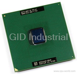
Pentium III Processor - 1 GHz, 256 KB L2 Cache, 100 MHz FSB
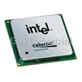
Intel RB80526RY850128 Processor - Intel Celeron Processor Family 850 MHz

Intel RH80536GE0412M Processor - Intel Pentium M Processor 760, Micro-FCPGA, SL7SM, 533 MHz, 2MB L2 ...
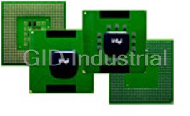
Intel RJ80536GC0292M Processor - INTEL CPU Pentium Mobile 735 1.70AGHz FSB400MHz 2MB uFCBGA Tray
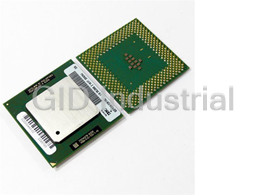
Intel RK30530KZ017512 Processor - 1.40 GHz, 133 MHz, 512 KB, 370 pin, SL6BY, Intel Pentium 3 Process...
Request a Quote

The quote request has been received
Close

Facing challenges or have inquiries? Feel free to contact us!
Call Us +1-469-283-2440
What they say about us
FANTASTIC RESOURCE
One of our top priorities is maintaining our business with precision, and we are constantly looking for affiliates that can help us achieve our goal. With the aid of GID Industrial, our obsolete product management has never been more efficient. They have been a great resource to our company, and have quickly become a go-to supplier on our list!
Bucher Emhart Glass
EXCELLENT SERVICE
With our strict fundamentals and high expectations, we were surprised when we came across GID Industrial and their competitive pricing. When we approached them with our issue, they were incredibly confident in being able to provide us with a seamless solution at the best price for us. GID Industrial quickly understood our needs and provided us with excellent service, as well as fully tested product to ensure what we received would be the right fit for our company.
Fuji
HARD TO FIND A BETTER PROVIDER
Our company provides services to aid in the manufacture of technological products, such as semiconductors and flat panel displays, and often searching for distributors of obsolete product we require can waste time and money. Finding GID Industrial proved to be a great asset to our company, with cost effective solutions and superior knowledge on all of their materials, it’d be hard to find a better provider of obsolete or hard to find products.
Applied Materials
CONSISTENTLY DELIVERS QUALITY SOLUTIONS
Over the years, the equipment used in our company becomes discontinued, but they’re still of great use to us and our customers. Once these products are no longer available through the manufacturer, finding a reliable, quick supplier is a necessity, and luckily for us, GID Industrial has provided the most trustworthy, quality solutions to our obsolete component needs.
Nidec Vamco
TERRIFIC RESOURCE
This company has been a terrific help to us (I work for Trican Well Service) in sourcing the Micron Ram Memory we needed for our Siemens computers. Great service! And great pricing! I know when the product is shipping and when it will arrive, all the way through the ordering process.
Trican Well Service
GO TO SOURCE
When I can't find an obsolete part, I first call GID and they'll come up with my parts every time. Great customer service and follow up as well. Scott emails me from time to time to touch base and see if we're having trouble finding something.....which is often with our 25 yr old equipment.
ConAgra Foods