

 Manufacturers
INTEL LM440LX

Description
Intel LM440LX CPU Board - Slot 1 (BLKLM440LX) Motherboard
Part Number
LM440LX
Price
Request Quote
Manufacturer
INTEL
Lead Time
Request Quote
Category
PRODUCTS - L
Specifications
Audio Output Type
Sound card
Chipset Type
Intel 440LX
Compliant Standards
MPU-401, Microsoft WSS 1.0/2.0, Sound Blaster, Sound Blaster 16/Pro
Plug and Play
CPU Socket Type
Slot 1
CPU Type
Celeron, Pentium II
Data Bus Speed
66 MHz
Form Factor
NLX
Graphics Controller
CL-GD5465
Installed Qty (Max Supported)
1
Interfaces
1 x audio - output - mini-phone 3.5 mm, 1 x display / video - VGA - 15 pin D-Sub (DB-15), 1 x keyboard - generic - 6 pin mini-DIN (PS/2 style), 1 x microphone - input - mini-phone mono 3.5 mm, 1 x mouse - generic - 6 pin mini-DIN (PS/2 style), 1 x parallel - IEEE 1284 (EPP/ECP) - 25 pin D-Sub (DB-25), 1 x storage - floppy interface - 34 pin IDC, 2 x USB - 4 pin USB Type A, 2 x serial - RS-232 - 9 pin D-Sub (DB-9)
Manufacturer
Intel
Model
LM440LX
MPN
BLKLM440LX
Processor
Intel Pentium II
Product Type
Motherboard
Storage Controllers
ATA-33
Storage Interfaces
ATA-33 - connector(s): 2 x 40pin IDC
Supported RAM Integrity Check
ECC, Non-ECC
Supported RAM Technology
SDRAM
Features
- Celeron
- Intel 440LX
- NLX
- Pentium II
- Slot 1
Datasheet

Extracted Text
LM440LX
NLX Motherboard
Technical Product Specification
October 1997
Order Number 685521-001
The LM440LX NLX motherboard may contain design defects or errors known as errata which may cause the product to deviate from published specifications. Current
characterized errata are documented in the LM440LX NLX Motherboard Specification Update.
Revision History
Revision Revision History Date
-001 First release of LM440LX Technical Product Specification. October 1997
This product specification applies only to standard LM440LX motherboards with BIOS identifier
4L4ML0X0.86A.
Changes to this specification will be published in the LM440LX Motherboard Specification
Update before being incorporated into a revision of this document.
Information in this document is provided in connection with Intel products. No license, express or implied, by estoppel or
otherwise, to any intellectual property rights is granted by this document. Except as provided in Intel’s Terms and Conditions of
Sale for such products, Intel assumes no liability whatsoever, and Intel disclaims any express or implied warranty, relating to
sale and/or use of Intel products including liability or warranties relating to fitness for a particular purpose, merchantability, or
infringement of any patent, copyright or other intellectual property right. Intel products are not intended for use in medical, life
saving, or life sustaining applications.
Intel retains the right to make changes to specifications and product descriptions at any time, without notice.
The LM440LX motherboard may contain design defects or errors known as errata which may cause the product to deviate from
published specifications. Current characterized errata are available on request.
Contact your local Intel sales office or your distributor to obtain the latest specifications before placing your product order.
‡
Wake on LAN is a trademark of IBM Corporation.
†
Third-party brands and names are the property of their respective owners.
Copies of documents which have an ordering number and are referenced in this document, or other Intel literature, may be
obtained from:
Intel Corporation
P.O. Box 7641
Mt. Prospect, IL 60056-7641
or call in North America 1-800-879-4683, Europe 44-0-1793-431-155, France 44-0-1793-421-777,
Germany 44-0-1793-421-333, other Countries 708-296-9333.
Copyright 1997, Intel Corporation. All Rights Reserved.
ii
Contents
1 Motherboard Description
1.1 Overview .....................................................................................................................7
1.2 Form Factor................................................................................................................. 9
1.3 I/O Shield .................................................................................................................. 10
1.4 Microprocessor.......................................................................................................... 11
1.4.1 Microprocessor Packaging.......................................................................... 11
1.4.2 Second Level Cache................................................................................... 11
1.4.3 Microprocessor Upgrades ........................................................................... 11
1.5 Memory ..................................................................................................................... 12
1.5.1 Main Memory .............................................................................................. 12
1.5.2 ECC Memory............................................................................................... 12
1.6 AGPset...................................................................................................................... 13
1.6.1 Intel 82443LX PCI/A.G.P. Controller (PAC) ................................................ 13
1.6.2 Intel 82371AB PCI ISA IDE Xcelerator (PIIX4) ........................................... 14
1.6.3 Accelerated Graphics Port (A.G.P.) ............................................................ 15
1.6.4 Universal Serial Bus (USB) ......................................................................... 16
1.6.5 IDE Support ................................................................................................ 16
1.6.6 Real-time Clock, CMOS SRAM, and Battery............................................... 16
1.7 I/O Interface Controller.............................................................................................. 17
1.7.1 Serial Ports ................................................................................................. 17
1.7.2 Parallel Port ................................................................................................ 17
1.7.3 Floppy Controller......................................................................................... 17
1.7.4 PS/2 Keyboard and Mouse Interface .......................................................... 18
1.8 Audio Subsystem ...................................................................................................... 18
1.8.1 OPL3-SA3 Audio System............................................................................ 18
1.8.2 Audio Subsystem Resources...................................................................... 19
1.8.3 Audio Drivers and Utilities ........................................................................... 19
1.8.4 Audio Connectors ....................................................................................... 20
1.9 Hardware Monitor...................................................................................................... 20
1.10 Motherboard Connectors........................................................................................... 21
1.11 Back Panel Connectors............................................................................................. 22
1.12 Configuration Jumpers .............................................................................................. 23
1.12.1 Mic In Select (J8H1).................................................................................... 24
1.12.2 Normal Mode (J6C1)................................................................................... 24
1.12.3 Configuration Mode (J6C1)......................................................................... 24
1.12.4 Recovery Mode (J6C1) ............................................................................... 24
1.13 NLX Card Edge Connectors...................................................................................... 25
1.13.1 NLX Riser with Supplemental Connector.................................................... 26
1.14 Reliability................................................................................................................... 27
1.15 Environmental ........................................................................................................... 27
1.16 Power Consumption.................................................................................................. 28
1.16.1 Power Supply Considerations..................................................................... 28
1.17 Regulatory Compliance ............................................................................................. 29
1.17.1 Product Certification Markings .................................................................... 29
iii
Contents
2 Motherboard Resources
2.1 Memory Map ............................................................................................................. 31
2.2 DMA Channels .......................................................................................................... 31
2.3 I/O Map ..................................................................................................................... 32
2.4 PCI Configuration Space Map................................................................................... 34
2.5 Interrupts...................................................................................................................34
2.6 PCI Interrupt Routing Map......................................................................................... 34
3 Overview of BIOS Features
3.1 Introduction ............................................................................................................... 37
3.2 BIOS Upgrades ......................................................................................................... 37
3.3 BIOS Flash Memory Organization............................................................................. 38
3.4 Plug and Play: PCI Autoconfiguration ...................................................................... 38
3.5 PCI IDE Support........................................................................................................ 38
3.6 ISA Plug and Play ..................................................................................................... 39
3.7 ISA Legacy Devices .................................................................................................. 39
3.8 Desktop Management Interface (DMI) ...................................................................... 40
3.9 Advanced Power Management (APM) ...................................................................... 40
3.10 Language Support..................................................................................................... 41
3.11 Boot Options ............................................................................................................. 41
3.12 OEM Logo or Scan Area ........................................................................................... 41
3.13 USB Legacy Support................................................................................................. 42
3.14 BIOS Setup Access................................................................................................... 43
3.15 Recovering BIOS Data.............................................................................................. 43
4 BIOS Setup Program
4.1 Maintenance Menu.................................................................................................... 45
4.2 Main Menu ................................................................................................................ 46
4.2.1 Floppy Options Submenu ........................................................................... 47
4.2.2 IDE Device Configuration Submenus.......................................................... 48
4.3 Advanced Menu ........................................................................................................ 49
4.3.1 Resource Configuration Submenu.............................................................. 50
4.3.2 Peripheral Configuration Submenu............................................................. 50
4.3.3 Keyboard Configuration Submenu.............................................................. 52
4.3.4 Video Configuration Submenu .................................................................... 52
4.3.5 DMI Event Logging Submenu ..................................................................... 52
4.4 Security Menu ........................................................................................................... 53
4.5 Power Menu .............................................................................................................. 53
4.6 Boot Menu................................................................................................................. 54
4.6.1 Hard Drive Submenu................................................................................... 55
4.6.2 Removable Devices Submenu.................................................................... 55
4.7 Exit Menu .................................................................................................................. 55
iv
Contents
5 Error Messages and Beep Codes
5.1 BIOS Error Messages................................................................................................ 57
5.2 Port 80h POST Codes............................................................................................... 58
5.3 BIOS Beep Codes..................................................................................................... 63
6 Specifications and Customer Support
6.1 Online Support .......................................................................................................... 65
6.2 Specifications ............................................................................................................ 65
Figures
1. Motherboard Components........................................................................................... 8
2. Motherboard Dimensions ............................................................................................ 9
3. Back Panel I/O Shield Dimensions............................................................................ 10
4. Motherboard Connectors........................................................................................... 21
5. Back Panel I/O Connectors....................................................................................... 22
6. Jumper Locations...................................................................................................... 23
Tables
1. Supported Drivers and Resolutions........................................................................... 15
2. Audio Subsystem Resources .................................................................................... 19
3. Fan connector (J3A1)................................................................................................ 21
4. Jumper Settings ........................................................................................................ 23
5. Signals, NLX Riser with Supplemental Connector (P9J1) ......................................... 26
6. Motherboard Environmental Specifications ............................................................... 27
7. Power Usage............................................................................................................. 28
8. Safety Regulations .................................................................................................... 29
9. EMI Regulations........................................................................................................ 29
10. Memory Map ............................................................................................................. 31
11. DMA Channels .......................................................................................................... 31
12. I/O Map ..................................................................................................................... 32
13. PCI Configuration Space Map................................................................................... 34
14. Interrupts...................................................................................................................34
15. PCI Interrupt Routing Map......................................................................................... 35
16. Flash Memory Organization ...................................................................................... 38
17. Recommendations for Configuring an ATAPI Device................................................ 39
18. Setup Menu Bar ........................................................................................................ 45
19. Setup Function Keys ................................................................................................. 45
20. Maintenance Menu.................................................................................................... 46
21. Main Menu ................................................................................................................ 46
22. Floppy Options Submenu.......................................................................................... 47
23. IDE Device Configuration Submenus........................................................................ 48
24. Advanced Menu ........................................................................................................ 49
25. Resource Configuration Submenu ............................................................................ 50
v
Contents
26. Peripheral Configuration Submenu ........................................................................... 51
27. Keyboard Configuration Submenu ............................................................................ 52
28. Video Configuration Submenu .................................................................................. 52
29. DMI Event Logging Submenu ................................................................................... 52
30. Security Menu ........................................................................................................... 53
31. Power Menu .............................................................................................................. 53
32. Boot Menu................................................................................................................. 54
33. Hard Drive Submenu................................................................................................. 55
34. Removable Devices Submenu .................................................................................. 55
35. Exit Menu .................................................................................................................. 55
36. BIOS Error Messages ............................................................................................... 57
37. Port 80h Codes ......................................................................................................... 58
38. Beep Codes .............................................................................................................. 63
39. Compliance with Specifications................................................................................. 65
vi
1 Motherboard Description
1.1 Overview
®
The LM440LX motherboard supports Pentium II family microprocessors operating at 233, 266,
and 300 MHz. The motherboard features:
• NLX form factor
• Minimal jumper design
Main Memory
• Two 168-pin DIMM sockets
• Support for up to 256 MB of synchronous DRAM (SDRAM)
• Support for 66 MHz SDRAM
AGPset and PCI Interface
• Intel 82440LX AGPset PCI/A.G.P Controller (PAC)
• Integrated PCI bus mastering controller using PIIX4
I/O Features
• SMC FDC37C677 I/O controller integrates standard I/O functions: floppy drive interface, one
multi-mode parallel port, two FIFO serial ports, real-time clock, and keyboard and mouse
controller
• Support for two Universal Serial Bus (USB) ports
• Dual channel Fast IDE interface
Audio Subsystem
• Yamaha OPL3-SA3 audio codec component
Graphics Subsystem
†
• Cirrus Logic CL-GD5465 A.G.P. graphics accelerator with 4 MB of (RDRAM) RAMBUS
video memory
Other features
• Plug and Play compatible
• Support for Advanced Configuration and Power Interface (ACPI) and Advanced Power
Management (APM)
Software drivers and utilities are available from Intel.
7
Motherboard Description
Figure 1 shows the general location of the components on the motherboard.
A
B
C
R
Q
D
P
E
F
G
O
H
I
J
N M L K
OM06340a
A Back panel connectors J NLX riser edge connector
B Supplemental edge connector K National Semiconductor LM79 hardware monitor
C SMC FDC37C677 I/O controller L Slot 1 connector
D Microphone input select jumper M Fan connector
E Yamaha OPL3-SA3 audio codec N Intel 82443LX PCI/A.G.P. controller
F Flash memory O DIMM sockets
G Intel 82371AB PCI ISA IDE Xcelerator (PIIX4) P Cirrus Logic CL-GD5465 A.G.P. graphics
accelerator
H Configuration jumper Q Battery
I Speaker R RAMBUS memory
Figure 1. Motherboard Components
8
LM440LX NLX Motherboard Technical Product Specification
1.2 Form Factor
The motherboard is designed to fit into a standard NLX form factor chassis. Figure 2 illustrates the
mechanical form factor for the motherboard. Location of the I/O connectors, riser connector, and
mounting holes is in strict compliance with the NLX I/O Shield Design Suggestions specification
(see Section 6.2).
6.05
9.80
8.70
6.225
0.00
0.20
7.80
0.45
3.40 7.34
0.00
OM06337a
Figure 2. Motherboard Dimensions
9
Motherboard Description
1.3 I/O Shield
The back panel I/O shield for the motherboard must meet specific dimensional and material
requirements. Computers built with this motherboard need the I/O shield to pass EMI certification
testing. Figure 3 shows the critical dimensions for the I/O shield and indicates the position of each
cutout. For more chassis design requirements, see the NLX specification (see Section 6.2).
0.543
1.752
0.208
1.197
0.948
0.530
0.456
0.447
0.00
0.143
0.456
0.366(2) 0.490(2)
OM06463
Figure 3. Back Panel I/O Shield Dimensions
10
0.168
0.00
0.570
1.175
1.838
2.504
3.179
4.532
4.637
5.997
7.274
7.429
7.908
8.853
LM440LX NLX Motherboard Technical Product Specification
1.4 Microprocessor
The motherboard supports a single Pentium II processor. The processor’s VID pins automatically
program the motherboard’s voltage regulator to the required processor voltage. The motherboard
operates with processors that run internally at 233, 266, or 300 MHz and run externally at 66 MHz
host bus speed with either a 256 KB or 512 KB second-level cache.
The processor implements MMX technology and maintains full backward compatibility with the
8086, 80286, Intel386, Intel486, and Pentium processor. The processor’s numeric coprocessor
significantly increases the speed of floating-point operations and complies with ANSI/IEEE
standard 754-1985.
1.4.1 Microprocessor Packaging
The processor is packaged in a Single Edge Contact (S.E.C.) cartridge. The S.E.C. cartridge
includes the processor core, the second-level cache, a thermal plate, and a back cover.
The processor connects to the motherboard through the Slot 1 processor connector, a 242-pin edge
connector. When mounted in Slot 1, the processor is secured by a retention mechanism attached to
the motherboard. The processor’s heatsink is stabilized by a heatsink support that is attached to the
motherboard.
1.4.2 Second Level Cache
The second-level cache is located on the substrate of the S.E.C. cartridge. The cache includes burst
pipelined synchronous static RAM (BSRAM) and tag RAM. There can be two or four BSRAM
components totaling 256 KB or 512 KB in size. All supported onboard memory can be cached.
1.4.3 Microprocessor Upgrades
The motherboard can be upgraded with Pentium II processors that run at higher processor speeds.
When upgrading the processor, use the BIOS configuration mode to change the processor. See
Section 1.12.3 for information about configuration mode.
11
Motherboard Description
1.5 Memory
1.5.1 Main Memory
The motherboard has two dual inline memory module (DIMM) sockets. Minimum memory size is
16 MB; maximum memory size is 256 MB. The BIOS automatically detects memory type, size,
and speed.
The motherboard supports the following memory features:
• 168-pin DIMMs with gold-plated contacts
• 66 MHz SDRAM only
• Non-ECC (64-bit) and ECC (72-bit) memory
• 3.3 V memory only
• Single- or double-sided DIMMs in the following sizes:
DIMM Size Non-ECC Configuration ECC Configuration
16 MB 2 Mbit x 64 2 Mbit x 72
32 MB 4 Mbit x 64 4 Mbit x 72
64 MB 8 Mbit x 64 8 Mbit x 72
128 MB 16 Mbit x 64 16 Mbit x 72
Memory can be installed in one or two sockets. Memory size can vary between sockets.
NOTE
�
To function properly, SDRAM DIMMs must meet the Intel 4-clock, 66 MHz, unbuffered SDRAM
specification for either 64-bit or 72-bit SDRAM. See Section 6.2 for information about these
specifications.
1.5.2 ECC Memory
Error checking and correcting (ECC) memory detects multiple-bit errors and corrects single-bit
errors. When ECC memory is installed, the BIOS supports both ECC and non-ECC mode. ECC
mode is enabled in the Setup program. The BIOS automatically detects if ECC memory is
installed and provides the Setup option for selecting ECC mode. If any non-ECC memory is
installed, the Setup option for ECC mode does not appear.
The following table describes the effect of using Setup to put each memory type in each supported
mode. Whenever ECC mode is selected in Setup, some performance loss occurs.
Memory Error Detection Mode Established in Setup Program
ECC Disabled ECC Enabled
No error detection N/A
Non-ECC DIMM
No error detection Single-bit error correction, multiple-bit error
ECC DIMM
detection
12
LM440LX NLX Motherboard Technical Product Specification
1.6 AGPset
The Intel 440LX AGPset is designed for the Pentium II processor. It consists of the Intel 82443LX
PCI/A.G.P. controller (PAC) and the Intel 82371AB PCI/ISA IDE Xcelerator (PIIX4) bridge chip.
1.6.1 Intel 82443LX PCI/A.G.P. Controller (PAC)
The PAC provides bus-control signals, address paths, and data paths for transfers between the
processor’s host bus, PCI bus, Accelerated Graphics Port (A.G.P.), and main memory. The PAC
features:
• Processor interface control
Processor host bus speed of 66 MHz
32-bit addressing
GTL+ compliant host bus
• Integrated DRAM controller
Supports synchronous DRAM (SDRAM)
64/72-bit path-to-memory
Auto detection of memory type
Supports 4-, 16-, 64-Mbit DRAM devices
Symmetrical and asymmetrical DRAM addressing
Supports 3.3 V DRAMs
• Accelerated Graphics Port Interface
Complies with A.G.P. specification (see Section 6.2 for specification information)
Supports 3.3 V A.G.P. devices with data transfer rates up to 66 MHz
Synchronous coupling to the host-bus frequency
• Fully-synchronous PCI bus interface
Complies with PCI specification (see Section 6.2 for specification information)
PCI-to-DRAM access greater than 100 MB/sec
Supports five PCI bus masters in addition to the host and PCI-to-ISA I/O bridge
Delayed transactions
PCI parity checking and generation support
• Data Buffering
Host-to-DRAM, PCI-to-DRAM, and A.G.P.-to-DRAM write-data buffering
Write-combining for host-to-PCI burst writes
Supports concurrent host, PCI, and A.G.P. transactions to main memory
• Supports system management mode (SMM)
13
Motherboard Description
1.6.2 Intel 82371AB PCI ISA IDE Xcelerator (PIIX4)
The PIIX4 is a multifunction PCI device implementing the PCI-to-ISA bridge, PCI IDE
functionality, Universal Serial Bus (USB) host/hub function, and enhanced power management.
The PIIX4 features:
• Multifunction PCI-to-ISA bridge
Supports the PCI bus at 33 MHz
Complies with PCI specification (see Section 6.2 for specification information)
Full ISA or extended I/O (EIO) bus support
• USB controller
Two USB ports (see Section 6.2 for compliance level)
Supports legacy keyboard and mouse
Supports universal host controller interface (UHCI) design guide revision 1.1 interface
• Integrated dual-channel enhanced IDE interface
Supports up to four IDE devices
PIO Mode 4 transfers at up to 14 MB/sec
Supports Ultra DMA/33 synchronous DMA mode transfers up to 33 MB/sec
Bus master mode with an 8 x 32-bit buffer for bus master PCI IDE burst transfers
• Enhanced DMA controller
Two 8237-based DMA controllers
Supports PCI DMA with three PC/PCI channels and distributed DMA protocols
Fast type-F DMA for reduced PCI bus usage
• Interrupt controller based on 82C59
Supports 15 interrupts
Programmable for edge/level sensitivity
• Power management logic
Sleep/resume logic
Supports thermal alarm
Supports wake-on-modem through Ring Indicate input
‡
Supports Wake on LAN
• Real-time Clock
256 byte battery-backed CMOS SRAM
Includes date alarm
• 16-bit counters/timers based on 82C54
14
LM440LX NLX Motherboard Technical Product Specification
1.6.3 Accelerated Graphics Port (A.G.P.)
A.G.P. is a high-performance interconnect for graphic-intensive applications, such as 3D
applications. A.G.P. is independent of the PCI bus and is intended for exclusive use with
graphical-display devices. A.G.P. provides these performance features:
• Pipelined-memory read and write operations that hide memory access latency
• Demultiplexing of address and data on the bus for near 100% bus efficiency
• AC timing for 66 MHz data transfer rates, allowing data throughput of 250 MB/sec
A.G.P. complies with the 66 MHz PCI specification. See Section 6.2 for information about the
A.G.P. and PCI specifications.
1.6.3.1 Cirrus Logic CL-GD5465 A.G.P. graphics accelerator
The CL-GD5465 supports A.G.P. for higher bandwidth between the system memory and the
graphics subsystem. It is a member of the Laguna family of RAMBUS-based graphics
accelerators, offering 3D-graphics capability while maintaining a high level of 2D performance.
The features include:
• 64-bit graphics engine with integrated 3D game acceleration
• High-performance 64-bit GUI accelerator
• Video playback acceleration
†
• Integrated VGA controller
• Integrated 230-MHz palette DAC and clock synthesizer
Table 1. Supported Drivers and Resolutions
8 bit 16 bit 24 bit 32 bit
Drivers 256 colors 65,536 colors 16,777,216 colors 16,777,216 colors
†
Microsoft Windows 640 x 480 640 x 480 640 x 480 640 x 480***
Microsoft DCI* Provider 800 x 600 800 x 600 800 x 600 800 x 600***
Microsoft Windows 95 1024 x 768 1024 x 768 1024 x 768 1024 x 768***
Microsoft DirectDraw 1280 x 1024 1280 x 1024
†
AutoCAD 1600 x 1200
AutoShade with Renderman
3D Studio MicroStation
†
Microsoft Windows NT
† †
OS/2 v3.x, Warp 640 x 480 640 x 480
800 x 600 800 x 600
1024 x 768 1024 x 768
1280 x 1024
VPM** Resolution-independent
* Display control interface
** Video port manager
*** Microsoft Windows NT only
15
Motherboard Description
1.6.4 Universal Serial Bus (USB)
The motherboard has two USB ports. The motherboard fully supports the universal host controller
interface (UHCI) and uses UHCI-compatible software drivers. See Section 6.2 for information
about the USB specification. USB features include:
• Self-identifying peripherals that can be plugged in while the computer is running
• Automatic mapping of function to driver and configuration
• Isochronous and asynchronous transfer types supported over the same set of wires
• Up to 127 physical devices supported
• Guaranteed bandwidth and low latencies appropriate for telephony, audio, and other
applications
• Error-handling and fault-recovery mechanisms built into the protocol
NOTE
�
Computer systems that have an unshielded cable attached to a USB port may not meet FCC
Class B requirements, even if no device or a low-speed USB device is attached to the cable. Use
shielded cable that meets the requirements for full-speed devices.
1.6.5 IDE Support
The motherboard has two independent bus-mastering PCI IDE interfaces. These interfaces support
PIO Mode 3, PIO Mode 4, ATAPI devices (e.g., CD-ROM), and Ultra DMA/33 synchronous-
DMA mode transfers. The IDE interface signals are routed to the NLX riser connector.
The BIOS supports logical block addressing (LBA) and extended cylinder head sector (ECHS)
translation modes. The BIOS automatically detects the IDE device transfer rate and translation
mode.
Programmed I/O operations usually require a substantial amount of processor bandwidth.
However, in multitasking operating systems, the bandwidth freed by bus mastering IDE can be
devoted to other tasks while disk transfers are occurring.
1.6.6 Real-time Clock, CMOS SRAM, and Battery
The real-time clock is compatible with DS1287 and MC146818 components. The clock provides a
time-of-day clock and a multi-century calendar with alarm features and century rollover. The real-
time clock supports 256 bytes of battery-backed CMOS SRAM in two banks that are reserved for
BIOS use.
The time, date, and CMOS values can be specified in the Setup program. The CMOS values can
be returned to their defaults by using the Setup program.
An external coin-cell battery powers the real-time clock and CMOS memory. When the computer
is not plugged into a wall socket, the battery has an estimated life of three years. When the
computer is plugged in, the 3 V standby current from the power supply extends the life of the
battery. The clock is accurate to ± 13 minutes/year at 25 ºC with 5 V applied.
16
LM440LX NLX Motherboard Technical Product Specification
1.7 I/O Interface Controller
The motherboard uses the SMC FDC37C677 I/O controller which features:
• ISA Plug-and-Play compatible register set
• Two serial ports
• FIFO support on both serial and floppy interfaces
• One parallel port with ECP and EPP support
†
• PS/2 style mouse and keyboard interfaces
• Supports BIOS setup for various configuration options
1.7.1 Serial Ports
The motherboard has two 9-pin D-Sub serial port connectors located on the back panel. The
NS16C550-compatible UARTs support data transfers at speeds up to 115.2 Kbits/sec with BIOS
support.
1.7.2 Parallel Port
The connector for the multimode bidirectional parallel port is a 25-pin D-Sub connector located on
the back panel of the motherboard. In the Setup program, there are four options for parallel port
operation:
• Compatible (standard mode)
• Bidirectional (PS/2 compatible)
• Bidirectional Enhanced Parallel Port (EPP). A driver from the peripheral manufacturer is
required for operation. See Section 6.2 for EPP compatibility.
• Bidirectional high-speed Extended Capabilities Port (ECP)
1.7.3 Floppy Controller
The I/O controller is software compatible with the DP8473 and 82077 floppy drive controllers. In
the Setup program, the floppy interface can be configured for the following floppy drive capacities
and sizes:
• 360 KB, 5.25-inch
• 1.2 MB, 5.25-inch
• 720 KB, 3.5-inch
• 1.2 MB, 3.5-inch (Mode 3 floppy support, driver required)
• 1.25/1.44 MB, 3.5-inch
• 2.88 MB, 3.5-inch
• 120 MB (LS-120)
The floppy disk interface signals are routed to the NLX riser connector.
17
Motherboard Description
1.7.4 PS/2 Keyboard and Mouse Interface
PS/2 keyboard and mouse connectors are located on the back panel of the motherboard. The +5 V
†
lines to these connectors are protected with a PolySwitch circuit that, like a self-healing fuse,
reestablishes the connection after an over-current condition is removed. While this device
eliminates the possibility of having to replace a fuse, power to the computer should be turned off
before connecting or disconnecting a keyboard or mouse.
NOTE
�
You can plug the mouse and keyboard into either PS/2 connector.
The keyboard controller contains code which provides the traditional keyboard and mouse control
functions, and also supports Power On/Reset password protection. A Power On/Reset password
can be specified in the Setup program.
The keyboard controller also supports the hot-key sequence , software reset.
This key sequence resets the computer’s software by jumping to the beginning of the BIOS code
and running the Power On Self Test (POST).
1.8 Audio Subsystem
1.8.1 OPL3-SA3 Audio System
The onboard audio subsystem features the Yamaha OPL3-SA3 (YMF715) device. The features of
the device include:
• A 16-bit audio codec
• OPL3 FM synthesis
• An integrated 3D enhanced stereo controller
• Support for MPU-401
• Stereo analog-to-digital and digital-to-analog converters
• Analog mixing, anti-aliasing, and reconstruction filters
• 16-bit address decoding supported
• Line, microphone, and monaural inputs
• ADPCM, A-law, or μlaw digital audio compression and decompression
• Full digital control of all mixer and volume control functions
• Microphone input (Mic In) connector is jumper selectable between the back panel and the riser
• Plug and Play compatible
†
• Sound Blaster Pro and Microsoft Windows Sound System compatible
18
LM440LX NLX Motherboard Technical Product Specification
1.8.2 Audio Subsystem Resources
The following table shows the IRQ, DMA channel, and base I/O address options for the audio
subsystem. Options are listed in order of preference specified by Yamaha. These options are
automatically chosen by the Plug and Play interface, so there are no default settings. Onboard
audio can be enabled or disabled in the Setup program.
Table 2. Audio Subsystem Resources
IRQ DMA channel I/O Address
Resource (Options) (Options) (Options)
†
Sound Blaster 5, 7, 10, 11 0, 1, 3 220-22Fh
(DMA playback, DMA shared with
240-24Fh
Windows Sound System capture)
16 bytes on 16-byte
boundary in the
(5 is recommended)
range of 220-280h
Windows Sound System 5, 7, 10, 11 0, 1, 3 530-537h
(DMA playback)
E80-E87h
8 bytes on 8-byte
boundary in the
range of 530-F48h
MPU-401 330-331h
(IRQ shared with Sound Blaster)
300-301h
2 bytes on 2-byte
boundary in the
range of 300-334h
†
AdLib 388-38Dh
6 bytes on 8-byte
boundary in the
range of 388-3F8h
1.8.3 Audio Drivers and Utilities
Audio software and utilities are available from Intel’s World Wide Web site (see Section 6.2).
Audio driver support is provided for the Microsoft Windows 3.1, Microsoft Windows 95,
Microsoft Windows NT (versions 3.51 and 4.0), and IBM OS/2 Warp (versions 3.0 and 4.0)
operating systems.
19
Motherboard Description
1.8.4 Audio Connectors
The back panel includes the following audio connectors:
• Line Out
• Mic In
1.9 Hardware Monitor
The optional hardware monitor component (National Semiconductor LM79) provides low-cost
instrumentation capabilities designed to reduce the total cost of owning a PC when used with
®
LANDesk Client Manager. The hardware implementation is a single-chip ASIC. Features
include:
• An integrated ambient temperature sensor
• Fan speed sensors
• Power supply voltage monitoring to detect levels above or below acceptable values
• Remote reset capabilities from a remote peer or server through LANDesk Client Manager,
Version 3.0 and service layers (when available)
When suggested ratings for temperature, fan speed, or voltage are exceeded, an interrupt is
activated. The hardware monitor component (LM79) connects to the system management bus. For
more information on the LM79, see http://www.national.com.
20
LM440LX NLX Motherboard Technical Product Specification
1.10 Motherboard Connectors
Figure 4 shows the connectors on the motherboard.
A
E
B
1
D C
3
OM06341a
A Supplemental connector D Fan connector
B Riser connector E DIMM sockets
C CPU slot
Figure 4. Motherboard Connectors
Table 3. Fan connector (J3A1)
Pin Signal Name
1 GND
2 +12V
3 Tachometer
21
Motherboard Description
1.11 Back Panel Connectors
Figure 5 shows the back panel I/O connectors.
H
DE F G I
A B C
OM06338a
A Microphone Input F Serial Port B
B Line Out G Serial Port A
C USB H Parallel Port
D Mouse/ Keyboard I VGA Video
E Mouse/ Keyboard
Figure 5. Back Panel I/O Connectors
22
LM440LX NLX Motherboard Technical Product Specification
1.12 Configuration Jumpers
Figure 6 shows the location of the microphone input and configuration jumper blocks on the
motherboard.
3
A
1
J8H1
3
B
1
J6C1
OM06339a
A Microphone input select jumper B Configuration jumper
Figure 6. Jumper Block Locations
Table 4. Jumper Settings
Function Jumper Block Configuration
Mic In Selection J8H1 1-2 Front panel Mic In
2-3 Back panel Mic In (default)
Configuration J6C1 Normal (default)
1-2
2-3 Configure
none Recovery
CAUTION
Do not move any of the jumpers with the power on. Always turn off the power and unplug the
power cord from the computer before changing jumpers. Changing the jumper settings when the
power is off ensures that the changes will be recognized.
23
Motherboard Description
1.12.1 Mic In Selection
Connect pins 1-2 with a jumper on the Mic In selection jumper block (J8H1) to route the Mic In
input through the riser and disable Mic In through the back panel. Connect pins 2-3 with a jumper
on the Mic In selection jumper block to route the Mic In input through the back panel and disable
Mic In through the riser.
1.12.2 Normal Mode
This mode is for normal computer booting and operations. Connect pins 1 and 2 with a jumper on
the configuration jumper block (J6C1) to enable this mode. The BIOS uses the current
bus/processor frequency ratio, configuration information, and passwords to boot the computer.
Access to the Setup program can be restricted using a supervisor or user password.
In normal mode, the BIOS attempts an automatic recovery if the configuration information in
CMOS RAM is corrupted.
1.12.3 Configure Mode
This mode is for configuring special BIOS settings, including processor speed and special
maintenance options. This mode is used when upgrading the BIOS, upgrading the processor, or
clearing the passwords. Connect pins 2 and 3 with a jumper on the configuration jumper block
(J6C1) to enable this mode. In this mode, Setup automatically executes after the POST runs. No
password is required, and this mode overrides any passwords that are set. The Maintenance menu
is the first menu displayed. This menu provides options for setting the processor speed and
clearing passwords. All other Setup screens are available. Configure mode uses the default BIOS
settings for booting, not the current user or supervisor settings. The default settings include using
the lowest bus/processor frequency ratio the processor supports. User and supervisor settings are
preserved and used when the computer is rebooted.
For the configuration changes to take effect after exiting the Setup program, power down the
computer, set the configuration jumper to normal mode (see Section 1.12.2), and boot the
computer.
In configure mode, the BIOS attempts an automatic recovery if the configuration information
CMOS RAM is corrupted.
1.12.4 Recovery Mode
This mode is for upgrading the BIOS or recovering BIOS data. Remove the jumper (no pins
connected) on the configuration jumper block (J6C1). After the computer is powered-on, the BIOS
attempts to upgrade or recover the BIOS data from a floppy diskette in the floppy drive. If a
diskette is not in the boot drive, the BIOS runs the POST, does not boot the operating system, and
displays a message that the jumper is not properly installed. If the recovery fails with a diskette in
the boot drive, a continuous, low-pitched, single beep indicates that the recovery failed.
For the configuration changes to take effect after a successful recovery, power down the computer,
set the configuration jumper to normal mode (see Section 1.12.2), and boot the computer.
24
LM440LX NLX Motherboard Technical Product Specification
1.13 NLX Card Edge Connectors
The NLX riser connector on the motherboard consists of a 340 (2x170) position and a 26 (2x13)
supplemental position gold finger contact. All edge connector pin definitions are defined in the
NLX specification, version 1.2 (see Section 6.2).
The motherboard supports the following signals:
• PCI expansion slots
• ISA expansion slots
• IDE headers
• 1 floppy drive header
• Miscellaneous front panel signals including: USB, Mic In, and Line Out
See Table 5 for the supplemental connector signals supported by the motherboard.
NOTE
�
The riser must provide power to the motherboard. For power consumption information, see
Section 1.16.
25
Motherboard Description
1.13.1 NLX Riser with Supplemental Connector
Table 5. Signals, NLX Riser with Supplemental Connector (P9J1)
Pin Signal Name Type I/O * Description Signal Type
X1 CD_IN_LT AUDIO I CD-ROM line in left Analog
1V RMS
X2 AGND PWR NA Low pass filtered ground for audio circuitry on NA
the riser
X3 MIC_IN AUDIO I Pre-amplified microphone input. Pre-amp Analog
circuitry to reside on riser or in microphone 1V RMS
X4 LINE_OUT_LT AUDIO O Analog line out left Analog
1V RMS
X5 FP_SPKR_EN AUDIO I Not Supported TTL
X6 VOL_DN# AUDIO I Not Supported TTL
X7 GND PWR NA Ground NA
X8 SMI# SYS I Not Supported open drain
X9 RESERVED RES NA Reserved NA
X10 RESERVED RES NA Reserved NA
X11 RESERVED RES NA Reserved NA
X12 AGND PWR NA Low pass filtered ground for audio circuitry on NA
the riser
X13 MODEM_MIC AUDIO O Pre-amplified microphone mono output signal Analog
from motherboard to telephony device 1V RMS
Y1 CD_IN_RT AUDIO I CD-ROM line in right Analog
1V RMS
Y2 CD_IN_GND PWR I Isolated CD-ROM Ground NA
Y3 AVCC PWR O Clean power from the motherboard to audio 5-9V DC
circuitry on the NLX riser; could be an
isolated power source; 1.5 Ampere max.
limitation because of the connector / gold
finger limitation
Y4 LINE_OUT_RT AUDIO O Analog line out right Analog
1V RMS
Y5 FP_MIC_EN AUDIO I Not Supported TTL
Y6 VOL_UP# AUDIO I Not Supported TTL
Y7 AC_RST# AC’97 O Not Supported TTL
Y8 AC_SD_IN AC’97 I Not Supported TTL
Y9 GROUND PWR NA Digital (main motherboard) ground plane NA
Y10 AC_SD_OUT AC’97 O Not Supported TTL
Y11 AC_SYNC AC’97 O Not Supported TTL
Y12 AC_BIT_CLK AC’97 I Not Supported TTL
Y13 MODEM_SPKR AUDIO O Analog mono output signal from telephony Analog
device to motherboard 1V RMS
* I/O column: relative to motherboard, “O” = output, from motherboard to riser; “I” = input, from riser to motherboard.
26
LM440LX NLX Motherboard Technical Product Specification
1.14 Reliability
The Mean Time Between Failures (MTBF) data is calculated from predicted data at 55 ºC.
Motherboard MTBF: 131,473 hours
1.15 Environmental
Table 6. Motherboard Environmental Specifications
Parameter Specification
Temperature
Non-Operating -40 °C to +70 °C
Operating 0 °C to +55 °C
Shock
Unpackaged 50 G trapezoidal waveform
Velocity change of 170 inches/second
Packaged Half sine 2 millisecond
Product Weight Free Fall (inches) Velocity Change (inches/sec)
<20 lbs. 36 167
21-40 lbs. 30 152
41-80 lbs. 24 136
81-100 lbs. 18 118
Vibration
Unpackaged 5 Hz to 20 Hz : 0.01g² Hz sloping up to 0.02 g² Hz
20 Hz to 500 Hz : 0.02g² Hz (flat)
Packaged 10 Hz to 40 Hz : 0.015g² Hz (flat)
40 Hz to 500 Hz : 0.015g² Hz sloping down to 0.00015 g² Hz
27
Motherboard Description
1.16 Power Consumption
Table 7 lists power usage for a computer that contains the motherboard, a 266 MHz Pentium II
processor, 32 MB RAM, 512 KB cache, 3.5-inch floppy drive, 1.6 GB IDE hard drive, and a
8X IDE CD-ROM. This information is provided only as a guide for calculating approximate
power usage with additional resources added.
Values for the Windows 95 desktop mode are measured at 1024 x 768 x 16 bit colors and 72 Hz
refresh rate. AC watts are measured with a typical 75 W supply, nominal input voltage and
frequency, with true RMS wattmeter at the line input.
Table 7. Power Usage
DC (amps) at:
Mode AC (watts) +3.3 V +5 V -5 V +12 V -12 V
DOS prompt, APM disabled 47.82 4.23 5.64 0 0.432 0.04
Windows 95 desktop, APM disabled 52.92 4.23 6.64 0 0.44 0.04
(Normal)
Windows 95 desktop, APM enabled, in 41.09 2.22 5.6 0 0.44 0.04
System Management Mode (SMM)
(Suspend)
1.16.1 Power Supply Considerations
For typical configurations, the motherboard is designed to operate with at least a 75 W NLX power
supply (see Section 6.2 for the specification). A higher-wattage power supply should be used for
heavily-loaded configurations. The power supply must comply with the following
recommendations found in the indicated sections of the NLX power supply specification:
• The potential relation between 3.3VDC and +5VDC power rails (Section 4.2)
• The current capability of the +5VSB line (Section 4.2.1.2)
• All timing parameters (Section 4.2.1.3)
• All voltage tolerances (Section 4.2.2)
28
LM440LX NLX Motherboard Technical Product Specification
1.17 Regulatory Compliance
This printed circuit board assembly complies with the following safety and EMI regulations when
correctly installed in a compatible host system.
Table 8. Safety Regulations
Regulation Title
UL 1950 - CSA 950-95, 3rd edition, The Standard for Safety of Information Technology Equipment
Dated 07-28-95 including Electrical Business Equipment. (USA & Canada)
CSA C22.2 No. 950-95 3rd edition, The Standard for Safety of Information Technology Equipment
Dated 07-28-95 including Electrical Business Equipment. (Canada)
EN 60 950, 2nd edition, 1992 (with The Standard for Safety of Information Technology Equipment
Amendments 1, 2 & 3) including Electrical Business Equipment. (European Union)
IEC 950, 2nd edition, 1991 (with The Standard for Safety of Information Technology Equipment
Amendments 1-4) including Electrical Business Equipment. (International)
EMKO-TSE (74-SEC) 207/94 Summary of Nordic deviations to EN 60 950. (Norway, Sweden,
Denmark & Finland)
Table 9. EMI Regulations
Regulation Title
FCC Class B Title 47, Code of Federal Regulations; General rules and regulations, &
Radio Frequency devices. Product compliance is verified using limits
from CISPR 22 (frequencies to 1 GHz) and FCC Rules, Section
15.109(a) (frequencies to 1 GHz) and test criteria as defined in ANSI
C63.4 and Section 15.32 (a) of the FCC Rules.
CISPR 22, 2nd Edition, 1993 Limits and methods of measurement of Radio Interference
Characteristics of Information Technology Equipment. (International)
EN 55 022, 1995 Limits and methods of measurement of Radio Interference
Characteristics of Information Technology Equipment. (Europe)
EN 50 082-1 (1992) Generic Immunity Standard; Currently compliance is determined via
testing to IEC 801-2, -3, and -4. (Europe)
VCCI Class 2 (ITE) Implementation Regulations for Voluntary Control of Radio Interference
by Data Processing Equipment and Electronic Office Machines. (Japan)
ICES-003, Issue 2 Interference-Causing Equipment Standard, Digital Apparatus. (Canada)
1.17.1 Product Certification Markings
This printed circuit board assembly has the following product certification markings:
• European CE Marking: Consists of a marking on the board and shipping container.
• UL Recognition Mark: Consists of the UL File No. E139761 on the component side of the
board and the PB No. on the solder side of the board. Board material flammability is 94V-1
or -0.
• Canadian Compliance: Consists of small c followed by a stylized backward UR on component
side of the board.
29
Motherboard Description
30
2 Motherboard Resources
NOTE
�
For more detailed information about the resources used for onboard audio, see the Audio
Subsystem section in Chapter 1.
2.1 Memory Map
Table 10. Memory Map
Address Range (decimal) Address Range (hex) Size Description
1024 K - 262144 K 100000 - 10000000 255 MB Extended Memory
1008 K - 1024 K FC000 - FFFFF 16 KB Boot block
1000 K - 1008 K FA000 - FBFFF 8 KB ESCD (Plug and Play configuration and DMI)
996 K - 1000 K F9000 - F9FFF 4 KB Reserved for BIOS
992 K - 996 K F8000 - F8FFF 4 KB OEM Logo or Scan User Flash
928 K - 992 K E8000 - F7FFF 64 KB POST BIOS
896 K - 928 K E0000 - E7FFF 32 KB POST BIOS (Available as UMB)
800 K - 896 K C8000 - DFFFF 96 KB Available high DOS memory (open to ISA
and PCI bus)
640 K - 800 K A0000 - C7FFF 160 KB Video memory and BIOS
639 K - 640 K 9FC00 - 9FFFF 1 KB Extended BIOS data (movable by memory
manager software)
512 K - 639 K 80000 - 9FBFF 127 KB Extended conventional memory
0 K - 512 K 00000 - 7FFFF 512 KB Conventional memory
2.2 DMA Channels
Table 11. DMA Channels
DMA Channel Number Data Width System Resource
0 8 or 16 bits Audio
1 8 or 16 bits Audio / Parallel Port
2 8 or 16 bits Floppy Drive
3 8 or 16 bits Parallel Port (for ECP or EPP) / Audio
4 Reserved - Cascade Channel
5 16 bits Open
6 16 bits Open
7 16 bits Open
31
Motherboard Resources
2.3 I/O Map
Table 12. I/O Map
Address (hex) Size Description
0000 - 000F 16 bytes PIIX4- DMA 1
0020 - 0021 2 bytes PIIX4 - interrupt controller 1
002E - 002F 2 bytes I/O controller configuration registers
0040 - 0043 4 bytes PIIX4 - Counter/Timer 1
0048 - 004B 4 bytes PIIX4- Counter/Timer 2
0060 1 byte Keyboard Controller Byte - Reset IRQ
0061 1 byte PIIX4 - NMI, Speaker Control
0064 1 byte Keyboard controller, CMD/STAT Byte
0070, bit 7 1 bit PIIX4 - enable NMI
0070, bits 6:0 7 bits PIIX4 - real time clock, address
0071 1 byte PIIX4 - real time clock, data
0078 1 byte Reserved - motherboard configuration
0079 1 byte Reserved - motherboard configuration
0080 - 008F 16 bytes PIIX4 - DMA page registers
00A0 - 00A1 2 bytes PIIX4 - interrupt controller 2
00B2 - 00B3 2 bytes APM control
00C0 - 00DE 31 bytes PIIX4 - DMA 2
00F0 1 byte Reset numeric error
0170 - 0177 8 bytes Secondary IDE channel
01F0 - 01F7 8 bytes Primary IDE channel
0200 - 0207 8 bytes Audio
0220 - 022F 16 bytes Audio (Sound Blaster compatible)
0240 - 024F 16 bytes Audio (Sound Blaster compatible)
0278 - 027F 8 bytes LPT2
02E8 - 02EF 8 bytes COM4/Video (8514A)
02F8 - 02FF 8 bytes COM2
0300 - 0301 2 bytes MPU-401 (MIDI)
0330 - 0331 2 bytes MPU-401 (MIDI)
0332 - 0333 2 bytes MPU-401 (MIDI)
0334 - 0335 2 bytes MPU-401 (MIDI)
0376 1 byte Secondary IDE channel command port
0377 1 byte Floppy channel 2 command
0377, bit 7 1 bit Floppy disk change, channel 2
0377, bits 6:0 7 bits Secondary IDE channel status port
0378 - 037F 8 bytes LPT1
0388 - 038D 6 bytes AdLib (FM synthesizer)
continued �
32
LM440LX NLX Motherboard Technical Product Specification
(continued)
Table 12. I/O Map
Address (hex) Size Description
03B4 - 03B5 2 bytes Video (VGA)
03BA 1 byte Video (VGA)
03BC - 03BF 4 bytes LPT3
03C0 - 03CA 11 bytes Video (VGA)
03CC 1 byte Video (VGA)
03CE - 03CF 2 bytes Video (VGA)
03D4 - 03D5 2 bytes Video (VGA)
03DA 1 byte Video (VGA)
03E8 - 03EF 8 bytes COM3
03F0 - 03F5 6 bytes Floppy Channel 1
03F6 1 byte Primary IDE channel command port
03F7 (Write) 1 byte Floppy channel 1 command
03F7, bit 7 1 bit Floppy disk change channel 1
03F7, bits 6:0 7 bits Primary IDE channel status port
03F8 - 03FF 8 bytes COM1
04D0 - 04D1 2 bytes Edge/level triggered PIC
0530 - 0537 8 bytes Windows Sound System
0604 - 060B 8 bytes Windows Sound System
LPTn + 400h 8 bytes ECP port, LPTn base address + 400h
0CF8 - 0CFB* 4 bytes PCI configuration address register
0CF9** 1 byte Turbo and reset control register
0CFC - 0CFF 4 bytes PCI configuration data register
0E80 - 0E87 8 bytes Windows Sound System
0F40 - 0F47 8 bytes Windows Sound System
0F86 - 0F87 2 bytes Yamaha OPL3-SA3 configuration
7000 - 700D 14 bytes SM Bus I/O space Registers
8000 - 8037 56 bytes Power Management I/O space Registers
FF00 - FF07 8 bytes IDE bus master register
FFA0 - FFA7 8 bytes Primary bus master IDE registers
FFA8 - FFAF 8 bytes Secondary bus master IDE registers
* DWORD access only
** Byte access only
NOTE
�
See the Audio section(s) in Chapter 1 for specific I/O addresses that can be used by the audio
components on your motherboard. This table does not list I/O addresses that may be used by
add-in cards in the system.
33
Motherboard Resources
2.4 PCI Configuration Space Map
Table 13. PCI Configuration Space Map
Bus Device Function
Number (hex) Number (hex) Number (hex) Description
00 00 00 Intel 82443LX (PAC)
00 01 00 Intel 82443LX (PIIX4 ) A.G.P. bus
00 07 00 Intel 82371AB (PIIX4 ) PCI/ISA bridge
00 07 01 Intel 82371AB (PIIX4 ) IDE bus master
00 07 02 Intel 82371AB (PIIX4 ) USB
00 07 03 Intel 82371AB (PIIX4 ) power management
01 00 00 Cirrus Logic CL-GD5465 A.G.P. graphics accelerator
(Video)
2.5 Interrupts
Table 14. Interrupts
IRQ System Resource
NMI I/O Channel Check
0 Reserved, Interval Timer
1 Reserved, Keyboard Buffer Full
2 Reserved, Cascade Interrupt From Slave PIC
3 COM2*
4 COM1*
5 LPT2 (Plug and Play option) / Audio / User available
6 Floppy Drive
7 LPT1*
8 Real Time Clock
9 User available
10 User available
11 Windows Sound System* / User available
12 Onboard Mouse Port (if present, else user available)
13 Reserved, Math Coprocessor
14 Primary IDE (if present, else user available)
15 Secondary IDE (if present, else user available)
* Default, but can be changed to another IRQ
34
LM440LX NLX Motherboard Technical Product Specification
2.6 PCI Interrupt Routing Map
The PCI specification enables devices attached to the PCI bus to share interrupts. In most cases,
the small amount of latency added by interrupt sharing does not affect the operation or throughput
of the devices. However, to achieve the maximum performance of a device, a dedicated IRQ can
be specified in Setup to prevent interrupt sharing.
This section describes how the interrupt sharing mechanism works and how the interrupt signals
are connected to the PCI expansion slots on an NLX riser card and installed PCI devices. This
information can be used to specify the interrupt scheme for PCI add-in cards.
PCI devices are categorized by interrupt groupings as follows:
• INTA: By default, all add-in cards that require only one interrupt are in this category. For
almost all cards that require more than one interrupt, the first interrupt on the card is also
classified as INTA.
• INTB: Generally, the second interrupt on add-in cards that require two or more interrupts is
classified as INTB. (This is not an absolute requirement.)
• INTC and INTD: Generally, a third interrupt on add-in cards is classified as INTC and a
fourth interrupt is classified as INTD.
The PIIX4 PCI-to-ISA bridge has four Programmable Interrupt Request (PIRQ) input signals. Any
PCI interrupt source (either onboard or from a PCI add-in card) connects to one of these PIRQ
signals. Because there are only four signals, some PCI interrupt sources are mechanically tied
together on the motherboard and therefore share the same interrupt. Table 15 lists the PIRQ
signals and shows how the signals are connected to onboard PCI interrupt sources and how the
signals could be connected to an NLX riser card.
Table 15. PCI Interrupt Routing Map
PIIX4 PIRQ Signal Onboard Video USB Power Management
PIRQA X
PIRQB
PIRQC
PIRQD X X
NOTE
�
The PIIX4 can connect each PIRQ line internally to one of the IRQ signals (3, 4, 5, 7, 9, 11, 14,
15). Typically, a device that does not share a PIRQ line will have a unique interrupt. However, in
certain interrupt-constrained situations, it is possible for two or more of the PIRQ lines to be
connected to the same IRQ signal.
35
Motherboard Resources
36
3 Overview of BIOS Features
3.1 Introduction
The motherboard uses an Intel/Phoenix BIOS, which is stored in flash memory and can be
upgraded using a disk-based program. In addition to the BIOS, the flash memory contains the
Setup program, Power-On Self Test (POST), Advanced Power Management (APM) code, the PCI
auto-configuration utility, and Windows 95-ready Plug and Play code. See Section 6.2 for the
supported versions of these specifications.
This motherboard supports system BIOS shadowing, allowing the BIOS to execute from 64-bit
onboard write-protected DRAM.
The BIOS displays a message during POST identifying the type of BIOS and the revision code.
The initial production BIOS is identified as 4L4ML0X0.86A.
3.2 BIOS Upgrades
The BIOS can be upgraded to a new version from a diskette using the Intel Flash Memory Update
Utility. This utility does BIOS upgrades as follows:
• Updates the flash BIOS from a file on a disk
• Updates the language section of the BIOS
• Makes sure that the upgrade BIOS matches the target system to prevent accidentally installing
a BIOS for a different type of system.
BIOS upgrades and the Intel Flash Memory Update Utility are available from Intel through the
Intel World Wide Web site. See Section 6.1 for information about this site.
NOTE
�
Please review the instructions distributed with the upgrade utility before attempting a BIOS
upgrade.
37
Overview of BIOS Features
3.3 BIOS Flash Memory Organization
The 2-Mbit flash component is organized as 256 KB x 8 bits and is divided into areas as described
in Table 16. The table shows the addresses in the ROM image in normal mode (the addresses
change in BIOS Recovery Mode).
Table 16. Flash Memory Organization
Address (Hex) Size Description
FFFFC000 - FFFFFFFF 16 KB Boot Block
FFFFA000 - FFFFBFFF 8 KB Vital Product Data (VPD) (DMI configuration data) / Extended
System Configuration Data (ESCD) (Plug and Play data)
FFFF9000 - FFFF9FFF 4 KB Used by BIOS (e.g., for event logging)
FFFF8000 - FFFF8FFF 4 KB OEM logo or scan flash area
FFFC0000 - FFFF7FFF 224 KB Main BIOS Block
3.4 Plug and Play: PCI Autoconfiguration
The BIOS automatically configures PCI devices and Plug and Play devices. PCI devices may be
onboard or add-in cards. Plug and Play devices are ISA add-in cards built to meet the Plug and
Play specification. Autoconfiguration lets a user insert or remove PCI or Plug and Play cards
without having to configure the system. When a user turns on the system after adding a PCI or
Plug and Play card, the BIOS automatically configures interrupts, the I/O space, and other system
resources. Any interrupts set to Available in Setup are considered to be available for use by the
add-in card.
PCI interrupts are distributed to available ISA interrupts that have not been assigned to an ISA card
or to system resources. The assignment of PCI interrupts to ISA IRQs is non-deterministic. PCI
devices can share an interrupt, but an ISA device cannot share an interrupt allocated to PCI or to
another ISA device. Autoconfiguration information is stored in the extended system configuration
data (ESCD) format.
For information about the versions of PCI and Plug and Play supported by this BIOS, see
Section 6.2. Copies of the specifications can be obtained from the Intel World Wide Web site (see
Section 6.2).
38
LM440LX NLX Motherboard Technical Product Specification
3.5 PCI IDE Support
If Auto is selected as the configuration mode for a primary or secondary IDE device (see
Section 4.2.2) in Setup, the BIOS automatically sets up the two local-bus IDE connectors with
independent I/O channel support. The IDE interface supports hard drives up to PIO Mode 4 and
recognizes any ATAPI devices, including CD-ROM drives and tape drives (see Section 6.2 for the
supported version of ATAPI). The BIOS determines the capabilities of each drive and configures
them so as to optimize capacity and performance. To take advantage of the high-capacity storage
devices, hard drives are automatically configured for logical block addressing (LBA) and to PIO
Mode 3 or 4, depending on the capability of the drive. To override the autoconfiguration options,
use the specific IDE device options in Setup. The ATAPI specification recommends that ATAPI
devices be configured as shown in Table 17.
Table 17. Recommendations for Configuring an ATAPI Device
Primary Cable Secondary Cable
Drive 0 Drive 1 Drive 0 Drive 1
Configuration
Normal, no ATAPI ATA
Disk and CD-ROM for enhanced IDE systems ATA ATAPI
Legacy IDE system with only one cable ATA ATAPI
Enhanced IDE with CD-ROM and a tape or two CD-ROMs ATA ATAPI ATAPI
3.6 ISA Plug and Play
If Plug and Play operating system (see Section 4.3) is selected in Setup, the BIOS autoconfigures
only ISA Plug and Play cards that are required for booting (IPL devices). If Plug and Play
operating system is not selected in Setup, the BIOS autoconfigures all Plug and Play ISA cards.
3.7 ISA Legacy Devices
Since ISA legacy devices are not autoconfigurable, the resources for them must be reserved.
Resources can be reserved in the Setup program.
39
Overview of BIOS Features
3.8 Desktop Management Interface (DMI)
Desktop Management Interface (DMI) is an interface for managing computers in an enterprise
environment. The main component of DMI is the management information format (MIF) database,
which contains information about the computing system and its components. Using DMI, a system
administrator can obtain the system types, capabilities, operational status, and installation dates for
system components. The MIF database defines the data and provides the method for accessing this
information. The BIOS enables applications such as Intel LANDesk Client Manager to use DMI.
The BIOS stores and reports the following DMI information:
• BIOS data, such as the BIOS revision level
• Fixed-system data, such as peripherals, serial numbers, and asset tags
• Resource data, such as memory size, cache size, and processor speed
• Dynamic data, such as event detection and error logging
OEMs can use a utility that programs flash memory so the BIOS can report on system and chassis
information. This utility is available through Intel sales offices. See Section 6.2 for information
about contacting a local Intel sales office. See Section 6.2 for information about the latest DMI
specification.
DMI does not work directly under non-Plug and Play operating systems (e.g., Windows NT).
However, the BIOS supports a DMI table interface for such operating systems. Using this support,
a DMI service-level application running on a non-Plug and Play OS can access the DMI BIOS
information.
3.9 Advanced Power Management (APM)
The BIOS supports APM and standby mode. See Section 6.2 for the version of the APM
specification that is supported. The energy saving standby mode can be initiated in the following
ways:
• Time-out period specified in Setup
• Suspend/resume switch connected to the front panel sleep connector
• From the operating system, such as the Suspend menu item in Windows 95
In standby mode, the motherboard reduces power consumption by using SMM capabilities,
†
spinning down hard drives, and reducing power to or turning off VESA DPMS-compliant
monitors. Power-management mode can be enabled or disabled in Setup (see Section 4.5).
While in standby mode, the system retains the ability to respond to external interrupts and service
requests, such as incoming faxes or network messages. Any keyboard or mouse activity brings the
system out of standby mode and immediately restores power to the monitor.
The BIOS enables APM by default; but the operating system must support an APM driver for the
power-management features to work. For example, Windows 95 supports the power-management
features upon detecting that APM is enabled in the BIOS.
40
LM440LX NLX Motherboard Technical Product Specification
3.10 Language Support
Five languages are available at this time: American English, German, Italian, French, and Spanish.
The Setup program and help messages can be supported in 32 languages. The BIOS includes
extensions to support the Kanji character set and other non-ASCII character sets. Translations of
other languages may become available at a later date.
The default language is American English, which is always present unless another language is
programmed into the BIOS using the flash memory update utilities. See Section 3.2 for
information about the BIOS update utility.
3.11 Boot Options
In the Setup program, the user can choose to boot from a floppy drive, hard drive, CD-ROM, the
network, or the LANDesk Service Agent. The default setting is for the floppy drive to be the
primary boot device and the hard drive to be the secondary boot device. By default the third and
fourth devices are disabled.
Booting from CD-ROM is supported in compliance to the El Torito bootable CD-ROM format
specification. See Section 6.2 for information about the El Torito specification. Under the Boot
menu in the Setup program, CD-ROM is listed as a boot device. Boot devices are defined in
priority order. If the CD-ROM is selected as the boot device, it must be the first device.
The network can be selected as a boot device. This selection allows booting from a network add-in
card with a remote boot ROM installed.
3.12 OEM Logo or Scan Area
A 4 KB flash memory user area at memory location FFFF8000h-FFFF8FFFh is for displaying a
custom OEM logo during POST. A utility is available from Intel to assist with installing a logo
into the flash memory. Contact Intel customer support for further information. See Section 6.2 for
information on contacting Intel customer support.
41
Overview of BIOS Features
3.13 USB Legacy Support
USB legacy support enables USB keyboards and mice to be used even when no operating system
USB drivers are in place. By default, USB legacy support is disabled. USB legacy support is only
intended to be used in accessing BIOS Setup and installing an operating system that supports USB.
This sequence describes how USB legacy support operates in the default (disabled) mode.
1. When you power up the computer, USB legacy support is disabled.
2. POST begins.
3. USB legacy support is temporarily enabled by the BIOS. This allows you to use a USB
keyboard to enter the Setup program or the maintenance mode.
4. POST completes and disables USB legacy support (unless it was set to Enabled while in Setup)
5. The operating system loads. While the operating system is loading, USB keyboards and mice
are not detected. After the operating system loads the USB drivers, the USB devices are
detected.
To install an operating system that supports USB, enable USB Legacy support in BIOS Setup and
follow the operating system’s installation instructions. Once the operating system is installed and
the USB drivers configured, USB legacy support is no longer used. USB Legacy Support can be
left enabled in BIOS Setup if needed.
Notes on using USB legacy support:
• If USB legacy support is enabled, don't mix USB and PS/2 keyboards and mice. For example,
do not use a PS/2 keyboard with a USB mouse, or a USB keyboard and a PS/2 mouse.
• Do not use USB devices with an operating system that does not support USB. USB legacy is
not intended to support the use of USB devices in a non USB operating system.
• USB legacy support is for keyboards and mice only. Hubs and other USB devices are not
supported.
42
LM440LX NLX Motherboard Technical Product Specification
3.14 BIOS Setup Access
Access to the Setup program can be restricted using passwords. User and supervisor passwords
can be set using the Security menu in Setup. The default is no passwords enabled. See Section 4.4
for information about setting user and supervisor passwords.
3.15 Recovering BIOS Data
Some types of failure can destroy the BIOS. For example, the data can be lost if a power outage
occurs while the BIOS is being updated in flash memory. The BIOS can be recovered from a
diskette using the BIOS recovery mode (see Section 1.12.4).
To create a BIOS recovery diskette, a bootable diskette must be created and the recovery files
copied to it. The recovery files are available from Intel, contact Intel customer support for further
information. See Section 6.2 for information on contacting Intel customer support.
43
Overview of BIOS Features
44
4 BIOS Setup Program
The Setup program is for viewing and changing the BIOS settings for a computer. Setup is
accessed by pressing the
Frequently asked questions
What makes Elite.Parts unique?

What kind of warranty will the LM440LX have?
Which carriers does Elite.Parts work with?
Will Elite.Parts sell to me even though I live outside the USA?
I have a preferred payment method. Will Elite.Parts accept it?
Why buy from GID?

Quality
We are industry veterans who take pride in our work

Protection
Avoid the dangers of risky trading in the gray market

Access
Our network of suppliers is ready and at your disposal

Savings
Maintain legacy systems to prevent costly downtime

Speed
Time is of the essence, and we are respectful of yours
Related Products
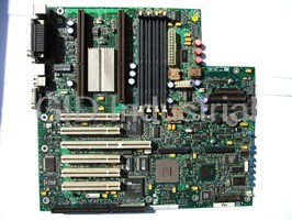

Intel LE80538 423 Processor - INTEL LE80538 423 Intel Pentium M processor
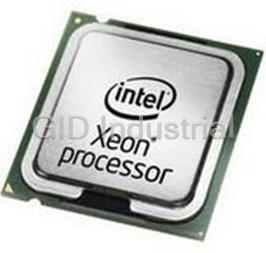
Intel LF80550KF0804M Xeon Processor. SL9HF Intel Xeon 7120N | 3.0GHz | Socket 604(mPGA604)
Intel LGA771-D36871-001-FRJ Heatsink. 2U | For Xeon 5000 Series Socket 771 Processors

Request a Quote

The quote request has been received
Close

Facing challenges or have inquiries? Feel free to contact us!
Call Us +1-469-283-2440
What they say about us
FANTASTIC RESOURCE
One of our top priorities is maintaining our business with precision, and we are constantly looking for affiliates that can help us achieve our goal. With the aid of GID Industrial, our obsolete product management has never been more efficient. They have been a great resource to our company, and have quickly become a go-to supplier on our list!
Bucher Emhart Glass
EXCELLENT SERVICE
With our strict fundamentals and high expectations, we were surprised when we came across GID Industrial and their competitive pricing. When we approached them with our issue, they were incredibly confident in being able to provide us with a seamless solution at the best price for us. GID Industrial quickly understood our needs and provided us with excellent service, as well as fully tested product to ensure what we received would be the right fit for our company.
Fuji
HARD TO FIND A BETTER PROVIDER
Our company provides services to aid in the manufacture of technological products, such as semiconductors and flat panel displays, and often searching for distributors of obsolete product we require can waste time and money. Finding GID Industrial proved to be a great asset to our company, with cost effective solutions and superior knowledge on all of their materials, it’d be hard to find a better provider of obsolete or hard to find products.
Applied Materials
CONSISTENTLY DELIVERS QUALITY SOLUTIONS
Over the years, the equipment used in our company becomes discontinued, but they’re still of great use to us and our customers. Once these products are no longer available through the manufacturer, finding a reliable, quick supplier is a necessity, and luckily for us, GID Industrial has provided the most trustworthy, quality solutions to our obsolete component needs.
Nidec Vamco
TERRIFIC RESOURCE
This company has been a terrific help to us (I work for Trican Well Service) in sourcing the Micron Ram Memory we needed for our Siemens computers. Great service! And great pricing! I know when the product is shipping and when it will arrive, all the way through the ordering process.
Trican Well Service
GO TO SOURCE
When I can't find an obsolete part, I first call GID and they'll come up with my parts every time. Great customer service and follow up as well. Scott emails me from time to time to touch base and see if we're having trouble finding something.....which is often with our 25 yr old equipment.
ConAgra Foods