

 Manufacturers
INTEL D910GLDW

Description
Intel D910GLDW CPU Board - 910 Chipset-Based Desktop Motherboard.
Part Number
D910GLDW
Price
Request Quote
Manufacturer
INTEL
Lead Time
Request Quote
Category
PRODUCTS - D
Specifications
Audio Codec
Realtek ALC860
Bus Clock
333 MHz, 400 MHz
Cache Memory
None
Chipset Type
Intel 910GL Express
Compatible Processors
Celeron D
Compliant Standards
High Definition Audio
Graphics Controller
Intel GMA 900
Max Bus Speed
533 MHz
Max Processors
Qty 1
Max Size
2 GB
Memory Allocation Technology
Dynamic Video Memory Technology 3.0
Processor
Intel Celeron
Processor Socket
LGA775 Socket
Product Type
Motherboard - Micro ATX
Speed PC2700, PC3200
Supported RAM
Technology
DDR SDRAM
Type
High Definition Audio
Features
- 533 MHz data bus speed
- Integrated audio
- Integrated Ethernet
- Integrated video
- Intel 910GL Express /Intel ICH6 chipset
- One (1) floppy controller
- One (1) IDE controllers
- Socket 775
- Supports 2 GB DDR
Datasheet

Extracted Text
®
Intel Desktop Board
D910GLDW
Technical Product Specification
October 2004
Order Number: C88966-002
®
The Intel Desktop Board D910GLDW may contain design defects or errors known as errata that may cause the product to deviate from published specifications. Current
characterized errata are documented in the Intel Desktop Board D910GLDW Specification Update.
Revision History
Revision Revision History Date
®
-001 First release of the Intel Desktop Board D910GLDW Technical Product September 2004
Specification.
®
-002 Second release of the Intel Desktop Board D910GLDW Technical Product October 2004
Specification.
®
This product specification applies to only standard Intel Desktop Board D910GLDW with BIOS
identifier WB91X10J.86A.
Changes to this specification will be published in the Intel Desktop Board D910GLDW
Specification Update before being incorporated into a revision of this document.
®
INFORMATION IN THIS DOCUMENT IS PROVIDED IN CONNECTION WITH INTEL PRODUCTS. NO LICENSE,
EXPRESS OR IMPLIED, BY ESTOPPEL OR OTHERWISE, TO ANY INTELLECTUAL PROPERTY RIGHTS IS GRANTED
BY THIS DOCUMENT. EXCEPT AS PROVIDED IN INTEL’S TERMS AND CONDITIONS OF SALE FOR SUCH
PRODUCTS, INTEL ASSUMES NO LIABILITY WHATSOEVER, AND INTEL DISCLAIMS ANY EXPRESS OR IMPLIED
WARRANTY, RELATING TO SALE AND/OR USE OF INTEL PRODUCTS INCLUDING LIABILITY OR WARRANTIES
RELATING TO FITNESS FOR A PARTICULAR PURPOSE, MERCHANTABILITY, OR INFRINGEMENT OF ANY PATENT,
COPYRIGHT OR OTHER INTELLECTUAL PROPERTY RIGHT. INTEL PRODUCTS ARE NOT INTENDED FOR USE IN
MEDICAL, LIFE SAVING, OR LIFE SUSTAINING APPLICATIONS.
Intel Corporation may have patents or pending patent applications, trademarks, copyrights, or other intellectual property
rights that relate to the presented subject matter. The furnishing of documents and other materials and information does not
provide any license, express or implied, by estoppel or otherwise, to any such patents, trademarks, copyrights, or other
intellectual property rights.
Intel may make changes to specifications and product descriptions at any time, without notice.
Designers must not rely on the absence or characteristics of any features or instructions marked “reserved” or “undefined.”
Intel reserves these for future definition and shall have no responsibility whatsoever for conflicts or incompatibilities arising
from future changes to them.
®
Intel desktop boards may contain design defects or errors known as errata, which may cause the product to deviate from
published specifications. Current characterized errata are available on request.
Contact your local Intel sales office or your distributor to obtain the latest specifications before placing your product order.
Copies of documents which have an ordering number and are referenced in this document, or other Intel literature, may be
obtained from:
Intel Corporation
P.O. Box 5937
Denver, CO 80217-9808
or call in North America 1-800-548-4725, Europe 44-0-1793-431-155, France 44-0-1793-421-777,
Germany 44-0-1793-421-333, other Countries 708-296-9333.
Intel, Pentium, and Celeron are registered trademarks of Intel Corporation or its subsidiaries in the United States and other
countries.
* Other names and brands may be claimed as the property of others.
Copyright © 2004, Intel Corporation. All rights reserved.
Preface
This Technical Product Specification (TPS) specifies the board layout, components, connectors,
®
power and environmental requirements, and the BIOS for the Intel Desktop Board D910GLDW.
It describes the standard product and available manufacturing options.
Intended Audience
The TPS is intended to provide detailed, technical information about the Desktop Board
D910GLDW and their components to the vendors, system integrators, and other engineers and
technicians who need this level of information. It is specifically not intended for general audiences.
What This Document Contains
Chapter Description
1 A description of the hardware used on the Desktop Board D910GLDW
2 A map of the resources of the Desktop Board
3 The features supported by the BIOS Setup program
4 A description of the BIOS error messages, beep codes, and POST codes
Typographical Conventions
This section contains information about the conventions used in this specification. Not all of these
symbols and abbreviations appear in all specifications of this type.
Notes, Cautions, and Warnings
NOTE
�
Notes call attention to important information.
INTEGRATOR’S NOTES
#
Integrator’s notes are used to call attention to information that may be useful to system integrators.
CAUTION
Cautions are included to help you avoid damaging hardware or losing data.
WARNING
Warnings indicate conditions, which if not observed, can cause personal injury.
iii
Intel Desktop Board D910GLDW Technical Product Specification
Other Common Notation
# Used after a signal name to identify an active-low signal (such as USBP0#)
(NxnX) When used in the description of a component, N indicates component type, xn are the relative
coordinates of its location on the Desktop Board D910GLDW, and X is the instance of the
particular part at that general location. For example, J5J1 is a connector, located at 5J. It is
the first connector in the 5J area.
GB Gigabyte (1,073,741,824 bytes)
GB/sec Gigabytes per second
KB Kilobyte (1024 bytes)
Kbit Kilobit (1024 bits)
kbits/sec 1000 bits per second
MB Megabyte (1,048,576 bytes)
MB/sec Megabytes per second
Mbit Megabit (1,048,576 bits)
Mbit/sec Megabits per second
xxh An address or data value ending with a lowercase h indicates a hexadecimal value.
x.x V Volts. Voltages are DC unless otherwise specified.
* This symbol is used to indicate third-party brands and names that are the property of their
respective owners.
iv
Contents
1 Product Description
1.1 PCI Bus Terminology Change........................................................................................9
1.2 Overview ......................................................................................................................10
1.2.1 Feature Summary..........................................................................................10
1.2.2 Manufacturing Options ..................................................................................11
1.2.3 Board Layout .................................................................................................12
1.2.4 Block Diagram ...............................................................................................14
1.3 Online Support .............................................................................................................15
1.4 Processor.....................................................................................................................15
1.5 System Memory ...........................................................................................................15
1.5.1 Memory Configurations .................................................................................17
®
1.6 Intel 910GL Chipset ...................................................................................................19
1.6.1 Intel 910GL Graphics Controller....................................................................19
1.6.2 USB ...............................................................................................................20
1.6.3 IDE Support...................................................................................................20
1.6.4 Real-Time Clock, CMOS SRAM, and Battery................................................22
1.7 PCI Express Connector................................................................................................22
1.8 I/O Controller................................................................................................................23
1.8.1 Serial Port......................................................................................................23
1.8.2 Parallel Port...................................................................................................23
1.8.3 Diskette Drive Controller................................................................................23
1.8.4 Keyboard and Mouse Interface .....................................................................23
1.9 Audio Subsystem .........................................................................................................24
1.9.1 Audio Subsystem Software ...........................................................................24
1.9.2 Audio Connectors..........................................................................................24
®
1.9.3 Intel High Definition Audio Subsystem ........................................................25
1.10 LAN Subsystem (Optional)...........................................................................................26
®
1.10.1 Intel 82562EZ Physical Layer Interface Device...........................................26
1.10.2 Alert Standard Format (ASF) Support ...........................................................27
1.10.3 LAN Subsystem Software..............................................................................27
1.11 Hardware Management Subsystem.............................................................................28
1.11.1 Hardware Monitoring and Fan Control ASIC .................................................28
1.11.2 Thermal Monitoring........................................................................................29
1.11.3 Fan Monitoring...............................................................................................30
®
1.11.4 Fan Speed Control (Intel Precision Cooling Technology) ...........................30
1.11.5 Chassis Intrusion and Detection....................................................................30
1.12 Power Management .....................................................................................................30
1.12.1 ACPI ..............................................................................................................31
1.12.2 Hardware Support .........................................................................................33
2 Technical Reference
2.1 Introduction ..................................................................................................................37
2.2 Memory Map ................................................................................................................37
2.3 Fixed I/O Map...............................................................................................................38
2.4 DMA Channels.............................................................................................................39
v
Intel Desktop Board D910GLDW Technical Product Specification
2.5 PCI Configuration Space Map......................................................................................39
2.6 Interrupts......................................................................................................................40
2.7 PCI Conventional Interrupt Routing Map .....................................................................41
2.8 Connectors...................................................................................................................42
2.8.1 Back Panel Connectors.................................................................................42
2.8.2 Component-side Connectors.........................................................................44
2.9 Jumper Block ...............................................................................................................52
2.10 Mechanical Considerations..........................................................................................53
2.10.1 Form Factor...................................................................................................53
2.10.2 I/O Shield.......................................................................................................54
2.11 Electrical Considerations..............................................................................................55
2.11.1 DC Loading....................................................................................................55
2.11.2 Add-in Board Considerations.........................................................................55
2.11.3 Fan Connector Current Capability.................................................................55
2.11.4 Power Supply Considerations .......................................................................56
2.12 Thermal Considerations...............................................................................................57
2.13 Reliability......................................................................................................................59
2.14 Environmental ..............................................................................................................60
2.15 Regulatory Compliance................................................................................................61
2.15.1 Safety Regulations ........................................................................................61
2.15.2 EMC Regulations...........................................................................................61
2.15.3 European Union Declaration of Conformity Statement..................................62
2.15.4 Product Ecology Statements .........................................................................63
2.15.5 Product Certification Markings (Board Level) ................................................64
3 Overview of BIOS Features
3.1 Introduction ..................................................................................................................65
3.2 BIOS Flash Memory Organization ...............................................................................66
3.3 Resource Configuration ...............................................................................................66
3.3.1 PCI Autoconfiguration....................................................................................66
3.3.2 PCI IDE Support ............................................................................................66
3.4 System Management BIOS (SMBIOS) ........................................................................67
3.5 Legacy USB Support....................................................................................................67
3.6 BIOS Updates ..............................................................................................................68
3.6.1 Language Support.........................................................................................68
3.6.2 Custom Splash Screen..................................................................................68
3.7 Boot Options ................................................................................................................69
3.7.1 CD-ROM Boot ...............................................................................................69
3.7.2 Network Boot.................................................................................................69
3.7.3 Booting Without Attached Devices ................................................................69
3.7.4 Changing the Default Boot Device During POST ..........................................69
®
3.8 Fast Booting Systems with Intel Rapid BIOS Boot ....................................................70
3.8.1 Peripheral Selection and Configuration.........................................................70
3.8.2 Intel Rapid BIOS Boot ...................................................................................70
3.9 BIOS Security Features ...............................................................................................71
vi
Contents
4 Error Messages and Beep Codes
4.1 BIOS Error Messages ..................................................................................................73
4.2 Port 80h POST Codes .................................................................................................75
4.3 Bus Initialization Checkpoints ......................................................................................79
4.4 Speaker .......................................................................................................................80
4.5 BIOS Beep Codes........................................................................................................80
Figures
1. Board Components......................................................................................................12
2. Block Diagram..............................................................................................................14
3. Memory Channel Configuration ...................................................................................17
4. Dual Channel (Interleaved) Mode Configuration with Two DIMMs ..............................18
5. Single Channel (Asymmetric) Mode Configuration with One DIMM.............................18
6. Front/Back Panel Audio Connector Options for High Definition Audio Subsystem......25
7. High Definition Audio Subsystem Block Diagram ........................................................25
8. LAN Connector LED Locations ....................................................................................26
9. Thermal Monitoring......................................................................................................29
10. Location of the Standby Power Indicator LED .............................................................36
11. Back Panel Connectors................................................................................................42
12. Component-side Connectors.......................................................................................44
13. Connection Diagram for Front Panel Connector ..........................................................49
14. Connection Diagram for Front Panel USB Connectors................................................50
15. Connection Diagram for IEEE 1394a Connector .........................................................51
16. Location of the Jumper Block.......................................................................................52
17. Board Dimensions........................................................................................................53
18. I/O Shield Dimensions..................................................................................................54
19. Processor Heatsink Airflow ..........................................................................................57
20. Localized High Temperature Zones.............................................................................58
Tables
1. Feature Summary ........................................................................................................10
2. Manufacturing Options.................................................................................................11
3. Board Components Shown in Figure 1 ........................................................................13
4. Supported Memory Configurations ..............................................................................16
5. LAN Connector LED States .........................................................................................26
6. Effects of Pressing the Power Switch ..........................................................................31
7. Power States and Targeted System Power .................................................................32
8. Wake-up Devices and Events......................................................................................33
9. System Memory Map ...................................................................................................37
10. I/O Map .......................................................................................................................38
11. DMA Channels.............................................................................................................39
12. PCI Configuration Space Map......................................................................................39
13. Interrupts......................................................................................................................40
14. PCI Interrupt Routing Map ...........................................................................................41
15. Back Panel Connectors Shown in Figure 11................................................................43
16. Component-side Connectors Shown in Figure 12 .......................................................45
17. Front Panel Audio Connector.......................................................................................46
vii
Intel Desktop Board D910GLDW Technical Product Specification
18. Front Chassis Fan and Rear Chassis Fan Connectors................................................46
19. Processor Fan Connector ............................................................................................46
20. Chassis Intrusion Connector........................................................................................46
21. Serial ATA Connectors.................................................................................................46
22. Main Power Connector.................................................................................................47
23. ATX12V Power Connector ...........................................................................................47
24. Auxiliary Front Panel Power/Sleep LED Connector .....................................................48
25. Front Panel Connector.................................................................................................48
26. States for a One-Color Power LED ..............................................................................49
27. States for a Two-Color Power LED ..............................................................................49
28. BIOS Setup Configuration Jumper Settings.................................................................52
29. DC Loading Characteristics .........................................................................................55
30. Fan Connector Current Capability................................................................................55
31. Thermal Considerations for Components ....................................................................59
32. Environmental Specifications.......................................................................................60
33. Safety Regulations.......................................................................................................61
34. EMC Regulations .........................................................................................................61
35. Product Certification Markings .....................................................................................64
36. BIOS Setup Program Menu Bar...................................................................................66
37. BIOS Setup Program Function Keys............................................................................66
38. Boot Device Menu Options ..........................................................................................69
39. Supervisor and User Password Functions...................................................................71
40. BIOS Error Messages ..................................................................................................73
41. Uncompressed INIT Code Checkpoints.......................................................................75
42. Boot Block Recovery Code Checkpoints .....................................................................75
43. Runtime Code Uncompressed in F000 Shadow RAM .................................................76
44. Bus Initialization Checkpoints ......................................................................................79
45. Upper Nibble High Byte Functions...............................................................................79
46. Lower Nibble High Byte Functions...............................................................................80
47. Beep Codes .................................................................................................................80
viii
1 Product Description
What This Chapter Contains
1.1 PCI Bus Terminology Change........................................................................................9
1.2 Overview ......................................................................................................................10
1.3 Online Support .............................................................................................................15
1.4 Processor.....................................................................................................................15
1.5 System Memory ...........................................................................................................15
®
1.6 Intel 910GL Chipset ...................................................................................................19
1.7 PCI Express Connector................................................................................................22
1.8 I/O Controller................................................................................................................23
1.9 Audio Subsystem .........................................................................................................24
1.10 LAN Subsystem (Optional)...........................................................................................26
1.11 Hardware Management Subsystem.............................................................................28
1.12 Power Management .....................................................................................................30
1.1 PCI Bus Terminology Change
®
Previous generations of Intel Desktop Boards used an add-in card connector referred to as PCI.
This generation of Intel Desktop Boards adds a new technology for add-in cards: PCI Express*.
The 32-bit parallel bus previously referred to as PCI is now called PCI Conventional.
9
Intel Desktop Board D910GLDW Technical Product Specification
1.2 Overview
1.2.1 Feature Summary
Table 1 summarizes the major features of the Desktop Board D910GLDW.
Table 1. Feature Summary
Form Factor microATX Form Factor (9.60 inches by 9.60 inches [243.84 millimeters by
243.84 millimeters])
® ®
Processor Support for an Intel Celeron processor in an LGA775 socket
Memory
• Two DDR SDRAM Dual Inline Memory Module (DIMM) sockets
• Support for DDR 400 MHz and DDR 333 MHz DIMMs
• Support for up to 2 GB of system memory
Chipset ®
Intel 910GL Chipset, consisting of:
®
• Intel 82910GL Graphics Memory Controller Hub (GMCH)
®
• Intel 82801FB I/O Controller Hub (ICH6)
• 4 Mbit Firmware Hub (FWH)
®
Video Intel GMA900 onboard graphics subsystem
®
Audio Intel High Definition Audio subsystem using the Realtek ALC860 audio codec
I/O Control LPC Bus I/O controller
USB Support for USB 2.0 devices
Peripheral • Eight USB ports
Interfaces
• One serial port
• One parallel port
• Four Serial ATA interfaces
• One Parallel ATA IDE interface with UDMA 33, ATA-66/100 support
• One diskette drive interface
• PS/2* keyboard and mouse ports
BIOS • 4 Mbit FWH
®
• Intel Rapid BIOS Boot
• Support for Advanced Configuration and Power Interface (ACPI), Plug and Play,
and SMBIOS
Instantly Available • Support for PCI Local Bus Specification Revision 2.2
PC Technology
• Support for PCI Express Revision 1.0a
• Suspend to RAM support
• Wake on PCI, RS-232, front panel, PS/2 devices, and USB ports
continued
10
Product Description
Table 1. Feature Summary (continued)
Expansion • Two PCI Conventional bus add-in card connectors (SMBus routed to PCI
Conventional bus connector 2)
Capabilities
• One PCI Express x1 bus add-in card connector
Hardware Monitor • Hardware monitoring and fan control ASIC
Subsystem
• Voltage sense to detect out of range power supply voltages
• Thermal sense to detect out of range thermal values
• Three fan connectors
• Three fan sense inputs used to monitor fan activity
• Fan speed control
1.2.2 Manufacturing Options
Table 2 describes the manufacturing options on the Desktop Board D910GLDW. Not every
manufacturing option is available in all marketing channels. Please contact your Intel
representative to determine which manufacturing options are available to you.
Table 2. Manufacturing Options
IEEE-1394a IEEE-1394a controller and two IEEE-1394a connectors
Interface
®
LAN Support 10/100 Mbits/sec LAN subsystem using the Intel 82562EZ Platform LAN Connect
(PLC) device
For information about Refer to
Available configurations for the Desktop Board D910GLDW Section 1.3, page 15
11
Intel Desktop Board D910GLDW Technical Product Specification
1.2.3 Board Layout
Figure 1 shows the location of the major components on the Desktop Board D910GLDW.
ABC D E
F
DD
CC
G
BB
H
AA
I
Z
J
K
Y
L
W U S
R
X V T Q P O N M
OM17306
Figure 1. Board Components
Table 3 lists the components identified in Figure 1.
12
Product Description
Table 3. Board Components Shown in Figure 1
Item/Callout
from Figure 1 Description
A Realtek ALC860 audio codec
B Front panel audio connector (Yellow)
C
PCI Conventional bus add-in card connectors
D
Rear chassis fan connector
E
Back panel connectors
F +12V power connector (ATX12V)
G LGA775 processor socket
H Hardware monitoring and fan control ASIC
I
Processor fan connector
J
Intel 82910GL GMCH
K DIMM Channel A socket
L DIMM Channel B socket
M I/O controller
N
Power connector
O
Diskette drive connector
P
Parallel ATE IDE connector
Q Battery
R Chassis intrusion connector
S BIOS Setup configuration jumper block
T
4 Mbit Firmware Hub (FWH)
U
Front chassis fan connector
V Serial ATA connectors
W Auxiliary front panel power LED connector
X Front panel connector
Y Front panel USB connectors
Z
Intel 82801FB I/O Controller Hub (ICH6)
AA
Front panel IEEE-1394a connectors (optional)
BB IEEE-1394a controller (optional)
CC Speaker
DD PCI Express x1 bus add-in card connector
13
Intel Desktop Board D910GLDW Technical Product Specification
1.2.4 Block Diagram
Figure 2 is a block diagram of the major functional areas of the board.
Back Panel/Front Panel
USB
USB Ports
PCI Express
PCI Express x1 Slot 1
x1 Interface
Serial Ports
LPC Bus
Parallel Port
Parallel ATA Parallel ATA
I/O
PS/2 Mouse
IDE Connector IDE Interface
Controller
PS/2 Keyboard
LGA775 System Bus Diskette Drive
Processor Socket (533 MHz) Connector
LPC Bus
Intel 82910GL
Intel 82801FB 4 Mbit
Graphics and
I/O Controller Hub Firmware Hub
Memory Controller
(ICH6) (FWH)
Hub (GMCH)
Intel 910GL Chipset
VGA
Display Interface
Port
Dual-Channel
Memory Bus
Channel A
SMBus
DIMM
10/100 LAN
LAN PLC Connector
Channel B
(Optional) (Optional)
DIMM
IEEE-1394a Connectors
Serial ATA Serial ATA IDE
PCI Bus
(Optional)
IDE Interface Connectors (4)
PCI Bus
Mic In/Retasking Jack B
PCI Slot 1
Line In/Retasking Jack C
PCI Slot 2
SMBus
Audio
Line Out/Retasking Jack D
Codec
Retasking Jack E [Port 1]
Hardware Monitoring Retasking Jack F [Port 2]
and Fan Control ASIC
= connector or socket
OM17307
Figure 2. Block Diagram
14
DMI Interconnect
High Definition Audio Link
LAN Connect
Interface
Product Description
1.3 Online Support
To find information about… Visit this World Wide Web site:
Intel Desktop Board D910GLDW under http://www.intel.com/design/motherbd
“Desktop Board Products” or “Desktop
Board Support” http://support.intel.com/support/motherboards/desktop
Available configurations for the Desktop http://developer.intel.com/design/motherbd/dw/dw_available.htm
Board D910GLDW
Processor data sheets http://www.intel.com/design/litcentr
ICH6 addressing http://developer.intel.com/design/chipsets/datashts
Custom splash screens http://intel.com/design/motherbd/gen_indx.htm
Audio software and utilities http://www.intel.com/design/motherbd
LAN software and drivers http://www.intel.com/design/motherbd
1.4 Processor
The board is designed to support an Intel Celeron processor in an LGA775 processor socket with a
533 MHz system bus. See the Intel web site listed below for the most up-to-date list of supported
processors.
For information about… Refer to:
Supported processors for the D910GLDW board http://www.intel.com/design/motherbd/dw/dw_proc.htm
CAUTION
Use only the processors listed on web site above. Use of unsupported processors can damage the
board, the processor, and the power supply.
INTEGRATOR’S NOTE
#
Use only ATX12V-compliant power supplies.
For information about Refer to
Power supply connectors Section 2.8.2.1, page 47
1.5 System Memory
The board has two DIMM sockets and supports the following memory features:
• 2.5 V (only) DDR SDRAM DIMMs with gold-plated contacts
• Unbuffered, single-sided or double-sided DIMMs with the following restriction:
Double-sided DIMMS with x16 organization are not supported.
• 2 GB maximum total system memory
• Minimum total system memory: 128 MB
• Non-ECC DIMMs
• Serial Presence Detect
• DDR 400 MHz and DDR 333 MHz SDRAM DIMMs
15
Intel Desktop Board D910GLDW Technical Product Specification
NOTE
�
To be fully compliant with all applicable DDR SDRAM memory specifications, the board should be
populated with DIMMs that support the Serial Presence Detect (SPD) data structure. This allows
the BIOS to read the SPD data and program the chipset to accurately configure memory settings
for optimum performance. If non-SPD memory is installed, the BIOS will attempt to correctly
configure the memory settings, but performance and reliability may be impacted or the DIMMs
may not function under the determined frequency.
Table 4 lists the supported DIMM configurations.
Table 4. Supported Memory Configurations
DIMM SDRAM SDRAM Organization Number of SDRAM
Capacity Configuration Density Front-side/Back-side Devices
128 MB SS 256 Mbit 16 M x 16/empty 4
256 MB SS 256 Mbit 32 M x 8/empty 8
256 MB SS 512 Mbit 32 M x 16/empty 4
512 MB DS 256 Mbit 32 M x 8/32 M x 8 16
512 MB SS 512 Mbit 64 M x 8/empty 8
512 MB SS 1 Gbit 64 M x 16/empty 4
1024 MB DS 512 Mbit 64 M x 8/64 M x 8 16
1024 MB SS 1 Gbit 128 M x 8/empty 8
2048 MB DS 1 Gbit 128 M x 8/128 M x 8 16
Note: In the second column, “DS” refers to double-sided memory modules (containing two rows of SDRAM) and “SS” refers
to single-sided memory modules (containing one row of SDRAM).
16
Product Description
1.5.1 Memory Configurations
The Intel 82910GL GMCH supports two types of memory organization:
• Dual channel (Interleaved) mode. This mode offers the highest throughput for real world
applications. Dual channel mode is enabled when the installed memory capacities of both
DIMM channels are equal. Technology and device width can vary from one channel to the
other but the installed memory capacity for each channel must be equal. If different speed
DIMMs are used between channels, the slowest memory timing will be used.
• Single channel (Asymmetric) mode. This mode is equivalent to single channel bandwidth
operation for real world applications. This mode is used when only a single DIMM is installed
or the memory capacities are unequal. Technology and device width can vary from one
channel to the other. If different speed DIMMs are used between channels, the slowest
memory timing will be used.
Figure 3 illustrates the memory channel and DIMM configuration.
Channel A, DIMM 0
Channel B, DIMM 0
OM17308
Figure 3. Memory Channel Configuration
17
Intel Desktop Board D910GLDW Technical Product Specification
1.5.1.1 Dual Channel (Interleaved) Mode Configuration
Figure 4 shows a dual channel configuration using two DIMMs. In this example, the DIMM
sockets of both channels are populated with identical DIMMs.
1 GB Channel A, DIMM 0
1 GB
Channel B, DIMM 0
OM17309
Figure 4. Dual Channel (Interleaved) Mode Configuration with Two DIMMs
1.5.1.2 Single Channel (Asymmetric) Mode Configuration
NOTE
�
Dual channel (Interleaved) mode configurations provide the highest memory throughput.
Figure 5 shows a single channel configuration using one DIMM. In this example, only the Channel
A DIMM socket is populated. Channel B is not populated.
256 MB Channel A, DIMM 0
Channel B, DIMM 0
OM17310
Figure 5. Single Channel (Asymmetric) Mode Configuration with One DIMM
18
Product Description
®
1.6 Intel 910GL Chipset
The Intel 910GL chipset consists of the following devices:
• Intel 82910GL Graphics Memory Controller Hub (GMCH) with Direct Media Interface (DMI)
interconnect
• Intel 82801FB I/O Controller Hub (ICH6) with DMI interconnect
• Firmware Hub (FWH)
The GMCH is a centralized controller for the system bus, the memory bus, the PCI Express bus,
and the DMI interconnect. The ICH6 is a centralized controller for the board’s I/O paths. The
FWH provides the nonvolatile storage of the BIOS.
For information about Refer to
The Intel 910GL chipset http://developer.intel.com/
Resources used by the chipset Chapter 2
1.6.1 Intel 910GL Graphics Controller
The Intel GMA900 graphics controller features the following:
• Integrated graphics controller
⎯ 32 bpp (Bits Per Pixel) graphics engine
⎯ 333 MHz core frequency
⎯ 256-bit 2-D engine
⎯ 32-bit 3-D engine
⎯ Motion video acceleration
⎯ Pixel Shader 2.0
⎯ 4-pixel pipes
⎯ DirectX 9.0 Hardware Acceleration
⎯ Software Vertex Shader
• Up to 2048 x 1536 at 75 Hz refresh
• High performance 3-D setup and render engine
• High quality/performance texture engine
• Display
⎯ Integrated 24-bit 400 MHz RAMDAC
⎯ DDC2B compliant interface
• Video hardware motion compensation for software MPEG2 decode
• Dynamic Video Memory Technology (DVMT) support up to 224 MB
®
• Intel Zoom Utility
For information about Refer to
DVMT Section 0, page 20
Obtaining graphics software and utilities Section 1.3, page 15
19
Intel Desktop Board D910GLDW Technical Product Specification
1.6.1.1 Dynamic Video Memory Technology (DVMT)
DVMT enables enhanced graphics and memory performance through Direct AGP, and highly
efficient memory utilization. DVMT ensures the most efficient use of available system memory for
maximum 2-D/3-D graphics performance. Up to 224 MB of system memory can be allocated to
DVMT on systems that have 512 MB or more of total system memory installed. Up to 128 MB can
be allocated to DVMT on systems that have 256 MB but less than 512 MB of total installed system
memory. Up to 64 MB can be allocated to DVMT when less than 256 MB of system memory is
installed. DVMT returns system memory back to the operating system when the additional system
memory is no longer required by the graphics subsystem.
DVMT will always use a minimal fixed portion of system physical memory (as set in the BIOS
Setup program) for compatibility with legacy applications. An example of this would be when
using VGA graphics under DOS. Once loaded, the operating system and graphics drivers allocate
additional system memory to the graphics buffer as needed for performing graphics functions.
NOTE
�
The use of DVMT requires operating system driver support.
1.6.2 USB
The board supports up to eight USB 2.0 ports, supports UHCI and EHCI, and uses UHCI- and
EHCI-compatible drivers.
The ICH6 provides the USB controller for all ports. The port arrangement is as follows:
• Four ports are implemented with dual stacked back panel connectors adjacent to the audio
connectors
• Four ports are routed to two separate front panel USB connectors
NOTE
�
Computer systems that have an unshielded cable attached to a USB port may not meet FCC
Class B requirements, even if no device is attached to the cable. Use shielded cable that meets the
requirements for full-speed devices.
For information about Refer to
The location of the USB connectors on the back panel Figure 11, page 42
The location of the front panel USB connectors Figure 12, page 44
1.6.3 IDE Support
The board provides five IDE interface connectors:
• One parallel ATA IDE connector that supports two devices
• Four serial ATA IDE connectors that support one device per connector
20
Product Description
1.6.3.1 Parallel ATE IDE Interface
The ICH6’s Parallel ATA IDE controller has one bus-mastering Parallel ATA IDE interface. The
Parallel ATA IDE interface supports the following modes:
• Programmed I/O (PIO): processor controls data transfer.
• 8237-style DMA: DMA offloads the processor, supporting transfer rates of up to 16 MB/sec.
• Ultra DMA: DMA protocol on IDE bus supporting host and target throttling and transfer rates
of up to 33 MB/sec.
• ATA-66: DMA protocol on IDE bus supporting host and target throttling and transfer rates of
up to 66 MB/sec. ATA-66 protocol is similar to Ultra DMA and is device driver compatible.
• ATA-100: DMA protocol on IDE bus allows host and target throttling. The ICH6’s ATA-100
logic can achieve read transfer rates up to 100 MB/sec and write transfer rates up to 88 MB/sec.
� NOTE
ATA-66 and ATA-100 are faster timings and require a specialized cable to reduce reflections,
noise, and inductive coupling.
The Parallel ATA IDE interface also supports ATAPI devices (such as CD-ROM drives) and ATA
devices using the transfer modes.
The BIOS supports Logical Block Addressing (LBA) and Extended Cylinder Head Sector (ECHS)
translation modes. The drive reports the transfer rate and translation mode to the BIOS.
The board supports Laser Servo (LS-120) diskette technology through the Parallel ATA IDE
interfaces. An LS-120 drive can be configured as a boot device by setting the BIOS Setup
program’s Boot menu to one of the following:
• ARMD-FDD (ATAPI removable media device – floppy disk drive)
• ARMD-HDD (ATAPI removable media device – hard disk drive)
For information about Refer to
The location of the Parallel ATA IDE connector Figure 12, page 44
1.6.3.2 Serial ATA Interfaces
The ICH6’s Serial ATA controller offers four independent Serial ATA ports with a theoretical
maximum transfer rate of 150 MB/s per port. One device can be installed on each port for a
maximum of four Serial ATA devices. A point-to-point interface is used for host to device
connections, unlike Parallel ATA IDE which supports a master/slave configuration and two devices
per channel.
For compatibility, the underlying Serial ATA functionality is transparent to the operating system.
The Serial ATA controller can operate in both legacy and native modes. In legacy mode, standard
IDE I/O and IRQ resources are assigned (IRQ 14 and 15). In Native mode, standard PCI
Conventional bus resource steering is used. Native mode is the preferred mode for configurations
using the Windows* XP and Windows 2000 operating systems.
21
Intel Desktop Board D910GLDW Technical Product Specification
NOTE
�
Many Serial ATA drives use new low-voltage power connectors and require adaptors or power
supplies equipped with low-voltage power connectors.
For more information, see: http://www.serialata.org/
For information about Refer to
The location of the Serial ATA IDE connectors Figure 12, page 44
1.6.4 Real-Time Clock, CMOS SRAM, and Battery
A coin-cell battery (CR2032) powers the real-time clock and CMOS memory. When the computer
is not plugged into a wall socket, the battery has an estimated life of three years. When the
computer is plugged in, the standby current from the power supply extends the life of the battery.
The clock is accurate to ± 13 minutes/year at 25 ºC with 3.3 VSB applied.
� NOTE
If the battery and AC power fail, custom defaults, if previously saved, will be loaded into CMOS
RAM at power-on.
1.7 PCI Express Connector
The board provides one PCI Express x1 connector. The x1 interface supports simultaneous transfer
speeds up to 500 MBytes/sec.
The PCI Express interface supports the PCI Conventional bus configuration mechanism so that the
underlying PCI Express architecture is compatible with PCI Conventional compliant operating
systems. Additional features of the PCI Express interface includes the following:
• Support for the PCI Express enhanced configuration mechanism
• Automatic discovery, link training, and initialization
• Support for Active State Power Management (ASPM)
• SMBus 2.0 support
• Wake# signal supporting wake events from ACPI S1, S3, S4, or S5
• Software compatible with the PCI Power Management Event (PME) mechanism defined in the
PCI Power Management Specification Rev. 1.1
22
Product Description
1.8 I/O Controller
The I/O controller provides the following features:
• One serial port
• One parallel port with Extended Capabilities Port (ECP) and Enhanced Parallel Port
(EPP) support
• Serial IRQ interface compatible with serialized IRQ support for PCI Conventional bus systems
• PS/2-style mouse and keyboard interfaces
• Interface for one 1.44 MB or 2.88 MB diskette drive
• Intelligent power management, including a programmable wake-up event interface
• PCI Conventional bus power management support
The BIOS Setup program provides configuration options for the I/O controller.
1.8.1 Serial Port
The board supports one serial port connector, Serial port A, located on the back panel. The serial
port supports data transfers at speeds up to 115.2 kbits/sec with BIOS support.
For information about Refer to
The location of the serial port A connector Figure 11, page 42
1.8.2 Parallel Port
The 25-pin D-Sub parallel port connector is located on the back panel. Use the BIOS Setup
program to set the parallel port mode.
For information about Refer to
The location of the parallel port connector Figure 11, page 42
1.8.3 Diskette Drive Controller
The I/O controller supports one diskette drive. Use the BIOS Setup program to configure the
diskette drive interface.
For information about Refer to
The location of the diskette drive connector Figure 12, page 44
1.8.4 Keyboard and Mouse Interface
PS/2 keyboard and mouse connectors are located on the back panel.
NOTE
�
The keyboard is supported in the bottom PS/2 connector and the mouse is supported in the top PS/2
connector. Power to the computer should be turned off before a keyboard or mouse is connected or
disconnected.
For information about Refer to
The location of the keyboard and mouse connectors Figure 11, page 42
23
Intel Desktop Board D910GLDW Technical Product Specification
1.9 Audio Subsystem
The board supports the Intel High Definition audio subsystem based on the Realtek ALC860 codec.
The audio subsystem supports the following features:
• Advanced jack sense (front and rear panel) that enables the audio codec to recognize the device
that is connected to an audio port. All jacks are capable of retasking according to user’s
definition, or can be automatically switched depending on the recognized device type.
• Stereo input and output for all jacks.
• A signal-to-noise (S/N) ratio of 90 dB.
INTEGRATOR’S NOTE
#
For the front panel jack sensing and automatic retasking feature to function, a front panel daughter
card that is designed for Intel High Definition Audio must be used. Otherwise, an AC ’97 style
audio front panel connector will be assumed and the Line Out and Mic In functions will be
permanent.
1.9.1 Audio Subsystem Software
Audio software and drivers are available from Intel’s World Wide Web site.
For information about Refer to
Obtaining audio software and drivers Section 1.3, page 15
1.9.2 Audio Connectors
The board contains audio connectors on both the back panel and the component side of the board.
The front panel audio connector (located on the component-side of the board) is a 2 x 5-pin
connector that provides mic in and line out signals for front panel audio connectors.
For information about Refer to
The location of the front panel audio connector. Figure 12, page 44
The signal names of the front panel audio connector Table 17, page 46
24
Product Description
®
1.9.3 Intel High Definition Audio Subsystem
The Intel High Definition Audio subsystem includes the following:
• Intel 82801FB I/O Controller Hub (ICH6)
• Realtek ALC860 audio codec
• Microphone input that supports a single dynamic, condenser, or electret microphone
The front and back audio connectors are configurable through the audio device drivers. The
available configurable audio ports are shown in Figure 6.
Front Panel Back Panel
Audio Connectors Audio Connectors
Mic In/
Line Out/
Retasking Jack E Line In/
Retasking Jack F
[Port 1] Retasking Jack C
[Port 2]
Line Out/
Retasking Jack D
Mic In/
Retasking Jack B
OM16989
Figure 6. Front/Back Panel Audio Connector Options for High Definition Audio Subsystem
Figure 7 is a block diagram of the High Definition audio subsystem.
Mic In/Retasking Jack B
Line In/Retasking Jack C
82801FB
Intel
ALC860
I/O Controller
Line Out/Retasking Jack D
High Definition
Audio Codec
Hub
Audio Link
Front Panel Mic In/Retasking Jack E [Port 1]
(ICH6)
Front Panel Line Out/Retasking Jack F [Port 2]
OM17311
Figure 7. High Definition Audio Subsystem Block Diagram
For information about Refer to
The back panel audio connectors Figure 11, page 42
25
Intel Desktop Board D910GLDW Technical Product Specification
1.10 LAN Subsystem (Optional)
The 10/100 Mbits/sec LAN subsystem consists of the following:
• The Intel 82801FB ICH6
• An Intel 82562EZ Platform LAN Connect (PLC) device for 10/100 Mbits/sec Ethernet LAN
connectivity
• An RJ-45 LAN connector with integrated status LEDs
Additional features of the LAN subsystem include:
• CSMA/CD protocol engine
• LAN Connect Interface (LCI) between the 82562EZ and the ICH6
• PCI Conventional bus power management
⎯ Supports ACPI technology
⎯ Supports LAN wake capabilities
®
1.10.1 Intel 82562EZ Physical Layer Interface Device
The Intel 82562EZ provides the following functions:
• Basic 10/100 Ethernet LAN connectivity
• Full device driver compatibility
• Programmable transit threshold
• Configuration EEPROM that contains the MAC address
1.10.1.1 RJ-45 LAN Connector with Integrated LEDs
Two LEDs are built into the RJ-45 LAN connector (shown in Figure 8 below).
Green LED Yellow LED
OM15076
Figure 8. LAN Connector LED Locations
Table 5 describes the LED states when the board is powered up and the 10/100 Mbits/sec LAN
subsystem is operating.
Table 5. LAN Connector LED States
LED Color LED State Condition
Green Off LAN link is not established.
On LAN link is established.
Blinking LAN activity is occurring.
Yellow Off 10 Mbits/sec data rate is selected
On 100 Mbits/sec data rate is selected
26
Product Description
1.10.2 Alert Standard Format (ASF) Support
The boards provide the following ASF support for PCI Express x1 bus add-in LAN cards and PCI
Conventional bus add-in LAN cards installed in PCI Conventional bus slot 2:
• Monitoring of system firmware progress events, including:
⎯ BIOS present
⎯ Primary processor initialization
⎯ Memory initialization
⎯ Video initialization
⎯ PCI resource configuration
⎯ Hard-disk initialization
⎯ User authentication
⎯ Starting operating system boot process
• Monitoring of system firmware error events, including:
⎯ Memory missing
⎯ Memory failure
⎯ No video device
⎯ Keyboard failure
⎯ Hard-disk failure
⎯ No boot media
• Boot options to boot from different types of boot devices
• Reset, shutdown, power cycle, and power up options
1.10.3 LAN Subsystem Software
LAN software and drivers are available from Intel’s World Wide Web site.
For information about Refer to
Obtaining LAN software and drivers Section 1.3, page 15
27
Intel Desktop Board D910GLDW Technical Product Specification
1.11 Hardware Management Subsystem
The hardware management features enable the board to be compatible with the Wired for
Management (WfM) specification. The Desktop Board has several hardware management features,
including the following:
• Fan monitoring and control (through the hardware monitoring and fan control ASIC)
• Thermal and voltage monitoring
• Chassis intrusion detection
1.11.1 Hardware Monitoring and Fan Control ASIC
The features of the hardware monitoring and fan control ASIC include:
• Internal ambient temperature sensor
• Two remote thermal diode sensors for direct monitoring of processor temperature and ambient
temperature sensing
• Power supply monitoring of five voltages (+5 V, +12 V, +3.3 VSB, +1.5 V, and +VCCP) to
detect levels above or below acceptable values
• Thermally monitored closed-loop fan control, for all three fans, that can adjust the fan speed or
switch the fans on or off as needed
• SMBus interface
For information about Refer to
The location of the fan connectors and sensors for thermal monitoring Figure 9, page 29
28
Product Description
1.11.2 Thermal Monitoring
Figure 9 shows the location of the sensors and fan connectors.
3
1
A
B
C
4
D
1
1
3
F E
OM17312
Item Description
A Thermal diode, located on processor die
B
Remote ambient temperature sensor
C
Ambient temperature sensor, internal to hardware monitoring and fan control ASIC
D
Processor fan
E
Rear chassis fan
F
Front chassis fan
Figure 9. Thermal Monitoring
29
Intel Desktop Board D910GLDW Technical Product Specification
1.11.3 Fan Monitoring
®
Fan monitoring can be implemented using Intel Desktop Utilities, LANDesk* software, or third-
party software. The level of monitoring and control is dependent on the hardware monitoring ASIC
used with the Desktop Board.
For information about Refer to
The functions of the fan connectors Section 1.12.2.2, page 34
®
1.11.4 Fan Speed Control (Intel Precision Cooling Technology)
®
Intel Precision Cooling Technology automatically adjusts the processor fan speed based on the
processor thermal diode temperature and adjusts the chassis fan speeds depending on the system
temperature. System fan noise may be reduced by operating controlled chassis and processor fans
at the minimum necessary speeds.
The processor and chassis fan speed control features can be disabled independently through the
desktop board BIOS. Disabling the processor fan speed control will result in the fan operating at
full speed if it is not a self controlled fan. It is recommended that processor fan speed control
®
remain enabled (default BIOS setting) when using the processor fan heat-sink included with Intel
boxed processors. Disabling the chassis fan speed control results in chassis fans always operating
at full speed. The chassis fan speed control feature should be disabled if a self-controlled chassis
fan is attached to any controlled chassis fan header.
The overall system noise reduction will vary based on system configuration and environment.
1.11.5 Chassis Intrusion and Detection
The board supports a chassis security feature that detects if the chassis cover is removed. The
security feature uses a mechanical switch on the chassis that attaches to the chassis intrusion
connector. When the chassis cover is removed, the mechanical switch is in the closed position.
1.12 Power Management
Power management is implemented at several levels, including:
• Software support through Advanced Configuration and Power Interface (ACPI)
• Hardware support:
⎯ Power connector
⎯ Fan connectors
⎯ LAN wake capabilities
⎯ Instantly Available PC technology
⎯ Resume on Ring
⎯ Wake from USB
⎯ Wake from PS/2 devices
⎯ Power Management Event signal (PME#) wake-up support
30
Product Description
1.12.1 ACPI
ACPI gives the operating system direct control over the power management and Plug and Play
functions of a computer. The use of ACPI with this board requires an operating system that
provides full ACPI support. ACPI features include:
• Plug and Play (including bus and device enumeration)
• Power management control of individual devices, add-in boards (some add-in boards may
require an ACPI-aware driver), video displays, and hard disk drives
• Methods for achieving less than 15-watt system operation in the power-on/standby
sleeping state
• A Soft-off feature that enables the operating system to power-off the computer
• Support for multiple wake-up events (see Table 8 on page 33)
• Support for a front panel power and sleep mode switch
Table 6 lists the system states based on how long the power switch is pressed, depending on how
ACPI is configured with an ACPI-aware operating system.
Table 6. Effects of Pressing the Power Switch
…and the power switch is
If the system is in this state… pressed for …the system enters this state
Off Less than four seconds Power-on
(ACPI G2/G5 – Soft off) (ACPI G0 – working state)
On Less than four seconds Soft-off/Standby
(ACPI G0 – working state) (ACPI G1 – sleeping state)
On More than four seconds Fail safe power-off
(ACPI G0 – working state) (ACPI G2/G5 – Soft off)
Sleep Less than four seconds Wake-up
(ACPI G1 – sleeping state) (ACPI G0 – working state)
Sleep More than four seconds Power-off
(ACPI G1 – sleeping state) (ACPI G2/G5 – Soft off)
31
Intel Desktop Board D910GLDW Technical Product Specification
1.12.1.1 System States and Power States
Under ACPI, the operating system directs all system and device power state transitions. The
operating system puts devices in and out of low-power states based on user preferences and
knowledge of how devices are being used by applications. Devices that are not being used can be
turned off. The operating system uses information from applications and user settings to put the
system as a whole into a low-power state.
Table 7 lists the power states supported by the board along with the associated system power targets. See
the ACPI specification for a complete description of the various system and power states.
Table 7. Power States and Targeted System Power
Process Targeted System
(Note 1)
Global States Sleeping States or States Device States Power
G0 – working state S0 – working C0 – D0 – working state. Full power > 30 W
working
G1 – sleeping state S1 – Processor C1 – stop D1, D2, D3 – device 5 W < power < 52.5 W
stopped grant specification specific.
(Note 2)
G1 – sleeping state S3 – Suspend to No power D3 – no power except Power < 5 W
RAM. Context for wake-up logic.
saved to RAM.
(Note 2)
G1 – sleeping state S4 – Suspend to No power D3 – no power except Power < 5 W
disk. Context for wake-up logic.
saved to disk.
(Note 2)
G2/S5 S5 – Soft off. No power D3 – no power except Power < 5 W
Context not saved. for wake-up logic.
Cold boot is
required.
G3 – mechanical off No power to the No power D3 – no power for No power to the
system. wake-up logic, except system. Service can
AC power is
when provided by be performed safely.
disconnected from
battery or external
the computer.
source.
Notes:
1. Total system power is dependent on the system configuration, including add-in boards and peripherals powered
by the system chassis’ power supply.
2. Dependent on the standby power consumption of wake-up devices used in the system.
32
Product Description
1.12.1.2 Wake-up Devices and Events
Table 8 lists the devices or specific events that can wake the computer from specific states.
Table 8. Wake-up Devices and Events
These devices/events can wake up the computer… …from this state
(Note)
LAN S1, S3, S4, S5
Modem (back panel Serial Port A) S1, S3
(Note)
PME# signal S1, S3, S4, S5
Power switch S1, S3, S4, S5
PS/2 devices S1, S3
RTC alarm S1, S3, S4, S5
USB S1, S3
WAKE# S1, S3, S4, S5
Note: For LAN and PME# signal, S5 is disabled by default in the BIOS Setup program. Setting this option to Power On
will enable a wake-up event from LAN in the S5 state.
NOTE
�
The use of these wake-up events from an ACPI state requires an operating system that provides full
ACPI support. In addition, software, drivers, and peripherals must fully support ACPI wake
events.
1.12.2 Hardware Support
CAUTION
Ensure that the power supply provides adequate +5 V standby current if LAN wake capabilities and
Instantly Available PC technology features are used. Failure to do so can damage the power
supply. The total amount of standby current required depends on the wake devices supported and
manufacturing options.
The board provides several power management hardware features, including:
• Power connector
• Fan connectors
• LAN wake capabilities
• Instantly Available PC technology
• Resume on Ring
• Wake from USB
• Wake from PS/2 keyboard
• PME# signal wake-up support
• WAKE# signal wake-up support
LAN wake capabilities and Instantly Available PC technology require power from the +5 V
standby line.
33
Intel Desktop Board D910GLDW Technical Product Specification
Resume on Ring enables telephony devices to access the computer when it is in a power-managed
state. The method used depends on the type of telephony device (external or internal).
NOTE
�
The use of Resume on Ring and Wake from USB technologies from an ACPI state requires an
operating system that provides full ACPI support.
1.12.2.1 Power Connector
ATX12V-compliant power supplies can turn off the system power through system control. When
an ACPI-enabled system receives the correct command, the power supply removes all non-standby
voltages.
When resuming from an AC power failure, the computer returns to the power state it was in before
power was interrupted (on or off). The computer’s response can be set using the Last Power State
feature in the BIOS Setup program’s Boot menu.
For information about Refer to
The location of the main power connector Figure 12, page 44
The signal names of the main power connector Table 22, page 47
1.12.2.2 Fan Connectors
The function/operation of the fan connectors is as follows:
• The fans are on when the board is in the S0 or S1 state.
• The fans are off when the board is off or in the S3, S4, or S5 state.
• Each fan connector is wired to a fan tachometer input of the hardware monitoring and fan
control ASIC.
• All fan connectors support closed-loop fan control that can adjust the fan speed or switch the
fan on or off as needed.
• All fan connectors have a +12 V DC connection.
For information about Refer to
The location of the fan connectors Figure 12, page 44
The location of the fan connectors and sensors for thermal monitoring Figure 9, page 29
The signal names of the processor fan connector Table 19, page 46
The signal names of the chassis fan connectors Table 18, page 46
1.12.2.3 LAN Wake Capabilities
CAUTION
For LAN wake capabilities, the +5 V standby line for the power supply must be capable of
providing adequate +5 V standby current. Failure to provide adequate standby current when
implementing LAN wake capabilities can damage the power supply.
34
Product Description
LAN wake capabilities enable remote wake-up of the computer through a network. The LAN
network adapter monitors network traffic at the Media Independent Interface. Upon detecting a
Magic Packet* frame, the LAN subsystem asserts a wake-up signal that powers up the computer.
Depending on the LAN implementation, the board supports LAN wake capabilities with ACPI in
the following ways:
• The PCI Express WAKE# signal
• The PCI Conventional bus PME# signal for PCI 2.2 compliant LAN designs
• The onboard LAN subsystem
1.12.2.4 Instantly Available PC Technology
CAUTION
For Instantly Available PC technology, the +5 V standby line for the power supply must be capable
of providing adequate +5 V standby current. Failure to provide adequate standby current when
implementing Instantly Available PC technology can damage the power supply.
Instantly Available PC technology enables the board to enter the ACPI S3 (Suspend-to-RAM)
sleep-state. While in the S3 sleep-state, the computer will appear to be off (the power supply is off,
and the front panel LED is amber if dual colored, or off if single colored.) When signaled by a
wake-up device or event, the system quickly returns to its last known wake state. Table 8 on
page 33 lists the devices and events that can wake the computer from the S3 state.
The board supports the PCI Bus Power Management Interface Specification. Add-in boards that
also support this specification can participate in power management and can be used to wake the
computer.
The use of Instantly Available PC technology requires operating system support and PCI 2.2
compliant add-in cards, PCI Express add-in cards, and drivers.
1.12.2.5 Resume on Ring
The operation of Resume on Ring can be summarized as follows:
• Resumes operation from ACPI S1 or S3 states
• Detects incoming call similarly for external and internal modems
• Requires modem interrupt be unmasked for correct operation
1.12.2.6 Wake from USB
USB bus activity wakes the computer from ACPI S1 or S3 states.
NOTE
�
Wake from USB requires the use of a USB peripheral that supports Wake from USB.
1.12.2.7 Wake from PS/2 Devices
PS/2 device activity wakes the computer from an ACPI S1 or S3 state.
35
Intel Desktop Board D910GLDW Technical Product Specification
1.12.2.8 PME# Signal Wake-up Support
When the PME# signal on the PCI Conventional bus is asserted, the computer wakes from an ACPI
S1, S3, S4, or S5 state (with Wake on PME enabled in BIOS).
1.12.2.9 WAKE# Signal Wake-up Support
When the WAKE# signal on the PCI Express bus is asserted, the computer wakes from an ACPI
S1, S3, S4, or S5 state.
1.12.2.10 +5 V Standby Power Indicator LED
The +5 V standby power indicator LED shows that power is still present even when the computer
appears to be off. Figure 10 shows the location of the standby power indicator LED.
CAUTION
If AC power has been switched off and the standby power indicator is still lit, disconnect the power
cord before installing or removing any devices connected to the board. Failure to do so could
damage the board and any attached devices.
CR3J1
OM17313
Figure 10. Location of the Standby Power Indicator LED
36
2 Technical Reference
What This Chapter Contains
2.1 Introduction ..................................................................................................................37
2.2 Memory Map ................................................................................................................37
2.3 Fixed I/O Map...............................................................................................................38
2.4 DMA Channels.............................................................................................................39
2.5 PCI Configuration Space Map......................................................................................39
2.6 Interrupts......................................................................................................................40
2.7 PCI Conventional Interrupt Routing Map .....................................................................41
2.8 Connectors...................................................................................................................42
2.9 Jumper Block ...............................................................................................................52
2.10 Mechanical Considerations..........................................................................................53
2.11 Electrical Considerations..............................................................................................55
2.12 Thermal Considerations...............................................................................................57
2.13 Reliability......................................................................................................................59
2.14 Environmental ..............................................................................................................60
2.15 Regulatory Compliance................................................................................................61
2.1 Introduction
Sections 2.2 - 2.6 contain several standalone tables. Table 9 describes the system memory map,
Table 10 shows the I/O map, Table 11 lists the DMA channels, Table 12 defines the PCI
Conventional bus configuration space map, and Table 13 describes the interrupts. The remaining
sections in this chapter are introduced by text found with their respective section headings.
2.2 Memory Map
Table 9 lists the system memory map.
Table 9. System Memory Map
Address Range (decimal) Address Range (hex) Size Description
1024 K - 4194304 K 100000 - FFFFFFFF 4095 MB Extended memory
960 K - 1024 K F0000 - FFFFF 64 KB Runtime BIOS
896 K - 960 K E0000 - EFFFF 64 KB Reserved
800 K - 896 K C8000 - DFFFF 96 KB Potential available high DOS memory
(open to the PCI Conventional bus).
Dependent on video adapter used.
640 K - 800 K A0000 - C7FFF 160 KB Video memory and BIOS
639 K - 640 K 9FC00 - 9FFFF 1 KB Extended BIOS data (movable by memory
manager software)
512 K - 639 K 80000 - 9FBFF 127 KB Extended conventional memory
0 K - 512 K 00000 - 7FFFF 512 KB Conventional memory
37
Intel Desktop Board D910GLDW Technical Product Specification
2.3 Fixed I/O Map
Table 10. I/O Map
Address (hex) Size Description
0000 - 00FF 256 bytes Used by the Desktop Board D910GLDW. Refer to the
ICH6 data sheet for dynamic addressing information.
0170 - 0177 8 bytes Secondary Parallel ATA IDE channel command block
01F0 - 01F7 8 bytes Primary Parallel ATA IDE channel command block
(Note 1)
0228 - 022F 8 bytes LPT3
(Note 1)
0278 - 027F 8 bytes LPT2
(Note 1)
02E8 - 02EF 8 bytes COM4
(Note 1)
02F8 - 02FF 8 bytes COM2
0374 - 0377 4 bytes Secondary Parallel ATA IDE channel control block
0377, bits 6:0 7 bits Secondary IDE channel status port
0378 - 037F 8 bytes LPT1
03E8 - 03EF 8 bytes COM3
03F0 - 03F5 6 bytes Diskette channel
03F4 – 03F7 1 byte Primary Parallel ATA IDE channel control block
03F8 - 03FF 8 bytes COM1
04D0 - 04D1 2 bytes Edge/level triggered PIC
LPTn + 400 8 bytes ECP port, LPTn base address + 400h
(Note 2)
0CF8 - 0CFB 4 bytes PCI Conventional bus configuration address register
(Note 3)
0CF9 1 byte Reset control register
0CFC - 0CFF 4 bytes PCI Conventional bus configuration data register
FFA0 - FFA7 8 bytes Primary Parallel ATA IDE bus master registers
FFA8 - FFAF 8 bytes Secondary Parallel ATA IDE bus master registers
Notes:
1. Default, but can be changed to another address range
2. Dword access only
3. Byte access only
� NOTE
Some additional I/O addresses are not available due to ICH6 address aliassing. The ICH6 data
sheet provides more information on address aliassing.
For information about Refer to
Obtaining the ICH6 data sheet Section 1.3 page 15
38
Technical Reference
2.4 DMA Channels
Table 11. DMA Channels
DMA Channel Number Data Width System Resource
0 8 or 16 bits Open
1 8 or 16 bits Parallel port
2 8 or 16 bits Diskette drive
3 8 or 16 bits Parallel port (for ECP or EPP)
4 8 or 16 bits DMA controller
5 16 bits Open
6 16 bits Open
7 16 bits Open
2.5 PCI Configuration Space Map
Table 12. PCI Configuration Space Map
Bus Device Function
Number (hex) Number (hex) Number (hex) Description
00 00 00 Memory controller of Intel 82910GL component
00 02 00 Integrated graphics controller
00 02 01 Integrated graphics controller
00 1B 00 Intel High Definition Audio Controller
00 1C 00 PCI Express port 1 (PCI Express x1 bus connector 1)
00 1C 01 PCI Express port 2
00 1C 03 PCI Express port 4 (not used)
00 1D 00 USB UHCI controller 1
00 1D 01 USB UHCI controller 2
00 1D 02 USB UHCI controller 3
00 1D 03 USB UHCI controller 4
00 1D 07 EHCI controller
00 1E 00 PCI bridge
00 1F 00 PCI controller
00 1F 01 Parallel ATA IDE controller
00 1F 02 Serial ATA controller
00 1F 03 SMBus controller
(Note)
00 00 PCI Conventional bus connector 1
Note: Bus number is dynamic and can change based on add-in cards used.
39
Intel Desktop Board D910GLDW Technical Product Specification
2.6 Interrupts
The interrupts can be routed through either the Programmable Interrupt Controller (PIC) or the
Advanced Programmable Interrupt Controller (APIC) portion of the ICH6 component. The PIC is
supported in Windows 98 SE and Windows ME and uses the first 16 interrupts. The APIC is
supported in Windows 2000 and Windows XP and supports a total of 24 interrupts.
Table 13. Interrupts
IRQ System Resource
NMI I/O channel check
0 Reserved, interval timer
1 Reserved, keyboard buffer full
2 Reserved, cascade interrupt from slave PIC
(Note 1)
3 COM2
(Note 1)
4 COM1
5 LPT2 (Plug and Play option)/User available
6 Diskette drive
(Note 1)
7 LPT1
8 Real-time clock
9 User available
10 User available
11 User available
12 Onboard mouse port (if present, else user available)
13 Reserved, math coprocessor
14 Primary IDE/Serial ATA (if present, else user available)
15 Secondary IDE/Serial ATA (if present, else user available)
(Note 2)
16 User available (through PIRQA)
(Note 2)
17 User available (through PIRQB)
(Note 2)
18 User available (through PIRQC)
(Note 2)
19 User available (through PIRQD)
(Note 2)
20 User available (through PIRQE)
(Note 2)
21 User available (through PIRQF)
(Note 2)
22 User available (through PIRQG)
(Note 2)
23 User available (through PIRQH)
Notes:
1. Default, but can be changed to another IRQ.
2. Available in APIC mode only.
40
Technical Reference
2.7 PCI Conventional Interrupt Routing Map
This section describes interrupt sharing and how the interrupt signals are connected between the
PCI Conventional bus connectors and onboard PCI Conventional devices. The PCI Conventional
specification describes how interrupts can be shared between devices attached to the PCI
Conventional bus. In most cases, the small amount of latency added by interrupt sharing does not
affect the operation or throughput of the devices. In some special cases where maximum
performance is needed from a device, a PCI Conventional device should not share an interrupt with
other PCI Conventional devices. Use the following information to avoid sharing an interrupt with a
PCI Conventional add-in card.
PCI Conventional devices are categorized as follows to specify their interrupt grouping:
• INTA: By default, all add-in cards that require only one interrupt are in this category. For
almost all cards that require more than one interrupt, the first interrupt on the card is also
classified as INTA.
• INTB: Generally, the second interrupt on add-in cards that require two or more interrupts is
classified as INTB. (This is not an absolute requirement.)
• INTC and INTD: Generally, a third interrupt on add-in cards is classified as INTC and a fourth
interrupt is classified as INTD.
The ICH6 has eight Programmable Interrupt Request (PIRQ) input signals. All PCI Conventional
interrupt sources either onboard or from a PCI Conventional add-in card connect to one of these
PIRQ signals. Some PCI Conventional interrupt sources are electrically tied together on the board
and therefore share the same interrupt. Table 14 shows an example of how the PIRQ signals are
routed.
Table 14. PCI Interrupt Routing Map
ICH6 PIRQ Signal Name
PCI Interrupt Source
PIRQA PIRQB PIRQC PIRQD PIRQE PIRQF PIRQG PIRQH
IEEE1394a controller INTA
(optional)
PCI bus connector 1 INTD INTA INTB INTC
PCI bus connector 2 INTC INTB INTA INTD
NOTE
�
In PIC mode, the ICH6 can connect each PIRQ line internally to one of the IRQ signals (3, 4, 5, 6,
7, 9, 10, 11, 12, 14, and 15). Typically, a device that does not share a PIRQ line will have a unique
interrupt. However, in certain interrupt-constrained situations, it is possible for two or more of the
PIRQ lines to be connected to the same IRQ signal. Refer to Table 13 for the allocation of PIRQ
lines to IRQ signals in APIC mode.
PCI interrupt assignments to the USB ports, Serial ATA ports, and PCI Express ports are dynamic.
41
Intel Desktop Board D910GLDW Technical Product Specification
2.8 Connectors
CAUTION
Only the following connectors have overcurrent protection: back panel USB, front panel USB, and
PS/2.
The other internal connectors are not overcurrent protected and should connect only to devices
inside the computer’s chassis, such as fans and internal peripherals. Do not use these connectors
to power devices external to the computer’s chassis. A fault in the load presented by the external
devices could cause damage to the computer, the power cable, and the external devices themselves.
This section describes the board’s connectors. The connectors can be divided into these groups:
• Back panel I/O connectors
• Component-side I/O connectors (see page 44)
2.8.1 Back Panel Connectors
Figure 11 shows the location of the back panel connectors. The back panel connectors are
color-coded. The figure legend (Table 15) lists the colors used (when applicable).
C F I K
A
B
D E G H J L
OM17314
Figure 11. Back Panel Connectors
Table 15 lists the back panel connectors identified in Figure 11.
42
Technical Reference
NOTE
�
The back panel audio line out connector is designed to power headphones or amplified speakers
only. Poor audio quality occurs if passive (non-amplified) speakers are connected to this output.
Table 15. Back Panel Connectors Shown in Figure 11
Item/Callout
from Figure 11 Description
A PS/2 mouse port (Green)
B PS/2 keyboard port (Purple)
C Parallel port (Burgundy)
D
Serial port A (Teal)
E
VGA port
F
Audio line in/Retasking Port C (Light blue)
G Audio line out/Retasking Port D (Lime Green)
H Mic in/Retasking Port B (Pink)
I IEEE-1394a (optional)
J
USB ports (two)
K
LAN (optional)
L USB ports (two)
43
Intel Desktop Board D910GLDW Technical Product Specification
2.8.2 Component-side Connectors
Figure 12 shows the locations of the component-side connectors.
A C E F
B D
12
910 4
3
13
1
V
1 2
11
10
1
2 9 11
1
10
3
2
1 2
1
10 1
U
4
G
1
2
1
T
10
1
S
24 2
23
1
2 34
40 2
R
1
33
39 1
Q O M K J I H
P N L
OM17315
Figure 12. Component-side Connectors
Table 16 lists the component-side connectors identified in Figure 12.
44
Technical Reference
Table 16. Component-side Connectors Shown in Figure 12
Item/Callout
from Figure 12 Description
A Front panel audio connector
B PCI Conventional bus add-in card connector 2
C
Front panel IEEE-1394a connector (optional)
D
PCI Conventional bus add-in card connector 1
E
Rear chassis fan connector
F +12V power connector (ATX12V)
G Processor fan connector
H Power connector
I
Diskette drive connector
J
Parallel ATA IDE connector
K Chassis intrusion connector
L Front chassis fan connector
M Serial ATA connector 1
N
Serial ATA connector 3
O
Serial ATA connector 2
P
Serial ATA connector 0
Q Auxiliary front panel power LED connector
R Front panel connector
S Front panel USB connector
T
Front panel USB connector
U
Front panel IEEE-1394a connector (optional)
V PCI Express x1 bus add-in card connector
45
Intel Desktop Board D910GLDW Technical Product Specification
Table 17. Front Panel Audio Connector
Pin Signal Name Pin Signal Name
1 Port E [Port 1] Left Channel 2 Ground
3 Port E [Port 1] Right Channel 4 Presence# (dongle present)
5 Port F [Port 2] Right Channel 6 Port E [Port 1] Sense return
(jack detection)
7 Port E [Port 1] and Port F [Port 2] 8 Key
Sense send (jack detection)
9 Port F [Port 2] Left Channel 10 Port F [Port 2] Sense return
(jack detection)
INTEGRATOR’S NOTE
#
The front panel audio connector is colored yellow.
Table 18. Front Chassis Fan and Rear Chassis Fan Connectors
Pin Signal Name
1 Control
2 +12 V
3 Tach
Table 19. Processor Fan Connector
Pin Signal Name
1 Ground
2 +12 V
3 FAN_TACH
4 FAN_CONTROL
Table 20. Chassis Intrusion Connector
Pin Signal Name
1 Intruder
2 Ground
Table 21. Serial ATA Connectors
Pin Signal Name
1 Ground
2 TXP
3 TXN
4 Ground
5 RXN
6 RXP
7 Ground
46
Technical Reference
2.8.2.1 Power Supply Connectors
The board has two power supply connectors:
• Main power – a 2 x 12 connector. This connector is compatible with 2 x 10 connectors
previously used on Intel Desktop boards. The board supports the use of ATX12V power
supplies with either 2 x 10 or 2 x 12 main power cables. When using a power supply with a
2 x 10 main power cable, attach that cable on the rightmost pins of the main power connector,
leaving pins 11, 12, 23, and 24 unconnected.
• ATX12V power – a 2 x 2 connector. This connector provides power directly to the processor
voltage regulator and must always be used. Failure to do so will prevent the board from
booting.
Table 22. Main Power Connector
Pin Signal Name Pin Signal Name
1 +3.3 V 13 +3.3 V
2 +3.3 V 14 -12 V
3 Ground 15 Ground
4 +5 V 16 PS-ON# (power supply remote on/off)
5 Ground 17 Ground
6 +5 V 18 Ground
7 Ground 19 Ground
8 PWRGD (Power Good) 20 No connect
9 +5 V (Standby) 21 +5 V
10 +12 V 22 +5 V
(Note) (Note)
11 +12 V 23 +5 V
(Note) (Note)
12 2 x 12 connector detect 24 Ground
Note: When using a 2 x 10 power supply cable, this pin will be unconnected.
Table 23. ATX12V Power Connector
Pin Signal Name Pin Signal Name
1 Ground 2 Ground
3 +12 V 4 +12 V
47
Intel Desktop Board D910GLDW Technical Product Specification
2.8.2.2 Add-in Card Connectors
The board has the following add-in card connectors:
• One PCI Express x1 connector. The x1 interface support simultaneous transfer speeds up to
500 MBytes/sec
• Two PCI Conventional rev 2.2 compliant local bus slots. The SMBus is routed to PCI
Conventional bus connector 2 only (ATX expansion slot 6). PCI Conventional bus add-in
cards with SMBus support can access sensor data and other information residing on the
Desktop Board.
Note the following considerations for the PCI Conventional bus connectors:
• All of the PCI Conventional bus connectors are bus master capable.
• SMBus signals are routed to PCI Conventional bus connector 2. This enables PCI
Conventional bus add-in boards with SMBus support to access sensor data on the board. The
specific SMBus signals are as follows:
⎯ The SMBus clock line is connected to pin A40.
⎯ The SMBus data line is connected to pin A41.
2.8.2.3 Auxiliary Front Panel Power/Sleep LED Connector
Pins 1 and 3 of this connector duplicate the signals on pins 2 and 4 of the front panel connector.
Table 24. Auxiliary Front Panel Power/Sleep LED Connector
Pin Signal Name In/Out Description
1 HDR_BLNK_GRN Out Front panel green LED
2 Not connected
3 HDR_BLNK_YEL Out Front panel yellow LED
2.8.2.4 Front Panel Connector
This section describes the functions of the front panel connector. Table 25 lists the signal names of
the front panel connector. Figure 13 is a connection diagram for the front panel connector.
Table 25. Front Panel Connector
Pin Signal In/Out Description Pin Signal In/Out Description
Hard Drive Activity LED Power LED
[Yellow] [Green]
1 HD_PWR Out Hard disk LED pull-up 2 HDR_BLNK_ Out Front panel green
(750 Ω) to +5 V GRN LED
3 HAD# Out Hard disk active LED 4 HDR_BLNK_ Out Front panel yellow
YEL LED
Reset Switch On/Off Switch
[Purple] [Red]
5 Ground Ground 6 FPBUT_IN In Power switch
7 FP_RESET# In Reset switch 8 Ground Ground
Power Not Connected
9 +5 V Power 10 N/C Not connected
48
Technical Reference
N/C 9 +5 V DC
8 7
Power Reset
Switch Switch
6 5
4 3
Dual-colored Single-colored −
Power LED Power LED
Hard Drive
Activity LED
+ −
2 1
+
− +
OM17000
Figure 13. Connection Diagram for Front Panel Connector
2.8.2.4.1 Hard Drive Activity LED Connector [Yellow]
Pins 1 and 3 [Yellow] can be connected to an LED to provide a visual indicator that data is being
read from or written to a hard drive. Proper LED function requires one of the following:
• A Serial ATA hard drive connected to an onboard Serial ATA connector
• An IDE hard drive connected to an onboard IDE connector
2.8.2.4.2 Reset Switch Connector [Purple]
Pins 5 and 7 [Purple] can be connected to a momentary single pole, single throw (SPST) type
switch that is normally open. When the switch is closed, the board resets and runs the POST.
2.8.2.4.3 Power/Sleep LED Connector [Green]
Pins 2 and 4 [Green] can be connected to a one- or two-color LED. Table 26 shows the possible
states for a one-color LED. Table 27 shows the possible states for a two-color LED.
Table 26. States for a One-Color Power LED
LED State Description
Off Power off/sleeping
Steady Green Running
Table 27. States for a Two-Color Power LED
LED State Description
Off Power off
Steady Green Running
Steady Yellow Sleeping
49
Green Red
Yellow Purple
Intel Desktop Board D910GLDW Technical Product Specification
� NOTE
The colors listed in Table 26 and Table 27 are suggested colors only. Actual LED colors are
product- or customer-specific.
2.8.2.4.4 Power Switch Connector [Red]
Pins 6 and 8 [Red] can be connected to a front panel momentary-contact power switch. The switch
must pull the SW_ON# pin to ground for at least 50 ms to signal the power supply to switch on or
off. (The time requirement is due to internal debounce circuitry on the board.) At least two
seconds must pass before the power supply will recognize another on/off signal.
2.8.2.5 Front Panel USB Connectors
Figure 14 is a connection diagram for the front panel USB connectors.
INTEGRATOR’S NOTES
#
• The +5 V DC power on the USB connector is fused.
• Pins 1, 3, 5, and 7 comprise one USB port.
• Pins 2, 4, 6, and 8 comprise one USB port.
• Use only a front panel USB connector that conforms to the USB 2.0 specification for high-
speed USB devices.
Power Power
1 2
(+5 V DC) (+5 V DC)
D− 3 4 D−
One One
USB USB
Port Port
D+ 5 6 D+
7 8
Ground
Ground
Key (no pin) 10
No Connect
OM15963
Figure 14. Connection Diagram for Front Panel USB Connectors
50
Technical Reference
2.8.2.6 Front Panel IEEE 1394a Connectors (Optional)
Figure 15 is a connection diagram for the optional IEEE 1394a connector.
TPA+ 1 2 TPA−
Ground
3 4
Ground
5 6
TPB+ TPB−
7 8
+12 V DC +12 V DC
10
Key (no pin)
Ground
OM16107
Figure 15. Connection Diagram for IEEE 1394a Connector
INTEGRATOR’S NOTES
#
• The +12 V DC power on the IEEE 1394a connectors is fused.
• The IEEE 1394a connector provides one IEEE 1394a port.
51
Intel Desktop Board D910GLDW Technical Product Specification
2.9 Jumper Block
CAUTION
Do not move the jumper with the power on. Always turn off the power and unplug the power cord
from the computer before changing a jumper setting. Otherwise, the board could be damaged.
Figure 16 shows the location of the jumper block. The 3-pin jumper block determines the BIOS
Setup program’s mode. Table 28 describes the jumper settings for the three modes: normal,
configure, and recovery. When the jumper is set to configure mode and the computer is powered-
up, the BIOS compares the processor version and the microcode version in the BIOS and reports if
the two match.
1 3
J8J4
OM17316
Figure 16. Location of the Jumper Block
Table 28. BIOS Setup Configuration Jumper Settings
Function/Mode Jumper Setting Configuration
Normal The BIOS uses current configuration information and
1 3
1-2 passwords for booting.
Configure After the POST runs, Setup runs automatically. The
13
2-3 maintenance menu is displayed.
Recovery The BIOS attempts to recover the BIOS configuration. A
13
None recovery diskette is required.
52
Technical Reference
2.10 Mechanical Considerations
2.10.1 Form Factor
The board is designed to fit into either a microATX or an ATX-form-factor chassis. Figure 17
illustrates the mechanical form factor of the board. Dimensions are given in inches [millimeters].
The outer dimensions are 9.60 inches by 9.60 inches [243.84 millimeters by 243.84 millimeters].
Location of the I/O connectors and mounting holes are in compliance with the ATX specification.
1.800
[45.72]
6.500
[165.10]
6.100
[154.94]
5.200
[132.08]
0.00
2.850
[72.39]
3.100
[78.74] 6.450
[163.83]
3.150
6.200
2.600 0.00
[80.01]
[157.48]
[66.04]
OM17317
Figure 17. Board Dimensions
53
Intel Desktop Board D910GLDW Technical Product Specification
2.10.2 I/O Shield
The back panel I/O shield for the board must meet specific dimension and material requirements.
Systems based on this board needs the back panel I/O shield to pass certification testing. Figure 18
shows the I/O shield. Dimensions are given in inches to a tolerance of ±0.02 inches.
The figure also indicates the position of each cutout. Additional design considerations for I/O
shields relative to chassis requirements are described in the ATX specification.
NOTE
�
The I/O shield drawing in this document is for reference only. An I/O shield compliant with the
ATX chassis specification 2.03 is available from Intel.
162.3 REF
[6.390]
1.6 ± 0.12
[0.063 ± 0.005]
20. ± 0.254 TYP
[0.787 ± 0.10]
1.55 REF 159.2 ± 0.12
[0.061]
[6.268 ± 0.005]
22.45
[0.884]
8x R 0.5 MIN
7.012
[0.276]
Ø 1.00
[0.039]
A
A
0.00
[0.00]
11.81
11.811
[0.465]
[0.465]
14.4
[0.567]
12.00
[0.472]
Pictorial
View
OM17166
Figure 18. I/O Shield Dimensions
54
0.00
[0.00]
9.44
[0.372]
21.13
[0.832]
27.876
[1.097]
57.206
[2.252]
102.84
[4.049]
120.81
[4.756]
142.12
[5.595]
Technical Reference
2.11 Electrical Considerations
2.11.1 DC Loading
Table 29 lists the DC loading characteristics of the board. This data is based on a DC analysis of
all active components within the board that impact its power delivery subsystems. The analysis
does not include PCI add-in cards. Minimum values assume a light load placed on the board that is
similar to an environment with no applications running and no USB current draw. Maximum
values assume a load placed on the board that is similar to a heavy gaming environment with a
500 mA current draw per USB port. These calculations are not based on specific processor values
or memory configurations but are based on the minimum and maximum current draw possible from
the board’s power delivery subsystems to the processor, memory, and USB ports.
Use the datasheets for add-in cards, such as PCI, to determine the overall system power
requirements. The selection of a power supply at the system level is dependent on the system’s
usage model and not necessarily tied to a particular processor speed.
Table 29. DC Loading Characteristics
DC Current at:
Mode DC Power +3.3 V +5 V +12 V -12 V +5 VSB
Minimum loading 200.00 W 3.30 A 10.00 A 9.00 A 0.03 A 0.80 A
Maximum loading 300.00 W 6.00 A 14.00 A 16.00 A 0.10 A 1.40 A
2.11.2 Add-in Board Considerations
The board is designed to provide 2 A (average) of +5 V current for each add-in board. The total
+5 V current draw for a fully loaded board (all three expansion slots filled) must not exceed 6 A.
2.11.3 Fan Connector Current Capability
CAUTION
The processor fan must be connected to the processor fan connector, not to a chassis fan
connector. Connecting the processor fan to a chassis fan connector may result in onboard
component damage that will halt fan operation.
Table 30 lists the current capability of the fan connectors.
Table 30. Fan Connector Current Capability
Fan Connector Maximum Available Current
Processor fan 1000 mA
Front chassis fan 600 mA
Rear chassis fan 600 mA
55
Intel Desktop Board D910GLDW Technical Product Specification
2.11.4 Power Supply Considerations
CAUTION
The +5 V standby line for the power supply must be capable of providing adequate +5 V standby
current. Failure to do so can damage the power supply. The total amount of standby current
required depends on the wake devices supported and manufacturing options.
System integrators should refer to the power usage values listed in Table 29 when selecting a power
supply for use with the board.
Additional power required will depend on configurations chosen by the integrator.
The power supply must comply with the following recommendations found in the indicated
sections of the ATX form factor specification.
• The potential relation between 3.3 VDC and +5 VDC power rails (Section 4.2)
• The current capability of the +5 VSB line (Section 4.2.1.2)
• All timing parameters (Section 4.2.1.3)
• All voltage tolerances (Section 4.2.2)
56
Technical Reference
2.12 Thermal Considerations
CAUTION
o
A chassis with a maximum internal ambient temperature of 38 C at the processor fan inlet is a
requirement. Use a processor heatsink that provides omni-directional airflow (as shown in
Figure 19) to maintain required airflow across the processor voltage regulator area.
OM16996
Figure 19. Processor Heatsink Airflow
CAUTION
Failure to ensure appropriate airflow may result in reduced performance of both the processor
and/or voltage regulator or, in some instances, damage to the board. For a list of chassis that have
been tested with Intel desktop boards please refer to the following website:
http://developer.intel.com/design/motherbd/cooling.htm
All responsibility for determining the adequacy of any thermal or system design remains solely with
the reader. Intel makes no warranties or representations that merely following the instructions
presented in this document will result in a system with adequate thermal performance.
CAUTION
Ensure that the ambient temperature does not exceed the board’s maximum operating temperature.
Failure to do so could cause components to exceed their maximum case temperature and
malfunction. For information about the maximum operating temperature, see the environmental
specifications in Section 2.14.
57
Intel Desktop Board D910GLDW Technical Product Specification
CAUTION
Ensure that proper airflow is maintained in the processor voltage regulator circuit. Failure to do
so may result in damage to the voltage regulator circuit. The processor voltage regulator area
o
(item A in Figure 20) can reach a temperature of up to 85 C in an open chassis.
Figure 20 shows the locations of the localized high temperature zones.
A
B
D C
OM17318
Item Description
A Processor voltage regulator area
B Processor
C Intel 82910GL GMCH
D Intel 82801FB ICH6
Figure 20. Localized High Temperature Zones
58
Technical Reference
Table 31 provides maximum case temperatures for the Desktop Board D910GLDW components
that are sensitive to thermal changes. The operating temperature, current load, or operating
frequency could affect case temperatures. Maximum case temperatures are important when
considering proper airflow to cool the Desktop Board D910GLDW.
Table 31. Thermal Considerations for Components
Component Maximum Case Temperature
Intel Celeron processor For processor case temperature, see processor datasheets and
processor specification updates
o
Intel 82910GL GMCH 99 C (under bias)
o
Intel 82801FB ICH6 110 C (under bias)
For information about Refer to
Intel Celeron processor datasheets and specification updates Section 1.3, page 15
2.13 Reliability
The Mean Time Between Failures (MTBF) prediction is calculated using component and
subassembly random failure rates. The calculation is based on the Bellcore Reliability Prediction
Procedure, TR-NWT-000332, Issue 4, September 1991. The MTBF prediction is used to estimate
repair rates and spare parts requirements.
The MTBF data is calculated from predicted data at 55 ºC. The MTBF for the D910GLDW board
is 102,038 hours.
59
Intel Desktop Board D910GLDW Technical Product Specification
2.14 Environmental
Table 32 lists the environmental specifications for the board.
Table 32. Environmental Specifications
Parameter Specification
Temperature
Non-Operating -40 °C to +70 °C
Operating 0 °C to +55 °C
Shock
Unpackaged 50 g trapezoidal waveform
Velocity change of 170 inches/second
Packaged Half sine 2 millisecond
Product Weight (pounds) Free Fall (inches) Velocity Change (inches/sec)
<20 36 167
21-40 30 152
41-80 24 136
81-100 18 118
Vibration
Unpackaged 5 Hz to 20 Hz: 0.01 g² Hz sloping up to 0.02 g² Hz
20 Hz to 500 Hz: 0.02 g² Hz (flat)
Packaged 5 Hz to 40 Hz: 0.015 g² Hz (flat)
40 Hz to 500 Hz: 0.015 g² Hz sloping down to 0.00015 g² Hz
60
Technical Reference
2.15 Regulatory Compliance
This section describes the Desktop Board’s compliance with U.S. and international safety and
electromagnetic compatibility (EMC) regulations.
2.15.1 Safety Regulations
Table 33 lists the safety regulations the Desktop Board D910GLDW complies with when correctly
installed in a compatible host system.
Table 33. Safety Regulations
Regulation Title
UL 60950-1:2003/ Information Technology Equipment - Safety - Part 1: General
Requirements (USA and Canada)
CSA C22.2 No. 60950-1-03
EN 60950-1:2002 Information Technology Equipment - Safety - Part 1: General
Requirements (European Union)
IEC 60950-1:2001, First Edition Information Technology Equipment - Safety - Part 1: General
Requirements (International)
2.15.2 EMC Regulations
Table 34 lists the EMC regulations the Desktop Board D910GLDW complies with when correctly
installed in a compatible host system.
Table 34. EMC Regulations
Regulation Title
FCC (Class B) Title 47 of the Code of Federal Regulations, Parts 2 and 15, Subpart B,
Radio Frequency Devices. (USA)
ICES-003 (Class B) Interference-Causing Equipment Standard, Digital Apparatus. (Canada)
EN55022: 1998 (Class B) Limits and methods of measurement of Radio Interference
Characteristics of Information Technology Equipment. (European Union)
EN55024: 1998 Information Technology Equipment – Immunity Characteristics Limits
and methods of measurement. (European Union)
AS/NZS 3548 (Class B) Australian Communications Authority, Standard for Electromagnetic
Compatibility. (Australia and New Zealand)
rd
CISPR 22, 3 Edition (Class B) Limits and methods of measurement of Radio Disturbance
Characteristics of Information Technology Equipment. (International)
CISPR 24: 1997 Information Technology Equipment – Immunity Characteristics – Limits
and Methods of Measurements. (International)
VCCI (Class B) Voluntary Control for Interference by Information Technology Equipment
(Japan)
61
Intel Desktop Board D910GLDW Technical Product Specification
2.15.2.1 FCC Compliance Statement (USA)
Product Type: D910GLDW Desktop Board
This device complies with Part 15 of the FCC Rules. Operation is subject to the following two
conditions: (1) This device may not cause harmful interference, and (2) this device must accept any
interference received, including interference that may cause undesired operation.
This equipment has been tested and found to comply with the limits for a Class B digital device,
pursuant to Part 15 of the FCC Rules. These limits are designed to provide reasonable protection
against harmful interference in a residential environment. This equipment generates, uses, and can
radiate radio frequency energy and, if not installed and used in accordance with the instructions,
may cause harmful interference to radio communications. However, there is no guarantee that
interference will not occur in a particular installation. If this equipment does cause harmful
interference to radio or television reception, which can be determined by turning the equipment off
and on, the user is encouraged to try to correct the interference by one or more of the following
measures:
• Reorient or relocate the receiving antenna.
• Increase the separation between the equipment and the receiver.
• Connect the equipment to a different electrical branch circuit from that to which the receiver is
connected.
• Consult the dealer or an experienced radio/TV technician for help.
Any changes or modifications to the equipment not expressly approved by Intel Corporation could
void the user’s authority to operate the equipment.
2.15.2.2 Canadian Compliance Statement
This Class B digital apparatus complies with Canadian ICES-003.
Cet appereil numérique de la classe B est conforme à la norme NMB-003 du Canada.
2.15.3 European Union Declaration of Conformity Statement
®
We, Intel Corporation, declare under our sole responsibility that the product: Intel Desktop Board
D910GLDW is in conformity with all applicable essential requirements necessary for CE marking,
following the provisions of the European Council Directive 89/336/EEC (EMC Directive) and
Council Directive 73/23/EEC (Safety/Low Voltage Directive).
The product is properly CE marked demonstrating this conformity and is for distribution within all
member states of the EU with no restrictions.
This product follows the provisions of the European Directives 89/336/EEC and 73/23/EEC.
Dansk Dette produkt er i overensstemmelse med det europæiske direktiv 89/336/EEC &
73/23/EEC.
Dutch Dit product is in navolging van de bepalingen van Europees Directief 89/336/EEC &
73/23/EEC.
62
Technical Reference
Suomi Tämä tuote noudattaa EU-direktiivin 89/336/EEC & 73/23/EEC määräyksiä.
Français Ce produit est conforme aux exigences de la Directive Européenne 89/336/EEC &
73/23/EEC.
Deutsch Dieses Produkt entspricht den Bestimmungen der Europäischen Richtlinie 89/336/EEC &
73/23/EEC.
Icelandic Þessi vara stenst reglugerð Evrópska Efnahags Bandalagsins númer 89/336/ EEC &
73/23/EEC.
Italiano Questo prodotto è conforme alla Direttiva Europea 89/336/EEC & 73/23/EEC.
Norsk Dette produktet er i henhold til bestemmelsene i det europeiske direktivet 89/336/ EEC &
73/23/EEC.
Portuguese Este produto cumpre com as normas da Diretiva Européia 89/336/EEC &
73/23/EEC.
Español Este producto cumple con las normas del Directivo Europeo 89/336/EEC & 73/23/EEC.
Svenska Denna produkt har tillverkats i enlighet med EG-direktiv 89/336/EEC & 73/23/EEC.
2.15.4 Product Ecology Statements
The following information is provided to address worldwide product ecology concerns and
regulations.
2.15.4.1 Disposal Considerations
This product contains the following materials that may be regulated upon disposal: lead solder on
the printed wiring board assembly.
2.15.4.2 Recycling Considerations
Intel encourages its customers to recycle its products and their components (e.g., batteries, circuit
boards, plastic enclosures, etc.) whenever possible. In the U.S., a list of recyclers in your area can
be found at:
http://www.eiae.org/
In the absence of a viable recycling option, products and their components must be disposed of in
accordance with all applicable local environmental regulations.
63
Intel Desktop Board D910GLDW Technical Product Specification
2.15.5 Product Certification Markings (Board Level)
Table 35 lists the board’s product certification markings.
Table 35. Product Certification Markings
Description Marking
UL joint US/Canada Recognized Component mark. Includes adjacent
UL file number for Intel Desktop Boards: E210882 (component side).
FCC Declaration of Conformity logo mark for Class B equipment;
includes Intel name and D910GLDW model designation (component
side).
CE mark. Declares compliance to European Union (EU) EMC directive
(89/336/EEC) and Low Voltage directive (73/23/EEC) (component side).
The CE mark should also be on the shipping container.
Australian Communications Authority (ACA) C-Tick mark. Includes
adjacent Intel supplier code number, N-232. The C-tick mark should
also be on the shipping container.
Printed wiring board manufacturer’s recognition mark: consists of a V-0 or 94V-0
unique UL recognized manufacturer’s logo, along with a flammability
rating (solder side).
64
3 Overview of BIOS Features
What This Chapter Contains
3.1 Introduction ..................................................................................................................65
3.2 BIOS Flash Memory Organization ...............................................................................66
3.3 Resource Configuration ...............................................................................................66
3.4 System Management BIOS (SMBIOS) ........................................................................67
3.5 Legacy USB Support....................................................................................................67
3.6 BIOS Updates ..............................................................................................................68
3.7 Boot Options ................................................................................................................69
®
3.8 Fast Booting Systems with Intel Rapid BIOS Boot ....................................................70
3.9 BIOS Security Features ...............................................................................................71
3.1 Introduction
The board uses an Intel/AMI BIOS that is stored in the Firmware Hub (FWH) and can be updated
using a disk-based program. The FWH contains the BIOS Setup program, POST, the PCI auto-
configuration utility, and Plug and Play support.
The BIOS displays a message during POST identifying the type of BIOS and a revision code. The
initial production BIOSs are identified as WB91X10J.86A.
When the BIOS Setup configuration jumper is set to configure mode and the computer is powered-
up, the BIOS compares the CPU version and the microcode version in the BIOS and reports if the
two match.
The BIOS Setup program can be used to view and change the BIOS settings for the computer. The
BIOS Setup program is accessed by pressing the message.
continued
76
Error Messages and Beep Codes
Table 43. Runtime Code Uncompressed in F000 Shadow RAM (continued)
Code Description of POST Operation
40 To prepare the descriptor tables.
42 To enter in virtual mode for memory test.
43 To enable interrupts for diagnostics mode.
44 To initialize data to check memory wrap around at 0:0.
45 Data initialized. Going to check for memory wrap around at 0:0 and finding the total system
memory size.
46 Memory wrap around test done. Memory size calculation over. About to go for writing patterns to
test memory.
47 Pattern to be tested written in extended memory. Going to write patterns in base 640k memory.
48 Patterns written in base memory. Going to find out amount of memory below 1M memory.
49 Amount of memory below 1M found and verified. Going to find out amount of memory above 1M
memory.
4B Amount of memory above 1M found and verified. Check for soft reset and going to clear memory
below 1M for soft reset. (If power on, go to check point # 4Eh).
4C Memory below 1M cleared. (SOFT RESET) Going to clear memory above 1M.
4D Memory above 1M cleared. (SOFT RESET) Going to save the memory size. (Go to check
point # 52h).
4E Memory test started. (NOT SOFT RESET) About to display the first 64k memory size.
4F Memory size display started. This will be updated during memory test. Going for sequential and
random memory test.
50 Memory testing/initialization below 1M complete. Going to adjust displayed memory size for
relocation/shadow.
51 Memory size display adjusted due to relocation/ shadow. Memory test above 1M to follow.
52 Memory testing/initialization above 1M complete. Going to save memory size information.
53 Memory size information is saved. CPU registers are saved. Going to enter in real mode.
54 Shutdown successful, CPU in real mode. Going to disable gate A20 line and disable parity/NMI.
57 A20 address line, parity/NMI disable successful. Going to adjust memory size depending on
relocation/shadow.
58 Memory size adjusted for relocation/shadow. Going to clear Hit message.
59 Hit message cleared.
Frequently asked questions
What makes Elite.Parts unique?

What kind of warranty will the D910GLDW have?
Which carriers does Elite.Parts work with?
Will Elite.Parts sell to me even though I live outside the USA?
I have a preferred payment method. Will Elite.Parts accept it?
Why buy from GID?

Quality
We are industry veterans who take pride in our work

Protection
Avoid the dangers of risky trading in the gray market

Access
Our network of suppliers is ready and at your disposal

Savings
Maintain legacy systems to prevent costly downtime

Speed
Time is of the essence, and we are respectful of yours
Related Products
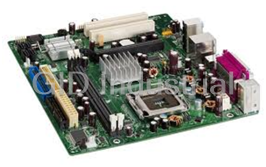
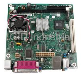
Intel D39287-002 CPU Cooler-Intel CPU Socket 604 Copper Cooler
Request a Quote

The quote request has been received
Close

Facing challenges or have inquiries? Feel free to contact us!
Call Us +1-469-283-2440
What they say about us
FANTASTIC RESOURCE
One of our top priorities is maintaining our business with precision, and we are constantly looking for affiliates that can help us achieve our goal. With the aid of GID Industrial, our obsolete product management has never been more efficient. They have been a great resource to our company, and have quickly become a go-to supplier on our list!
Bucher Emhart Glass
EXCELLENT SERVICE
With our strict fundamentals and high expectations, we were surprised when we came across GID Industrial and their competitive pricing. When we approached them with our issue, they were incredibly confident in being able to provide us with a seamless solution at the best price for us. GID Industrial quickly understood our needs and provided us with excellent service, as well as fully tested product to ensure what we received would be the right fit for our company.
Fuji
HARD TO FIND A BETTER PROVIDER
Our company provides services to aid in the manufacture of technological products, such as semiconductors and flat panel displays, and often searching for distributors of obsolete product we require can waste time and money. Finding GID Industrial proved to be a great asset to our company, with cost effective solutions and superior knowledge on all of their materials, it’d be hard to find a better provider of obsolete or hard to find products.
Applied Materials
CONSISTENTLY DELIVERS QUALITY SOLUTIONS
Over the years, the equipment used in our company becomes discontinued, but they’re still of great use to us and our customers. Once these products are no longer available through the manufacturer, finding a reliable, quick supplier is a necessity, and luckily for us, GID Industrial has provided the most trustworthy, quality solutions to our obsolete component needs.
Nidec Vamco
TERRIFIC RESOURCE
This company has been a terrific help to us (I work for Trican Well Service) in sourcing the Micron Ram Memory we needed for our Siemens computers. Great service! And great pricing! I know when the product is shipping and when it will arrive, all the way through the ordering process.
Trican Well Service
GO TO SOURCE
When I can't find an obsolete part, I first call GID and they'll come up with my parts every time. Great customer service and follow up as well. Scott emails me from time to time to touch base and see if we're having trouble finding something.....which is often with our 25 yr old equipment.
ConAgra Foods