

 Manufacturers
INTEL CA810
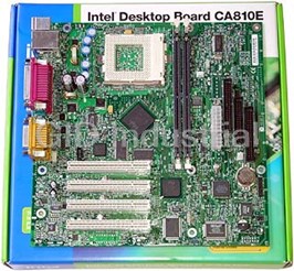
Description
Intel CA810 CPU Board - 810 Chipset Based Motherboard
Part Number
CA810
Price
Request Quote
Manufacturer
INTEL
Lead Time
Request Quote
Category
PRODUCTS - C
Specifications
Audio Subsystem
Creative Sound Blaster
Chipset
Intel810
Expansion Capabilities
our PCI Slots
Form Factor
microATX
Graphics
Intel82810 Graphics/Memory Controller Hub
I/O Control
SMSC LPC47B272
LAN
Intel82559
Memory
Two 168-pin dual inline memory module
Processor
Intel Celeron
Features
- Maximum Memory 512 MB
- Memory Comments PC66/PC100 SDRAM DIMMs
- Memory Expansion 2 sockets
- tandard Memory 0 MB (removable)
Datasheet

Extracted Text
®
Intel CA810 Motherboard
Technical Product Specification
May 1999
Order Number 733082-001
The Intel CA810 motherboard may contain design defects or errors known as errata that may cause the product to deviate from published specifications. Current characterized
errata are documented in the CA810 Motherboard Specification Update.
Revision History
Revision Revision History Date
001 Final release of the CA810 Motherboard Technical Product Specification. May 1999
This product specification applies only to standard CA810 motherboards with BIOS identifier
8C1A100A.86A. For BIOS Setup screen information for motherboards with BIOS identifier
8C1A100A.86R, refer to Section 4.1 on page 79. Other information in this specification applies to
motherboards with either BIOS identifier 8C1A100A.86A or 8C1A100A.86R.
Changes to this specification will be published in the CA810 Motherboard Specification Update
before being incorporated into a revision of this document.
Information in this document is provided in connection with Intel products. No license, express or implied, by estoppel or
otherwise, to any intellectual property rights is granted by this document. Except as provided in Intel’s Terms and
Conditions of Sale for such products, Intel assumes no liability whatsoever, and Intel disclaims any express or implied
warranty, relating to sale and/or use of Intel products including liability or warranties relating to fitness for a particular
purpose, merchantability, or infringement of any patent, copyright or other intellectual property right. Intel products are not
intended for use in medical, life saving, or life sustaining applications.
Intel may make changes to specifications and product descriptions at any time, without notice.
The CA810 motherboard may contain design defects or errors known as errata that may cause the product to deviate from
published specifications. Current characterized errata are available on request.
Contact your local Intel sales office or your distributor to obtain the latest specifications before placing your product order.
Copies of documents which have an ordering number and are referenced in this document, or other Intel literature, may be
obtained from:
Intel Corporation
P.O. Box 5937
Denver, CO 80217-9808
or call in North America 1-800-548-4725, Europe 44-0-1793-431-155, France 44-0-1793-421-777,
Germany 44-0-1793-421-333, other Countries 708-296-9333.
†
Third party brands and names are the property of their respective owners.
Copyright Intel Corporation, 1999.
Preface
This Technical Product Specification (TPS) specifies the board layout, components, connectors,
®
power and environmental requirements, and BIOS for the Intel CA810 motherboard. It describes
the standard motherboard product and available manufacturing options.
Intended Audience
The TPS is intended to provide detailed, technical information about the motherboard and its
components to the vendors, system integrators, and other engineers and technicians who need this
level of information. It is specifically not intended for general audiences.
What This Document Contains
Chapter Description
1 A description of the hardware used on this board
2 A map of the resources of the board
3 The features supported by the BIOS Setup program
4 The contents of the BIOS Setup program’s menus and submenus
5 A description of the BIOS error messages, beep codes, and Power On Self Tests
(POST) codes
6 A list of where to find information about specifications supported by the
motherboard
Typographical Conventions
This section contains information about the conventions used in this specification. Not all of these
symbols and abbreviations appear in all specifications of this type.
Notes, Cautions, and Warnings
NOTE
�
Notes call attention to important information.
CAUTION
Cautions are included to help you avoid damaging hardware or losing data.
WARNING
Warnings indicate conditions that, if not observed, can cause personal injury.
iii
CA810 Motherboard Technical Product Specification
Other Common Notation
Indicates a feature that is implemented—at least in part—on a riser card.
‡
# Used after a signal name to identify an active-low signal (such as USBP0#).
(NxnX) When used in the description of a component, N indicates component type, xn are the relative
coordinates of its location on the motherboard, and X is the instance of the particular part at that
general location. For example, J5J1 is a connector, located at 5J. It is the first connector in the
5J area.
KB Kilobyte (1024 bytes).
Kbit Kilobit (1024 bits).
MB Megabyte (1,048,576 bytes).
Mbit Megabit (1,048,576 bits).
GB Gigabyte (1,073,741,824 bytes).
xxh An address or data value ending with a lowercase h indicates a hexadecimal value.
x.x V Volts. Voltages are DC unless otherwise specified.
†
This symbol is used to indicate third-party brands and names that are the property of their
respective owners.
iv
Contents
1 Motherboard Description
1.1 Overview ................................................................................................................... 12
1.2 Motherboard Layout .................................................................................................. 14
1.3 Processor .................................................................................................................. 16
1.4 System Memory......................................................................................................... 16
1.5 Chipset ......................................................................................................................17
1.6 USB........................................................................................................................... 18
1.7 IDE Support............................................................................................................... 18
1.8 Real-Time Clock, CMOS SRAM, and Battery ............................................................ 19
1.9 I/O Controller ............................................................................................................. 19
1.9.1 Serial Port ................................................................................................... 20
1.9.2 Infrared Support .......................................................................................... 20
1.9.3 Parallel Port................................................................................................. 20
1.9.4 Diskette Drive Controller.............................................................................. 20
1.9.5 Keyboard and Mouse Interface ................................................................... 21
1.10 Graphics Subsystem ................................................................................................. 21
®
1.10.1 Intel 82810 GMCH..................................................................................... 21
1.10.2 Intel 82810 GMCH DC-100 (Optional)......................................................... 22
1.11 Audio Subsystem....................................................................................................... 23
1.11.1 Creative Sound Blaster AudioPCI 64V Audio Controller .............................. 23
1.11.2 Crystal Semiconductor CS4297 Stereo Audio Codec.................................. 23
1.11.3 Audio Connectors........................................................................................ 23
1.12 Hardware Management Features (Optional).............................................................. 24
1.12.1 Hardware Monitor Component .................................................................... 25
1.12.2 Alert on LAN Component............................................................................. 25
1.12.3 Chassis Intrusion Detect Connector ............................................................ 25
1.13 SCSI Hard Drive Activity LED Connector (Optional) .................................................. 25
1.14 LAN Subsystem (Optional) ........................................................................................ 26
1.14.1 Intel 82559 LAN Controller ........................................................................ 26
1.14.2 LAN Subsystem Software............................................................................ 26
1.14.3 RJ-45 LAN Connector LEDs........................................................................ 27
1.15 Power Management Features.................................................................................... 27
1.15.1 Software Support ........................................................................................ 27
1.15.2 Hardware Support ....................................................................................... 30
1.16 Fan Connectors......................................................................................................... 33
1.17 Motherboard Connectors........................................................................................... 34
1.17.1 Back Panel Connectors............................................................................... 35
1.17.2 Midboard Connectors.................................................................................. 39
1.17.3 Front Panel Connectors .............................................................................. 50
1.18 Jumper Blocks........................................................................................................... 53
1.18.1 BIOS Setup Configuration Jumper Block..................................................... 54
1.18.2 USB Port 0 Configuration Jumper Block (Optional) ..................................... 54
v
CA810 Motherboard Technical Product Specification
1.19 Mechanical Considerations........................................................................................ 55
1.19.1 Form Factor................................................................................................. 55
1.19.2 I/O Shield .................................................................................................... 56
1.20 Electrical Considerations ........................................................................................... 57
1.20.1 Power Consumption.................................................................................... 57
1.20.2 Add-in Board Considerations....................................................................... 58
1.20.3 Fan Power Requirements............................................................................ 58
1.20.4 Power Supply Considerations...................................................................... 58
1.21 Thermal Considerations............................................................................................. 59
1.22 Reliability ................................................................................................................... 60
1.23 Environmental Specifications..................................................................................... 61
1.24 Regulatory Compliance ............................................................................................. 62
1.24.1 Safety Regulations ...................................................................................... 62
1.24.2 Safety Regulations ...................................................................................... 62
1.24.3 Certification Markings.................................................................................. 63
2 Motherboard Resources
2.1 Memory Map ............................................................................................................. 65
2.2 DMA Channels .......................................................................................................... 65
2.3 I/O Map ..................................................................................................................... 66
2.4 PCI Configuration Space Map ................................................................................... 68
2.5 Interrupts ...................................................................................................................68
2.6 PCI Interrupt Routing Map......................................................................................... 69
3 Overview of BIOS Features
3.1 Introduction................................................................................................................ 71
3.2 BIOS Flash Memory Organization ............................................................................. 72
3.3 Resource Configuration............................................................................................. 72
3.3.1 PCI Autoconfiguration ................................................................................. 72
3.3.2 PCI IDE Support.......................................................................................... 73
3.4 System Management BIOS (SMBIOS) ...................................................................... 73
3.5 BIOS Upgrades ......................................................................................................... 74
3.5.1 Language Support....................................................................................... 74
3.5.2 Custom Splash Screen................................................................................ 74
3.6 Recovering BIOS Data .............................................................................................. 74
3.7 Boot Options.............................................................................................................. 75
3.7.1 CD-ROM and Network Boot ........................................................................ 75
3.7.2 Booting Without Attached Devices .............................................................. 75
3.7.3 Default Settings After Battery and Power Failure ........................................ 75
3.8 USB Legacy Support ................................................................................................. 76
3.9 BIOS Security Features............................................................................................. 77
vi
Contents
4 BIOS Setup Program
4.1 Introduction................................................................................................................ 79
4.2 Maintenance Menu .................................................................................................... 80
4.3 Main Menu................................................................................................................. 80
4.4 Advanced Menu......................................................................................................... 81
4.4.1 Boot Setting Configuration Submenu .......................................................... 81
4.4.2 Peripheral Configuration Submenu.............................................................. 82
4.4.3 IDE Configuration........................................................................................ 83
4.4.4 IDE Configuration Submenus ...................................................................... 84
4.4.5 Diskette Configuration Submenu................................................................. 85
4.4.6 Event Log Configuration.............................................................................. 85
4.5 Security Menu............................................................................................................ 86
4.6 Power Menu .............................................................................................................. 86
4.7 Boot Menu................................................................................................................. 87
4.8 Exit Menu .................................................................................................................. 88
5 Error Messages and Beep Codes
5.1 BIOS Error Messages................................................................................................ 89
5.2 Port 80h POST Codes............................................................................................... 91
5.3 Bus Initialization Checkpoints .................................................................................... 95
5.4 Speaker..................................................................................................................... 96
5.5 BIOS Beep Codes ..................................................................................................... 96
5.6 Enhanced Diagnostics (Optional) .............................................................................. 97
6 Specifications and Customer Support
6.1 Online Support........................................................................................................... 99
6.2 Specifications ............................................................................................................ 99
Figures
1. microATX Motherboard Components......................................................................... 14
2. Motherboard Block Diagram ...................................................................................... 15
3. Intel 810 Chipset Block Diagram................................................................................ 17
4. Using the Wake on LAN Technology Connector........................................................ 31
5. Location of Standby Power Indicator LED ................................................................. 32
6. Connector Groups ..................................................................................................... 34
7. Back Panel Connectors and Indicators...................................................................... 35
8. Midboard Audio Connectors ...................................................................................... 40
9. Peripheral Interface Connectors ................................................................................ 42
10. Hardware Management and Power Connectors ........................................................ 45
11. PCI Bus Add-In Board Connectors ............................................................................ 48
12. Front Panel Connectors............................................................................................. 50
13. Location of the Jumper Blocks................................................................................... 53
14. Motherboard Dimensions........................................................................................... 55
15. Back Panel I/O Shield Dimensions (microATX Chassis - Independent) ..................... 56
16. Thermally-sensitive Components............................................................................... 59
17. Memory Map of the Flash Memory Device ................................................................ 72
18. Enhanced Diagnostics LEDs ..................................................................................... 97
vii
CA810 Motherboard Technical Product Specification
Tables
1. Processors Supported by the Motherboard ............................................................... 16
2. Intel 82810 GMCH Refresh Rates ............................................................................. 22
3. RJ-45 LAN Connector LEDs...................................................................................... 27
4. Effects of Pressing the Power Switch ........................................................................ 28
5. Power States and Targeted System Power ............................................................... 29
6. Wake Up Devices and Events ................................................................................... 30
7. PS/2 Keyboard/Mouse Connectors............................................................................ 36
8. RJ-45 LAN Connector (optional)................................................................................ 36
9. USB Connectors........................................................................................................ 36
10. Serial Port Connector ................................................................................................ 36
11. Parallel Port Connector.............................................................................................. 37
12. VGA Connector ......................................................................................................... 37
13. MIDI/Game Port Connector ....................................................................................... 38
14. Audio Line-In Connector ............................................................................................ 38
15. Audio Line-Out Connector ......................................................................................... 38
16. Audio Mic-In Connector ............................................................................................. 38
17. ATAPI CD-ROM Connector (J2C2) ........................................................................... 41
18. Optional Video Source Line In Connector (J2C1) ...................................................... 41
19. Optional Legacy CD-ROM Connector (J1C1) ............................................................ 41
20. Optional Auxiliary Line In Connector (J2D2) .............................................................. 41
21. Optional Telephony Connector (J2D3)....................................................................... 41
22. Serial Port B Connector (J2D1) ................................................................................. 43
23. Optional USB Front Panel Connector (J8C1)............................................................. 43
24. Optional SCSI Hard Drive Activity LED Connector (J8A2) (optional) ......................... 43
25. Diskette Drive Connector (J9E1) ............................................................................... 43
26. PCI IDE Connectors (J9D1, J9F1)............................................................................. 44
27. Fan 3 (Processor) Connector (J3J1).......................................................................... 46
28. Optional Fan 2 Connector (J7G1).............................................................................. 46
29. Power Connector (J8D1) ........................................................................................... 46
30. Fan 1 (Chassis Fan) Connector (J9C1) ..................................................................... 46
31. Optional Wake on LAN Technology Connector (J8A3) .............................................. 47
32. Optional Chassis Intrusion Connector (J7B1) ............................................................ 47
33. PCI Bus Connectors .................................................................................................. 49
34. Front Panel Connector (J10B1) ................................................................................. 51
35. Power LED (Single-colored) ...................................................................................... 51
36. Power LED (Dual-colored)......................................................................................... 51
37. Power LED Front Panel Connector (J9A2) ................................................................ 52
38. BIOS Setup Configuration Jumper Settings............................................................... 54
39. USB Port 0 Configuration Jumper Settings................................................................ 54
40. Power Usage............................................................................................................. 57
41. Standby Current Usage ............................................................................................. 58
42. Fan 3 (Processor Fan) DC Power Requirements....................................................... 58
43. Thermal Considerations for Components .................................................................. 60
44. Environmental Specifications..................................................................................... 61
45. Safety Regulations .................................................................................................... 62
46. EMC Regulations....................................................................................................... 62
viii
Contents
47. System Memory Map................................................................................................. 65
48. DMA Channels .......................................................................................................... 65
49. I/O Map ..................................................................................................................... 66
50. PCI Configuration Space Map ................................................................................... 68
51. Interrupts ...................................................................................................................68
52. PCI Interrupt Routing Map......................................................................................... 69
53. Supervisor and User Password Functions ................................................................. 77
54. Setup Menu Bar......................................................................................................... 79
55. Setup Function Keys.................................................................................................. 80
56. Maintenance Menu .................................................................................................... 80
57. Main Menu................................................................................................................. 80
58. Advanced Menu......................................................................................................... 81
60. Peripheral Configuration Submenu............................................................................ 82
61. IDE Device Configuration .......................................................................................... 83
62. IDE Configuration Submenus .................................................................................... 84
63. Diskette Configuration Submenu ............................................................................... 85
64. Event Log Configuration Submenu ............................................................................ 85
65. Security Menu............................................................................................................ 86
66. Power Menu .............................................................................................................. 86
67. Boot Menu................................................................................................................. 87
68. Exit Menu .................................................................................................................. 88
69. BIOS Error Messages................................................................................................ 89
70. Uncompressed INIT Code Checkpoints..................................................................... 91
71. Boot Block Recovery Code Checkpoints ................................................................... 91
72. Runtime Code Uncompressed in F000 Shadow RAM ............................................... 92
73. Beep Codes............................................................................................................... 96
74. Diagnostic LED Codes............................................................................................... 98
75. Compliance with Specifications ................................................................................. 99
ix
CA810 Motherboard Technical Product Specification
x
1 Motherboard Description
What This Chapter Contains
1.1 Overview ................................................................................................................... 12
1.2 Motherboard Layout .................................................................................................. 14
1.3 Processor .................................................................................................................. 16
1.4 System Memory......................................................................................................... 16
1.5 Chipset ......................................................................................................................17
1.6 USB........................................................................................................................... 18
1.7 IDE Support............................................................................................................... 18
1.8 Real-Time Clock, CMOS SRAM, and Battery ............................................................ 19
1.9 I/O Controller ............................................................................................................. 19
1.10 Graphics Subsystem ................................................................................................. 21
1.11 Audio Subsystem....................................................................................................... 23
1.12 Hardware Management Features (Optional).............................................................. 24
1.13 SCSI Hard Drive Activity LED Connector (Optional) .................................................. 25
1.14 LAN Subsystem (Optional) ........................................................................................ 26
1.15 Power Management Features.................................................................................... 27
1.16 Fan Connectors......................................................................................................... 33
1.17 Motherboard Connectors........................................................................................... 34
1.18 Jumper Blocks........................................................................................................... 53
1.19 Mechanical Considerations........................................................................................ 55
1.20 Electrical Considerations ........................................................................................... 57
1.21 Thermal Considerations............................................................................................. 59
1.22 Reliability ................................................................................................................... 60
1.23 Environmental Specifications..................................................................................... 61
1.24 Regulatory Compliance ............................................................................................. 62
11
CA810 Motherboard Technical Product Specification
1.1 Overview
The CA810 motherboard’s features are summarized below.
Form Factor microATX (9.6 inches by 9.6 inches)
® ™
Processor Support for Intel Celeron processor, in a 370-pin PPGA socket, with
66 MHz host bus speed
®
Chipset The Intel 810 chipset consisting of:
®
• Intel 82810 Graphics/Memory Controller Hub (GMCH)
®
• Intel 82801AA I/O Controller Hub (ICH)
®
• Intel 82802AB Firmware Hub (FWH)
Memory • Two 168-pin dual inline memory module (DIMM) sockets
• Support for up to 512 MB of 100-MHz, non-ECC, unbuffered synchronous
DRAM (SDRAM)
32 MB to 256 MB using 16 MB/64 Mbit technology
512 MB maximum using 128 Mbit technology
• Support for serial presence detect (SPD) and non-SPD DIMMs
I/O Control SMSC LPC47B272 low pin count (LPC) interface super I/O controller
Peripheral Interfaces • Two serial ports
• Two USB ports
• One parallel port
• PS/2 keyboard
• PS/2 mouse
†
Audio Subsystem • Creative Sound Blaster AudioPCI 64V audio controller
• AC ‘97 Crystal Semiconductor CS4297 stereo audio codec
Graphics Subsystem • Intel 82810 Graphics/Memory Controller Hub (integrated in the chipset)
Expansion Capabilities • Four PCI slots
BIOS • Intel/AMI BIOS
• Intel 82802AB Firmware Hub (FWH) 4 Mbit flash memory
• Support for SMBIOS, Advanced Configuration and Power Management
Interface (ACPI), Advanced Power Management (APM), and Plug and Play
(see Section 6.2 for specification compliance levels)
Other Features • Speaker
12
Motherboard Description
Not all of the following manufacturing options are available in all marketing channels. Please
contact your Intel representative to determine what manufacturing options are available to you.
Manufacturing Options
Audio
Sony/Phillips digital interface format (S/P-DIF) connector
Chassis Intrusion
Support for chassis intrusion detection
Fan Connector
The fan 2 connector is optional
Hardware Monitor • Wired for Management (WfM) compliant
Subsystem
(see section 6.2 for compliance level)
• Voltage sensor to detect out of range values
Graphics Subsystem Intel 82810 DC-100 Graphics/Memory Controller Hub with support for 1 M x 16
(4 MB) display cache
Enhanced Diagnostics Embedded diagnostics and LEDs that supplement beep codes during POST
®
LAN Controller • Intel 82559 PCI LAN controller with RJ-45 LAN connector
†
• Wake on LAN technology
13
CA810 Motherboard Technical Product Specification
1.2 Motherboard Layout
Figure 1 shows the major components of the CA810 motherboard.
B C E G
A D F H I
J
K
LL
KK
L
JJ
II M
HH
N
GG
FF
EE
O
DD
P
CC
BB
AA Y W V T R
Z X U S Q
OM07766
A Crystal Semiconductor CS4297 audio codec T Power supply connector
B ATAPI-style CD-ROM connector U Fan 1 (chassis) connector
C Video source line in connector (optional) V USB Port 0 front panel connector (optional)
D Legacy CD-ROM connector (optional) W Battery
E Serial port B header X Front panel connector
F Auxiliary line in connector (optional) Y SCSI HD activity LED connector (optional)
G Telephony connector (optional) Z Intel 82802AB Firmware Hub (FWH)
H Enhanced diagnostics LEDs (optional) AA Speaker
I Back panel connectors BB Power LED
J Intel 82559 LAN controller (optional) CC Wake on LAN technology connector (optional)
K Fan 3 (processor) connector DD SMSC LPC47B272 super I/O controller
L 370-pin PPGA processor socket EE Chassis intrusion connector (optional)
M Intel 82810 Graphics/Memory Controller Hub FF Configuration jumper block
(GMCH)
N DIMM sockets GG USB Port 1 front panel configuration jumper
(optional)
O Hardware monitor (optional) HH Creative Sound Blaster AudioPCI 64V audio
controller
P Fan 2 connector (optional) II Intel 82801AA I/O Controller Hub (ICH)
Q Secondary IDE connector JJ S/P-DIF connector (optional)
R Primary IDE connector KK Video memory (optional)
S Diskette drive connector LL PCI slots
Figure 1. microATX Motherboard Components
14
Motherboard Description
Figure 2 is a block diagram showing the relationship among the major components.
Power
Intel
Supply
VREG Celeron Clock
Connector
Processor
100 MHz
FSB (66 MHz)
Clock
1M x 16 SDRAM
4 MB
DIMM 2
Display
SDRAM
1M x 16 SDRAM
Graphics Memory
Cache
100 MHz
Controller Hub DIMM 1
(GMCH)
Hardware SMBus
Hub Link
Monitor (66 MHz)
Wake on LAN
Technology
Connector SMBus
Intel
Primary IDE
82559
I/O
Connector
Controller Hub
PCI Bus
Secondary IDE
(ICH) (33 MHz)
Connector
PCI Slot 1
Diskette Drive
Audio Digital
Firmware Hub
PCI Slot 2
Connector
Controller
(FWH)
PCI Slot 3
Intel 82810 Chipset
PCI Slot 4
Low Pin Count
Super I/O
AC ’97
Controller
MIDI/Game Port
Audio Codec
RJ-45
Amp
PS/2 Mouse/ Parallel (1)
USB Port 0
Diagnostic
Keyboard Serial (2)
LEDs
USB Port 1
Connectors Connectors
OM07757
Figure 2. Motherboard Block Diagram
15
Low Pin Count Bus
CD-ROM
Line In
Audio In
Mic In
Telephone In
Line Out
10/100 Mbps
Ethernet
CA810 Motherboard Technical Product Specification
1.3 Processor
The motherboard supports a single Celeron processor. The processor’s VID pins automatically
program the voltage regulator on the motherboard to the required processor voltage. The host bus
speed of 66 MHz is automatically selected. The processor connects to the motherboard through
the 370-pin PPGA socket.
The motherboard supports the processors listed in Table 1.
Table 1. Processors Supported by the Motherboard
Processor Speed Host Bus Frequency Cache Size
333 MHz 66 MHz 128 KB
366 MHz 66 MHz 128 KB
400 MHz 66 MHz 128 KB
433 MHz 66 MHz 128 KB
466 MHz 66 MHz 128 KB
All supported onboard memory can be cached.
For the latest information on processor support for the CA810 motherboard, refer to the Intel
boxed motherboard web site at:
http://support.intel.com/support/motherboards/desktop/
1.4 System Memory
The motherboard has two DIMM sockets. SDRAM can be installed in one or both sockets.
Minimum memory size is 32 MB; maximum memory size is 512 MB. The BIOS automatically
detects memory type, size, and speed. Due to the video requirements of the CA810 motherboard,
†
minimum memory for the Windows NT 4.0 operating system is 64 MB.
NOTE
�
Processors with 66 MHz host bus can be paired with either 66 MHz or 100 MHz SDRAM.
The motherboard supports memory with the following features:
• 168-pin DIMMs with gold-plated contacts
• 100 MHz unbuffered SDRAM
• Non-ECC (64-bit) memory
• 100 MHz memory may be either Serial Presence Detect (SPD) or non-SPD memory
• 3.3 V memory only
CAUTION
Because the main system memory is also used as video memory, the CA810 motherboards require
100 MHz SDRAM DIMMs even though the processor front side bus is 66 MHz. It is highly
recommended that SPD DIMMs be used, since this allows the chipset to accurately configure
memory settings for optimum performance. If non-SPD memory is installed, the BIOS will attempt
to correctly configure the memory settings, but performance and reliability may be impacted.
16
Motherboard Description
The motherboard supports single- or double-sided DIMMs in the following sizes:
DIMM Size Non-ECC Configuration
16 MB 2 Mbit x 64
32 MB 4 Mbit x 64
64 MB 8 Mbit x 64
128 MB 16 Mbit x 64
256 MB 32 Mbit x 64
NOTE
�
All memory components and DIMMs used with the CA810 motherboard must comply with
the PC SDRAM Unbuffered DIMM Specification. You can access this document through the
Internet at:
http://www.intel.com/design/chipsets/memory/index.htm
See Section 6.2 for information about this SDRAM DIMM specification.
1.5 Chipset
The Intel 810 chipset consists of the following devices:
• Graphics Memory Controller Hub (GMCH)
• I/O Controller Hub (ICH)
• Firmware Hub (FWH)
The chipset provides the host, memory, graphics, and I/O interfaces shown in Figure 3.
For information about the Intel 810 chipset, refer to the Intel web site at:
http://developer.intel.com
Host Bus ATA33/66 USB
810 Chipset
82810
100 MHz 82802AB
Graphics Memory Hub 82801AA I/O Controller Hub
SDRAM Firmware Hub
Controller Hub Link (ICH)
Bus (FWH)
(GMCH)
SM Bus
PCI Bus
LPC Bus
Display
AC Link
Interface
OM08814
Figure 3. Intel 810 Chipset Block Diagram
17
CA810 Motherboard Technical Product Specification
1.6 USB
The motherboard has two USB ports; one USB peripheral can be connected to each port. For more
than two USB devices, an external hub can be connected to either port. The two USB ports are
implemented with stacked back panel connectors. The motherboard fully supports UHCI and uses
UHCI-compatible software drivers. See Section 6.2 for information about the USB and UHCI
specifications.
USB features include:
• Self-identifying peripherals that can be plugged in while the computer is running
• Automatic mapping of function to driver and configuration
• Support for isochronous and asynchronous transfer types over the same set of wires
• Support for up to 127 physical devices
• Guaranteed bandwidth and low latencies appropriate for telephony, audio, and other
applications
• Error-handling and fault-recovery mechanisms built into the protocol
NOTE
�
Computer systems that have an unshielded cable attached to a USB port may not meet FCC
Class B requirements, even if no device or a low-speed USB device is attached to the cable. Use
shielded cable that meets the requirements for full-speed devices.
1.7 IDE Support
The motherboard has two independent bus-mastering IDE interfaces. These interfaces support:
• ATAPI devices (such as CD-ROM drives)
• Ultra ATA/33 and Ultra ATA/66 devices
The BIOS supports logical block addressing (LBA) and extended cylinder head sector (ECHS)
translation modes. The drive reports the transfer rate and translation mode to the BIOS.
The motherboard supports laser servo (LS-120) diskette technology through its IDE interfaces.
The LS-120 drive can be configured as a boot device by setting the BIOS Setup program’s Boot
Device Menu (see Section 4.7) to one of the following:
• ARMD-FDD (ATAPI Removable Media Device - Floppy Disk Drive)
• ARMD-HDD (ATAPI Removable Media Device - Hard Disk Drive)
18
Motherboard Description
1.8 Real-Time Clock, CMOS SRAM, and Battery
The real-time clock is compatible with DS1287 and MC146818 components. The clock provides a
time-of-day clock and a multicentury calendar with alarm features and century rollover. The real-
time clock supports 256 bytes of battery-backed CMOS SRAM in two banks that are reserved for
BIOS use.
The time, date, and CMOS values can be specified in the Setup program. The CMOS values can
be returned to their defaults by using the Setup program.
NOTE
�
The recommended method of accessing the date in systems with Intel motherboards is from the
Real-Time Clock (RTC) via the BIOS. The BIOS on Intel motherboards contains a century
checking and maintenance feature that checks the least two significant digits of the year stored in
the RTC during each BIOS request (INT 1Ah). During this check, the BIOS reads the date and, if
less than 80 (i.e., 1980 is the first year supported by the PC), updates the century byte to 20. This
feature enables operating systems and applications using the BIOS date/time services to reliably
manipulate the year as a four-digit value.
For more information on proper date access in systems with Intel motherboards, please see
http://support.intel.com/support/year2000/motherboard.htm
A coin-cell battery powers the real-time clock and CMOS memory. When the computer is not
plugged into a wall socket, the battery has an estimated life of three years. When the computer is
plugged in, the 3.3 V standby current extends the life of the battery. The clock is accurate to
± 13 minutes/year at 25 ºC with 3.3 V applied.
1.9 I/O Controller
The SMSC LPC47B272 super I/O controller provides the following features:
• Low pin count (LPC) interface
• Two serial ports
†
• Infrared port (IrDA 1.1 compliant)
• One parallel port with Extended Capabilities Port (ECP) and Enhanced Parallel Port (EPP)
support
• PS/2–style mouse and keyboard interfaces
• Interface for one 1.2 MB, 1.44 MB, or 2.88 MB diskette drive
• Intelligent power management, including a programmable wake up event interface
• Fan control:
Two pulse width modulation (PWM) fan speed control outputs
Two fan tachometer inputs
The BIOS Setup program provides configuration options for the I/O controller.
19
CA810 Motherboard Technical Product Specification
1.9.1 Serial Port
The motherboard has one 9-pin D-Sub serial port connector located on the back panel and an
optional connector on the board for a second serial port. The serial ports’ NS16C550-compatible
UARTs support data transfers at speeds up to 115.2 Kbits/sec with BIOS support. The serial ports
can be assigned as COM1 (3F8h), COM2 (2F8h), COM3 (3E8h), or COM4 (2E8h).
1.9.2 Infrared Support
On the front panel connector, there are four pins that support Hewlett Packard HSDL-1000
compatible infrared (IR) transmitters and receivers. In the BIOS Setup program, Serial Port B can
be directed to a connected IR device. (In this case, the Serial Port B connector on the back panel
cannot be used.) The IR connection can be used to transfer files to or from portable devices like
laptops, PDAs, and printers. The Infrared Data Association (IrDA) specification supports data
transfers of 115 Kbits/sec at a distance of 1 meter. For information about the IrDA specification,
see Section 6.2.
1.9.3 Parallel Port
The connector for the multimode bidirectional parallel port is a 25-pin D-Sub connector located on
the back panel of the motherboard. In the Setup program, there are four options for parallel port
operation:
• Output Only
• Bidirectional (PS/2 compatible)
• EPP
• ECP
1.9.4 Diskette Drive Controller
The I/O controller supports a single diskette drive that is compatible with the 82077 diskette drive
†
controller and supports both PC-AT or PS/2 modes. For information about the diskette drive
capacities and sizes, see Table 63 on page 85.
NOTE
�
The I/O controller supports 1.2 MB, 3.5-inch diskette drives, but a special driver is required for
this type of drive.
20
Motherboard Description
1.9.5 Keyboard and Mouse Interface
PS/2 keyboard and mouse connectors are located on the back panel of the motherboard. The
†
+5 V lines to these connectors are protected with a PolySwitch circuit that, like a self-healing
fuse, reestablishes the connection after an overcurrent condition is removed.
NOTE
�
The mouse and keyboard can be plugged into either PS/2 connector. Power to the computer
should be turned off before a keyboard or mouse is connected or disconnected.
The keyboard controller contains code that provides the traditional keyboard and mouse control
functions and also supports Power On/Reset password protection. A Power On/Reset password
can be specified in the BIOS Setup program.
1.10 Graphics Subsystem
The graphics subsystem features the Intel 82810 Graphics/Memory Controller Hub (GMCH).
Visit Intel’s World Wide Web (see Section 6.2) site for information about graphics drivers.
®
1.10.1 Intel 82810 GMCH
The Intel 82810 GMCH features the following:
• Integrated graphics controller
3-D Hyper Pipelined architecture
Full 2-D hardware acceleration
Motion video acceleration
• 3-D graphics visual and texturing enhancements
• Display
Integrated 24-bit 230 MHz RAMDAC
Display Data Channel Standard, Version 3.0, Level 2B protocols compliant
(see Section 6.2 for specification information)
• Video
Hardware motion compensation for software MPEG2 decode
Software DVD at 30 fps
• Integrated graphics memory controller
21
CA810 Motherboard Technical Product Specification
Table 2 lists the refresh rates supported by the CA810 motherboard.
Table 2. Intel 82810 GMCH Refresh Rates
Resolution Color 60 (Hz) 70 (Hz) 72 (Hz) 75 (Hz) 85 (Hz)
640x200 16 x
640x350 16 x
640x400 256 x x x x
64 K x x x x
16 M x
640x480 16 x x x x
256 x x x x x
32 K x x x
64 K x x x x x
16 M x x x x x
800x600 256 x x x x x
32 K x x x
64 K x x x x x
16 M x x x x x
1024x768 256 x x x x
32 K x x x
64 K x x x x x
16 M x x x x x
1056x800 16 x
1280x1024 256 x x x x x
32 K x x
64 K x x x x x
16 M x x x x x
NOTE
�
Some of the system memory is reserved for video.
1.10.2 Intel 82810 GMCH DC-100 (Optional)
In addition to all the features of the Intel 82810 GMCH, the optional Intel 82810 GMCH DC-100
includes 4 MB of display cache.
See Intel’s World Wide Web site for information about graphics drivers:
http://support.intel.com/support/motherboards/desktop/
22
Motherboard Description
1.11 Audio Subsystem
The Audio Codec ’97 (AC ’97) compatible audio subsystem includes these features:
• Split digital/analog architecture for improved signal-to-noise ratio (≥ 85 dB) measured at line
out, from any analog input, including line in, CD-ROM, and auxiliary line in
• 3-D stereo enhancement
• Power management support for APM 1.2 and ACPI 1.0
The audio subsystem consists of these devices:
• Sound Blaster AudioPCI 64V audio controller
• Crystal Semiconductor CS4297 stereo audio codec
• Audio connectors
1.11.1 Creative Sound Blaster AudioPCI 64V Audio Controller
The Creative Sound Blaster AudioPCI 64V audio controller features:
• Interfaces to PCI bus as a Plug and Play device
• 100% DOS legacy compatible
• Access to main memory (through the PCI bus) for wavetable synthesis support – does not
require a separate wavetable ROM device
• Conforms to the PC 98 and PC 99 design guides
• Optional Sony/Phillips digital interface format (S/P-DIF)
1.11.2 Crystal Semiconductor CS4297 Stereo Audio Codec
The Crystal Semiconductor CS4297 stereo audio codec features:
• High performance 18-bit stereo full-duplex audio codec with up to 48 kHz sampling rate
• Connects to the Sound Blaster AudioPCI 64V using a five-wire digital interface
1.11.3 Audio Connectors
The audio connectors include the following:
• Optional CD-ROM (legacy-style)
• ATAPI-style connectors
CD-ROM
Auxiliary line in (optional)
Telephony (optional)
Video source line in (optional)
• Back panel connectors
Line out
Line in
Mic in
MIDI/Game Port
23
CA810 Motherboard Technical Product Specification
NOTE
�
The line out connector, located on the back panel, is designed to power either headphones or
amplified speakers only. Poor audio quality may occur if passive (non-amplified) speakers are
connected to this output.
1.11.3.1 CD-ROM (Legacy-style 2 mm) Connector (Optional)
A 1 x 4-pin legacy-style 2 mm connector connects an internal CD-ROM drive to the audio mixer.
1.11.3.2 ATAPI CD-ROM Audio Connector
A 1 x 4-pin ATAPI connector connects an internal CD-ROM drive to the audio mixer.
1.11.3.3 Auxiliary Line In Connector (Optional)
A 1 x 4-pin ATAPI-style connector connects the left and right channel signals of an internal audio
device to the audio subsystem.
1.11.3.4 Telephony Connector (Optional)
A 1 x 4-pin ATAPI-style connector connects the monaural audio signals of an internal telephony
device to the audio subsystem. A monaural audio-in and audio-out signal interface is necessary for
telephony applications such as speakerphones, fax/modems, and answering machines.
1.11.3.5 Video Source Line In Connector (Optional)
A 1 x 4 pin ATAPI style connector connects the left and right audio channel signals of an internal
video device to the audio subsystem. An audio-in signal interface of this type is necessary for
applications such as TV tuners.
1.12 Hardware Management Features (Optional)
The optional hardware management features enable the board to be compatible with the Wired for
Management (WfM) specification. The board has several hardware management features,
including the following:
• Hardware monitor component
• Alert on LAN component
• Chassis intrusion detection
• Fan control and monitoring (implemented on the SMSC LPC47B272 I/O controller)
24
Motherboard Description
1.12.1 Hardware Monitor Component
The optional hardware monitor component provides low-cost instrumentation capabilities. The
features of the component include:
• Internal ambient temperature sensing
• Remote thermal diode sensing for direct monitoring of processor temperature
• Power supply monitoring (+12, +5, +3.3, +2.5, VCCP) to detect levels above or below
acceptable values
• SMBus interface
1.12.2 Alert on LAN Component
The optional Alert on LAN component is a companion device to the 82559 LAN controller.
Together, the two devices provide a management interface between a remote console (or
management server) and the client system monitoring instrumentation (the ICH and/or the
hardware monitor component). The functions of the alert on LAN component include:
• Sending alert (SOS), heartbeat, or pong (ping response) packets to the 82559 LAN controller
• Receiving specially filtered packets needed for advanced power management modes such as
reset, power-up, or power-down
1.12.3 Chassis Intrusion Detect Connector
The board supports a chassis security feature that detects if the chassis cover is removed and
sounds an alarm (through the onboard speaker or PC chassis speaker, if either is present). For the
chassis intrusion circuit to function, the chassis’ power supply must be connected to AC power.
The security feature uses a mechanical switch on the chassis that attaches to the chassis intrusion
detect connector. The mechanical switch is closed for normal computer operation.
1.13 SCSI Hard Drive Activity LED Connector (Optional)
The SCSI hard drive activity LED connector is a 1 x 2-pin connector that allows an add-in SCSI
controller to use the same LED as the onboard IDE controller. This connector can be connected to
the LED output of the add-in controller card. The LED will indicate when data is being read or
written using the add-in controller. See Section 1.17.2 for the location and pinouts of the SCSI
hard drive activity LED connector.
25
CA810 Motherboard Technical Product Specification
1.14 LAN Subsystem (Optional)
The Intel 82559 Fast Ethernet Wired for Management (WfM) PCI LAN subsystem provides both
10Base-T and 100Base-TX connectivity. Features include:
• 32-bit, 33 MHz direct bus mastering on the PCI bus
• Shared memory structure in the host memory that copies data directly to/from host memory
• 10Base-T and 100Base-TX capability using a single RJ-45 connector with connection and
activity status LEDs
• IEEE 802.3μ Auto-Negotiation for the fastest available connection
• Jumperless configuration; the LAN subsystem is completely software-configurable
1.14.1 Intel 82559 LAN Controller
The Intel 82559 PCI LAN controller’s features include:
• CSMA/CD Protocol Engine
• PCI bus interface
• DMA engine for movement of commands, status, and network data across the PCI bus
• Integrated physical layer interface, including:
Complete functionality necessary for the 10Base-T and 100Base-TX network interfaces;
when in 10 Mbit/sec mode, the interface drives the cable directly
A complete set of Media Independent Interface (MII) management registers for control
and status reporting
802.3μ Auto-Negotiation for automatically establishing the best operating mode when
connected to other 10Base-T or 100Base-TX devices, whether half- or full-duplex capable
• Integrated power management features, including:
Support for APM
Support for Wake on LAN technology
1.14.2 LAN Subsystem Software
The Intel 82559 Fast Ethernet WfM PCI LAN software and drivers are available from Intel’s
World Wide Web site (see Section 6.1).
26
Motherboard Description
1.14.3 RJ-45 LAN Connector LEDs
Two LEDs are built into the RJ-45 LAN connector. Table 3 describes the LED states when the
board is powered up and the LAN subsystem is operating.
Table 3. RJ-45 LAN Connector LEDs
LED Color LED State Indicates
Green Off 10 Mbit/sec speed is selected.
On 100 Mbit/sec speed is selected.
Yellow Off LAN link is not established.
On (steady state) LAN link is established.
On (brighter and pulsing) The computer is communicating with another computer on
the LAN.
1.15 Power Management Features
Power management is implemented at several levels, including:
• Software support:
Advanced Power Management (APM)
Advanced Configuration and Power Interface (ACPI)
• Hardware support:
Wake on LAN technology (optional)
Instantly Available technology
Resume on Ring
1.15.1 Software Support
The software support for power management includes:
• APM
• ACPI
If the board is used with an ACPI-aware operating system, the BIOS can provide ACPI support.
Otherwise, it defaults to APM support.
27
CA810 Motherboard Technical Product Specification
1.15.1.1 APM
APM makes it possible for the computer to enter an energy saving standby mode. The standby
mode can be initiated in the following ways:
• Time-out period specified in the BIOS Setup program
• Suspend/resume switch connected to the front panel sleep connector
• From the operating system, such as the Suspend menu item in Windows 95
In standby mode, the motherboard can reduce power consumption by spinning down hard drives,
†
and reducing power to or turning off VESA DPMS-compliant monitors. Power-management
mode can be enabled or disabled in the BIOS Setup program.
While in standby mode, the system retains the ability to respond to external interrupts and service
requests, such as incoming faxes or network messages. Any keyboard or mouse activity brings the
system out of standby mode and immediately restores power to the monitor.
The BIOS enables APM by default; but the operating system must support an APM driver for the
power-management features to work. For example, Windows 95 supports the power-management
features upon detecting that APM is enabled in the BIOS.
1.15.1.2 ACPI
ACPI gives the operating system direct control over the power management and Plug and Play
functions of a computer. The use of ACPI with this board requires the support of an operating
system that provides full ACPI functionality. ACPI features include:
• Plug and Play (including bus and device enumeration) and APM functionality normally
contained in the BIOS
• Power management control of individual devices, add-in boards (some add-in boards may
require an ACPI-aware driver), video displays, and hard disk drives
• Methods for achieving less than 30-watt system operation in the Power On Suspend sleeping
state, and less than 5-watt system operation in the Suspend to Disk sleeping state
• A Soft-off feature that enables the operating system to power off the computer
• Support for multiple wake up events (see Table 6 on page 30)
• Support for a front panel power and sleep mode switch. Table 4 lists the system states based
on how long the power switch is pressed, depending on how ACPI is configured with an
ACPI-aware operating system.
Table 4. Effects of Pressing the Power Switch
…and the power switch is
If the system is in this state… pressed for …the system enters this state
Off (ACPI G2/S5 state) Less than four seconds Power on
On (ACPI G0 state) Less than four seconds Soft off/Suspend
On (ACPI G0 state) More than four seconds Fail safe power off
Sleep (ACPI G1 state) Less than four seconds Wake up
Sleep (ACPI G1 state) More than four seconds Power off
28
Motherboard Description
NOTE
�
The Wake on LAN technology connector at location J8A3 is only supported in APM mode. ACPI
mode is not supported.
1.15.1.2.1 System States and Power States
Under ACPI, the operating system directs all system and device power state transitions. The
operating system puts devices in and out of low-power states based on user preferences and
knowledge of how devices are being used by applications. Devices that are not being used can be
turned off. The operating system uses information from applications and user settings to put the
system as a whole into a low-power state.
Table 5 lists the power states supported by the motherboard along with the associated system
power targets. See the ACPI specification for a complete description of the various system and
power states.
Table 5. Power States and Targeted System Power
Global States Sleeping States CPU States Device States Targeted System Power*
G0 - working S0 - working C0 - working D0 - working state Full power > 60 W
state
G1 - sleeping S1 - CPU stopped C1 - stop D1, D2, D3- device 5 W < power < 30 W
state grant specification
specific.
G1 - sleeping S3 - Suspend-to- No power D3 - no power Power < 5W **
state RAM. Context except for wake up
saved to RAM. logic.
G2/S5 S5 - Soft off. No power D3 - no power Power < 5 W **
Context not saved. except for wake up
Cold boot is logic.
required.
G3 - No power to the No power D3 - no power for No power to the system
mechanical off. system. wake up logic, so that service can be
except when performed.
AC power is
provided by battery
disconnected
or external source.
from the
computer.
* Total system power is dependent on the system configuration, including add-in boards and peripherals powered by the
system chassis’ power supply.
** Dependent on the standby power consumption of wake-up devices used in the system.
29
CA810 Motherboard Technical Product Specification
1.15.1.2.2 Wake Up Devices and Events
Table 6 lists the devices or specific events that can wake the computer from specific states.
Sleeping state S5 is the same for the wake up event.
Table 6. Wake Up Devices and Events
These devices/events can wake up the computer… …from this state
Power switch S1, S3, S5
RTC alarm S1, S3, S5
LAN S1, S3, S5
Modem S1, S3, S5
IR command S1
USB S1
PS/2 keyboard S1
PS/2 mouse S1
Sleep button S1
PME S1, S3, S5
1.15.1.2.3 Plug and Play
In addition to power management, ACPI provides controls and information so that the operating
system can facilitate Plug and Play device enumeration and configuration. ACPI is used only to
enumerate and configure motherboard devices that do not have other hardware standards for
enumeration and configuration. PCI devices on the motherboard, for example, are not enumerated
by ACPI.
1.15.2 Hardware Support
The board provides several hardware features that support power management, including:
• Wake on LAN technology (optional)
• Instantly Available technology
• Resume on Ring
Wake on LAN technology and Instantly Available technology require power from the
+5 V standby line. The sections discussing these features describe the incremental standby
power requirements for each.
CAUTION
If Wake on LAN and Instantly Available technology features are used, ensure that the power
supply provides adequate +5 V standby current. Failure to do so can damage the power supply.
The total amount of standby current required depends on the wake devices supported and
manufacturing options.
Resume on Ring enables telephony devices to access the computer when it is in a power-managed
state. The method used depends on the type of telephony device (external or internal) and the
power management mode being used (APM or ACPI).
30
Motherboard Description
NOTE
�
The use of Resume on Ring technology from an ACPI state requires the support of an operating
system that provides full ACPI functionality.
1.15.2.1 Wake on LAN Technology
Wake on LAN technology enables remote wakeup of the computer through a network. The LAN
subsystem, whether onboard or as a PCI bus network adapter, monitors network traffic at the
†
Media Independent Interface. Upon detecting a Magic Packet frame, the LAN subsystem asserts
a wakeup signal that powers up the computer. Depending on the LAN implementation, the
motherboard board supports Wake on LAN technology in one of two ways:
• Through the Wake on LAN technology connector
• Through the PCI bus PME# signal (for PCI 2.2 compliant LAN designs)
The Wake on LAN technology connector can be used with PCI bus network adapters that have a
remote wake up connector, as shown in Figure 4. Network adapters that are PCI 2.2 compliant
assert the wakeup signal through the PCI bus signal PME# (pin A19 on the PCI bus connectors).
The optional onboard LAN subsystem also supports remote wakeup using the PME# signal.
Network
Remote
Interface
Wake up
Wake on
Card
connector
LAN
technology
connector
PCI Slot
Motherboard
OM08815
Figure 4. Using the Wake on LAN Technology Connector
CAUTION
For Wake on LAN technology, the 5-V standby line for the power supply must be capable of
delivering +5 V ± 5% at 720 mA. Failure to provide adequate standby current when implementing
Wake on LAN technology can damage the power supply.
31
CA810 Motherboard Technical Product Specification
1.15.2.2 Instantly Available Technology
Instantly Available technology enables the board to enter the ACPI S3 (Suspend-to-RAM) sleep
state. While in the S3 sleep state, the computer will appear to be off. When signaled by a wake up
device or even, the system quickly returns to its last known wake state. Table 6 on page 30 lists
the devices and events that can wake the computer from the S3 state.
The board supports the PCI Bus Power Management Interface Specification and the 3.3V Aux
ECR. Add-in boards that also support these specifications can participate in power management
and can be used to wake the computer.
The optional standby power indicator (located between the IDE connectors and power connector)
provides an indication that power is still present to the DIMMs and PCI bus connectors, even when
the computer appears to be off. Figure 5 shows the location of the standby power LED.
DS8E1
OM07804
Standby Power Indicator
Figure 5. Location of Standby Power Indicator LED
CAUTION
For Instantly Available technology, the power supply must be capable of providing the
+5 V standby current that those boards require in addition to the standby current required by the
motherboard. Failure to provide adequate standby current when using this feature can damage
the power supply. Refer to Section 1.20.2 for more information.
32
Motherboard Description
1.15.2.3 Resume on Ring
The operation of Resume on Ring can be summarized as follows:
• Resumes operation from either the APM sleep mode or the ACPI S1 state
• Requires only one call to access the computer
• Detects incoming call similarly for external and internal modems; does not use the Wake on
Ring connector
• Requires modem interrupt be unmasked for correct operation
1.16 Fan Connectors
The board has three fan connectors, one being a manufacturing option. The functions of these
connectors are:
• The processor fan (fan 3) connector provides +12 V DC for a processor fan or active fan
heatsink.
• The chassis fan (fan 1) connector provides a high/low control signal for a fan located inside of
and powered by the system power supply.
• The front panel fan (fan 2) connector is optional.
33
CA810 Motherboard Technical Product Specification
1.17 Motherboard Connectors
This section describes the motherboard’s connectors. The connectors can be divided into three
groups, as shown in Figure 6.
Back panel connectors
A
A
(see page 35)
B
Midboard connectors
B
(see page 39)
C
Front panel connectors
(see page 50)
C
OM07764
Figure 6. Connector Groups
CAUTION
Only the back panel connectors of this motherboard have overcurrent protection. The internal
motherboard connectors do not have overcurrent protection; they should connect only to devices
inside the computer chassis, such as fans and internal peripherals. Do not use these connectors
for powering devices external to the computer chassis. A fault in the load presented by the
external devices could cause damage to the computer, the interconnecting cable, and the external
devices themselves.
34
Motherboard Description
1.17.1 Back Panel Connectors
Figure 7 shows the location of the back panel connectors.
C
A
G J
B DE F HIM KL
OM07762
A PS/2 keyboard or mouse H Serial port A
B PS/2 keyboard or mouse I Enhanced diagnostics LEDs (optional)
C RJ-45 LAN (optional) J MIDI/Game port
D USB port 0 (optional) K Audio line-out
E USB port 1 (optional) L Audio line-in
F VGA port M Mic in
G Parallel port
Figure 7. Back Panel Connectors and Indicators
35
CA810 Motherboard Technical Product Specification
Table 7. PS/2 Keyboard/Mouse Connectors
Pin Signal
1Data
2 Not connected
3 Ground
4 Fused +5 V
5Clock
6 Not connected
Table 8. RJ-45 LAN Connector (optional)
Pin Signal Name
1TxD +
2TxD -
3RxD +
4 Ground
5 Ground
6RxD -
7 Ground
8 Ground
Table 9. USB Connectors
Pin Signal
1 Fused +5 V
2 3.3V differential USB signal USB_D–
3 3.3V differential USB signal USB_D+
4 Ground
Table 10. Serial Port Connector
Pin Signal
1 DCD (Data Carrier Detect)
2 SIN# (Serial Data In)
3 SOUT# (Serial Data Out)
4 DTR (Data Terminal Ready)
5 Ground
6 DSR (Data Set Ready)
7 RTS (Request to Send)
8 CTS (Clear to Send)
9 RI (Ring Indicator)
36
Motherboard Description
Table 11. Parallel Port Connector
Pin Std Signal ECP Signal EPP Signal I/O
1 STROBE# STROBE# WRITE# I/O
2 PD0 PD0 PD0 I/O
3 PD1 PD1 PD1 I/O
4 PD2 PD2 PD2 I/O
5 PD3 PD3 PD3 I/O
6 PD4 PD4 PD4 I/O
7 PD5 PD5 PD5 I/O
8 PD6 PD6 PD6 I/O
9 PD7 PD7 PD7 I/O
10 ACK# ACK# INTR I
11 BUSY BUSY#, PERIPHACK WAIT# I
12 PERROR PE, ACKREVERSE# PE I
13 SELECT SELECT SELECT I
14 AUDOFD# AUDOFD#, HOSTACK DATASTB# O
15 FAULT# FAULT#, PERIPHREQST# FAULT# I
16 INIT# INIT#, REVERSERQST# RESET# O
17 SLCTIN# SLCTIN# ADDRSTB# O
18 - 25 GND GND GND -
Table 12. VGA Connector
Pin Signal
1RED
2 GREEN
3BLUE
4 Not connected
5GND
6GND
7GND
8GND
9 FUSED VCC
10 GND
11 Not connected
12 DDC_SDA
13 HSYNC
14 VSYNC
15 DDC_SCL
37
CA810 Motherboard Technical Product Specification
Table 13. MIDI/Game Port Connector
Pin Signal Name Pin Signal Name
1 +5 V (fused) 9 +5 V (fused)
2 GP4 (JSBUT0) 10 GP6 (JSBUT2)
3 GP0 (JSX1) 11 GP2 (JSX2)
4 Ground 12 MIDI-OUT
5 Ground 13 GP3 (JSY2)
6 GP1 (JSY1) 14 GP7 (JSBUT3)
7 GP5 (JSBUT1) 15 MIDI-IN
8 +5 V (fused)
Table 14. Audio Line-In Connector
Pin Signal
Tip Audio left in
Ring Audio right in
Sleeve Ground
Table 15. Audio Line-Out Connector
Pin Signal
Tip Audio left out
Ring Audio right out
Sleeve Ground
Table 16. Audio Mic-In Connector
Pin Signal
Tip Mono in
Ring Mic bias voltage
Sleeve Ground
38
Motherboard Description
1.17.2 Midboard Connectors
The midboard connectors are divided into the following functional groups:
• Audio (see page 40)
Auxiliary line-in (optional)
CD-ROM (ATAPI-style)
CD-ROM (Legacy-style)
Telephony (optional)
Video source line-in (optional)
• Peripheral interfaces (see page 42)
USB front panel (optional)
SCSI HD activity LED (optional)
Diskette drive
IDE (2)
Serial port B
• Hardware Management and Power (see page 45)
Chassis intrusion (optional)
Fans (3)
Power
Wake on LAN technology (optional)
• PCI bus add-in boards (see page 48)
39
CA810 Motherboard Technical Product Specification
1.17.2.1 Audio
Figure 8 shows the location of the audio connectors.
A B C D E
14
1
4 1
1 4
1
OM07771
Reference
Item Description Color Style Designator
A CD-ROM black ATAPI J2C2
B Video source line-in (optional) blue ATAPI J2C1
C CD-ROM (optional) white Legacy, 2 mm J1C1
D Auxiliary line-in (optional) natural ATAPI J2D2
E Telephony (optional) green ATAPI J2D3
Figure 8. Midboard Audio Connectors
40
Motherboard Description
Table 17. ATAPI CD-ROM Connector (J2C2)
Pin Signal
1 Left audio input from CD-ROM
2 CD audio differential ground
3 CD audio differential ground
4 Right audio input from CD-ROM
Table 18. Optional Video Source Line In
Connector (J2C1)
Pin Signal
1 Left auxiliary line in
2 Ground
3 Ground
4 Right auxiliary line in
Table 19. Optional Legacy CD-ROM
Connector (J1C1)
Pin Signal
1 CD audio differential ground
2 Left audio input from CD-ROM
3 CD audio differential ground
4 Right audio input from CD-ROM
Table 20. Optional Auxiliary Line In
Connector (J2D2)
Pin Signal
1 Left auxiliary line in
2 Ground
3 Ground
4 Right auxiliary line in
Table 21. Optional Telephony Connector
(J2D3)
Pin Signal
1 Analog audio mono input
2 Ground
3 Ground
4 Analog audio mono output
41
CA810 Motherboard Technical Product Specification
1.17.2.2 Peripheral Interfaces
Figure 9 shows the location of the peripheral interface connectors.
A
8
2
1 9
12
F
8
1
9
E
240
1 39
2 34
1 33
240
1 39
D C B
OM07770
A Serial port B D Primary IDE
B Secondary IDE E SCSI hard drive activity LED (optional)
C Diskette drive F USB front panel (optional)
Figure 9. Peripheral Interface Connectors
42
Motherboard Description
Table 22. Serial Port B Connector (J2D1)
Pin Signal Pin Signal
1 DCD Data Carrier Detect) 2 DSR (Data Set Ready)
3 SIN# Serial Data In) 4 RTS (Request to Send)
5 SOUT# (Serial Data Out) 6 CTS (Clear to Send)
7 DTR (Data Terminal Ready) 8 RI (Ring Indicator)
9 Ground
Table 23. Optional USB Front Panel Connector (J8C1)
Pin Signal Pin Signal
1 TP_FPUSB_1 2 VCC
3 Ground 4 TP_FUSB_4
5 TP_FPUSB_5 6 FNT_USBP0
7 Ground 8 FNT_USBP0 #
9 Ground
Table 24. Optional SCSI Hard Drive Activity
LED Connector (J8A2) (optional)
Pin Signal
1 SCSI activity
2 Not connected
Table 25. Diskette Drive Connector (J9E1)
Pin Signal Pin Signal
1 Ground 2 DENSEL
3 Ground 4 Reserved
5Key 6FDEDIN
7 Ground 8 FDINDX# (Index)
9 Ground 10 FDM00# (Motor Enable A)
11 Ground 12 No connect
13 Ground 14 FDDS0# (Drive Select A)
15 Ground 16 No connect
17 No connect 18 FDDIR# (Stepper Motor Direction)
19 Ground 20 FDSTEP# (Step Pulse)
21 Ground 22 FDWD# (Write Data)
23 Ground 24 FDWE# (Write Enable)
25 Ground 26 FDTRK0# (Track 0)
27 No connect 28 FDWPD# (Write Protect)
29 Ground 30 FDRDATA# (Read Data)
31 Ground 32 FDHEAD# (Side 1 Select)
33 Ground 34 DSKCHG# (Diskette Change)
43
CA810 Motherboard Technical Product Specification
Table 26. PCI IDE Connectors (J9D1, J9F1)
Pin Signal Pin Signal
1 Reset IDE 2 Ground
3 Data 7 4 Data 8
5 Data 6 6 Data 9
7 Data 5 8 Data 10
9 Data 4 10 Data 11
11 Data 3 12 Data 12
13 Data 2 14 Data 13
15 Data 1 16 Data 14
17 Data 0 18 Data 15
19 Ground 20 Key
21 DDRQ0 [DDRQ1] 22 Ground
23 I/O Write# 24 Ground
25 I/O Read# 26 Ground
27 IOCHRDY 28 P_ALE (Cable Select pull-up)
29 DDACK0# [DDACK1#] 30 Ground
31 IRQ 14 [IRQ 15] 32 Reserved
33 DAG1 (Address 1) 34 Reserved
35 DAG0 (Address 0) 36 DAG2Address 2
37 Chip Select 1P# [Chip Select 1S#] 38 Chip Select 3P# [Chip Select 3S#]
39 Activity# 40 Ground
NOTE: Signal names in brackets ([ ]) are for the secondary IDE connector.
44
Motherboard Description
1.17.2.3 Hardware Management and Power
Figure 10 shows the location of the hardware management and power connectors.
1
1 1
F
20 11
1
10
1
E
1
D C B A
OM07769
A Fan 3 (processor) D Fan 1 (chassis)
B Fan 2 (optional) E Wake on LAN technology (optional)
C Power F Chassis intrusion (optional)
Figure 10. Hardware Management and Power Connectors
45
CA810 Motherboard Technical Product Specification
Table 27. Fan 3 (Processor) Connector
(J3J1)
Pin Signal
1 Ground
2 +12 V
3 Ground
Table 28. Optional Fan 2 Connector (J7G1)
Pin Signal
1 Ground
2 +12 V (FAN_C)
3Tach
Table 29. Power Connector (J8D1)
Pin Signal Pin Signal
1 +3.3 V 11 +3.3 V
2 +3.3 V 12 -12 V
3 Ground 13 Ground
4 +5 V 14 PS-ON# (power supply remote on/off)
5 Ground 15 Ground
6 +5 V 16 Ground
7 Ground 17 Ground
8 PWRGD (Power Good) 18 -5 V
9 +5 VSB (Standby for real-time clock) 19 +5 V
10 +12 V 20 +5 V
NOTE
�
The standard SFX 90 W power supply is not sufficient for the CA810 motherboard. For more
information, see Power Consumption on page 57.
Table 30. Fan 1 (Chassis Fan) Connector
(J9C1)
Pin Signal
1 Ground
2 +12 V (FAN_C)
3Tach
46
Motherboard Description
Table 31. Optional Wake on LAN Technology
Connector (J8A3)
Pin Signal
1 +5 VSB
2 Ground
3WOL
Table 32. Optional Chassis Intrusion
Connector (J7B1)
Pin Signal
1 CHS_SECURITY
2 Ground
47
CA810 Motherboard Technical Product Specification
1.17.2.4 PCI Bus Add-In Board Connectors
Figure 11 shows the location of the add-in board connectors. Note the following considerations for
the PCI bus connectors:
• All of the PCI bus connectors are bus master capable
• PCI bus connector 2 has optional SMBus signals routed to it. This enables PCI bus add-in
boards with SMBus support to access sender data on the motherboard. The specific SMBus
signals are as follows:
The SMBus clock line is connected to pin A40
The SMBus data line is connected to pin A41
A
B
C
D
OM07759
A PCI slot 4
B PCI slot 3
C PCI slot 2
D PCI slot 1
Figure 11. PCI Bus Add-In Board Connectors
48
Motherboard Description
Table 33. PCI Bus Connectors
Pin Signal Pin Signal Pin Signal Pin Signal
A1 Ground (TRST#)* B1 -12 V A32 AD16 B32 AD17
A2 +12 V B2 Ground (TCK)* A33 +3.3 V B33 C/BE2#
A3 +5 V (TMS)* B3 Ground A34 FRAME# B34 Ground
A4 +5 V (TDI)* B4 no connect (TDO)* A35 Ground B35 IRDY#
A5 +5 V B5 +5 V A36 TRDY# B36 +3.3 V
A6 INTA# B6 +5 V A37 Ground B37 DEVSEL#
A7 INTC# B7 INTB# A38 STOP# B38 Ground
A8 +5 V B8 INTD# A39 +3.3 V B39 LOCK#
A9 Reserved B9 no connect (PRSNT1#)* A40 Reserved** B40 PERR#
A10 +5 V (I/O) B10 Reserved A41 Reserved*** B41 +3.3 V
A11 Reserved B11 no connect (PRSNT2#)* A42 Ground B42 SERR#
A12 Ground B12 Ground A43 PAR B43 +3.3 V
A13 Ground B13 Ground A44 AD15 B44 C/BE1#
A14 +3.3 V aux B14 Reserved A45 +3.3 V B45 AD14
A15 RST# B15 Ground A46 AD13 B46 Ground
A16 +5 V (I/O) B16 CLK A47 AD11 B47 AD12
A17 GNT# B17 Ground A48 Ground B48 AD10
A18 Ground B18 REQ# A49 AD09 B49 Ground
A19 PME# B19 +5 V (I/O) A50 Key B50 Key
A20 AD30 B20 AD31 A51 Key B51 Key
A21 +3.3 V B21 AD29 A52 C/BE0# B52 AD08
A22 AD28 B22 Ground A53 +3.3 V B53 AD07
A23 AD26 B23 AD27 A54 AD06 B54 +3.3 V
A24 Ground B24 AD25 A55 AD04 B55 AD05
A25 AD24 B25 +3.3 V A56 Ground B56 AD03
A26 IDSEL B26 C/BE3# A57 AD02 B57 Ground
A27 +3.3 V B27 AD23 A58 AD00 B58 AD01
A28 AD22 B28 Ground A59 +5 V (I/O) B59 +5 V (I/O)
A29 AD20 B29 AD21 A60 REQ64C# B60 ACK64C#
A30 Ground B30 AD19 A61 +5 V B61 +5 V
A31 AD18 B31 +3.3 V A62 +5 V B62 +5 V
* These signals (in parentheses) are optional in the PCI specification and are not currently implemented.
** On PCI bus connector 2, this pin is connected to the optional SMBus clock line.
*** On PCI bus connector 2, this pin is connected to the optional SMBus data line.
49
CA810 Motherboard Technical Product Specification
1.17.3 Front Panel Connectors
Figure 12 shows the location of the front panel connectors, and Table 34 lists the connector
signals.
A B C
15 1
GRN
15 1
J9A2
YLW
16 2
16 2
F E D
J10B1
OM07767
A Infrared Port D Power LED
B Reset Switch E On/Off Switch
C Hard Drive Activity LED F Power LED
Figure 12. Front Panel Connectors
50
Motherboard Description
Table 34. Front Panel Connector (J10B1)
Pin Signal In/Out Description Pin Signal In/Out Description
1 HD_PWR Out Hard disk LED pull- 2 HDR_BLNK_ Out Front panel green
up (330 Ω) to +5 V GRN LED
3 HDA# Out Hard disk active LED 4 HDR_BLNK_ Out Front panel yellow
YEL LED
5 GND Ground 6 FPBUT_IN In Front panel On/Off
button
7 FP_RESET# In Front panel Reset 8 GND Ground
button
9 +5 V Out IR Power 10 N/C In Not connected
11 IRRX In IrDA serial input 12 GND Ground
13 GND Ground 14 (pin removed) Not connected
15 IRTX Out IrDA serial output 16 +5 V Out Power
Pins 1 and 3 can be connected to an LED to provide a visual indicator that data is being read from
or written to a hard drive. For the LED to function properly, an IDE drive must be connected to
the onboard hard drive controller.
Pins 2 and 4 can be connected either a single or dual colored LED that will light when the
computer is powered on. Table 35 and Table 36 show the possible states for these LEDs.
Table 35. Power LED (Single-colored)
LED State Description
Off Off
Steady Green Running
Blinking Green Running or message waiting (Note)
Note: To utilize the message waiting function, an OnNow / Instantly
Available aware message capturing software application must be invoked.
Table 36. Power LED (Dual-colored)
LED State Description
Off Off
Steady Green Running
Blinking Green Running or message waiting (Note)
Steady Yellow Sleeping
Blinking Yellow Sleeping or message waiting (Note)
Note: To utilize the message waiting function, an OnNow / Instantly
Available aware message capturing software application must be invoked.
51
CA810 Motherboard Technical Product Specification
Pins 6 and 8 can be connected to a momentary SPST type switch that is normally open. The
switch must pull the SW_ON# pin to ground for at least 50 ms to signal the power supply to switch
on or off. (The time requirement is due to internal debounce circuitry on the motherboard.) At
least two seconds must pass before the power supply will recognize another on/off signal.
Pins 5 and 7 can be connected to a momentary SPST type switch that is normally open. When the
switch is closed, the motherboard resets and runs the POST.
Pins 10 and 12 can be connected to a momentary SPST type switch that is normally open. When
the switch is pressed and the power is on, the motherboard will toggle in or out of the sleep state.
Pins 11, and 13 - 16 can be connected to an IrDA module. After the IrDA interface is configured,
files can be transferred to or from portable devices such as laptops, PDAs, and printers using
application software.
Table 37 lists the signals for the power LED front panel connector.
Table 37. Power LED Front Panel Connector (J9A2)
Pin Signal In/Out Description
1 HDR_BLNK_GRN Out Front panel green LED
2 Not connected
3 HDR_BLNK_YEL Out Front panel yellow LED
Pins 1 and 3 can be connected to either a single or dual colored LED that will light when the
computer is powered on. Table 35 and Table 36 show the possible states for these LEDs.
52
Motherboard Description
1.18 Jumper Blocks
The motherboard has two jumper blocks. Figure 13 shows the location of the motherboard’s
jumper blocks.
CAUTION
Do not move any jumpers with the power on. Always turn off the power and unplug the power
cord from the computer before changing a jumper. Otherwise, damage to the motherboard could
occur.
3
J7A1
1
A
B
31
J7B2
OM07760
A BIOS setup configuration jumper block
B USB Port 0 configuration jumper block (optional)
Figure 13. Location of the Jumper Blocks
53
CA810 Motherboard Technical Product Specification
1.18.1 BIOS Setup Configuration Jumper Block
This 3-pin jumper block enables all motherboard configuration to be done in BIOS Setup.
Table 38 describes the jumper settings for normal, configure, and recovery modes.
Table 38. BIOS Setup Configuration Jumper Settings
Function / Mode Jumper Setting Configuration
Normal The BIOS uses current configuration information and passwords
3
1-2 for booting.
1
Configure After the POST runs, Setup runs automatically. The maintenance
3
2-3 menu is displayed.
1
Recovery The BIOS attempts to recover the BIOS configuration. A
3
none recovery diskette is required.
1
1.18.2 USB Port 0 Configuration Jumper Block (Optional)
This 6-pin jumper block allows rerouting of USB Port 0. Table 39 describes the jumper settings.
Table 39. USB Port 0 Configuration Jumper Settings
Jumper Setting Configuration
USB Port 0 signals are routed to the back panel
3 1
2-3 and 5-6
6 4
USB Port 1 signals are routed for a front panel USB connector
3 1
1-2 and 4-5
6 4
54
Motherboard Description
1.19 Mechanical Considerations
1.19.1 Form Factor
The motherboard is designed to fit into a microATX or a standard ATX form factor chassis.
Figure 14 illustrates the mechanical form factor for the motherboard. Dimensions are given in
inches. The outer dimensions are 9.6 x 9.6 inches. Location of the I/O connectors and mounting
holes are in strict compliance with the microATX specification (see Section 6.2).
9.35
8.95
8.05
R
2.85
S
0.00
0.25
9.35
0.25
8.80 6.20
0.00
8.00
OM07758
R New mounting hole for microATX motherboards
S Optional mounting hole
Figure 14. Motherboard Dimensions
CAUTION
As permitted by the microATX specification, the optional hole at location S in Figure 14 was
omitted from the CA810 motherboard. The chassis standoff in this position should not be
implemented or should be removable to avoid damage to traces on the motherboard.
55
CA810 Motherboard Technical Product Specification
1.19.2 I/O Shield
The back panel I/O shield for the motherboard must meet specific dimension and material
requirements. Systems based on this motherboard need the back panel I/O shield to pass
certification testing. Figure 15 shows the critical dimensions of the chassis-independent I/O
shield. Dimensions are given in millimeters and [inches]. The figure indicates the position of each
cutout. Additional design considerations for I/O shields relative to chassis requirements are
described in the microATX specification.
NOTE
�
A chassis-independent I/O shield designed to be compliant with the microATX chassis specification
is available from Intel. The actual punchouts may differ depending on the motherboard
manufacturing options.
20 0.25 TYP
[.787 .010]
162.3
1 REF
[6.390]
[.039]
22.45
[.884]
A A
7.1
[.280]
0
[.000]
11.43
[.450] 11.8
[.465]
12
[.472]
14.43
[.568]
Pictorial
View
OM08374
Figure 15. Back Panel I/O Shield Dimensions (microATX Chassis - Independent)
56
0
[.000]
11.22
[.442]
30.2
[1.189]
45.68
[1.799]
52.6
[2.071]
81.65
[3.215]
134
[5.276]
Motherboard Description
1.20 Electrical Considerations
1.20.1 Power Consumption
Table 40 lists voltage and current usage for a computer that contains the motherboard, a 500 MHz
®
Pentium III processor, 256 MB SDRAM, 512 KB cache, 3.5-inch diskette drive, and a 2.5 GB
IDE hard disk drive. This information is provided only as a guide for calculating approximate
power usage with additional resources added.
†
Values for the Windows 98 desktop mode are measured at 640 x 480 x 256 colors and 60 Hz
refresh rate. AC watts are measured with a typical 200 W supply, nominal input voltage and
frequency, with a true RMS wattmeter at the line input.
NOTE
�
Actual system power consumption depends upon system configuration. The power supply should
comply with the recommendations found in the ATX form factor specification (see Section 6.2 for
specification information).
Table 40. Power Usage
DC (amps) at:
Mode AC (watts) +3.3 V +5 V +12 V -12 V +5 V sb
DOS prompt, power 44 W 1.470 A 3.450 A 0.133 A 0.039 A 0.190 A
management disabled
Windows 98 desktop, power 45 W 1.483 A 3.360 A 0.164 A 0.039 A 0.190 A
management disabled
Windows 98 desktop, APM 22 W 1.398 A 0.631 A 0.128 A 0.038 A 0.231 A
enabled, in System
Management Mode (SMM)
Suspend to RAM (S3 state) 0 0 0 0 0 0.229 A
57
CA810 Motherboard Technical Product Specification
1.20.2 Add-in Board Considerations
The motherboard is designed to provide 2 A (average) of +5 V current for each add-in board. The
total +5 V current draw for add-in boards in a fully-loaded motherboard (all four expansion slots
filled) must not exceed 8 A.
Table 41 lists the +5 V standby current consumed by the motherboard itself. In a system that
includes PCI 2.2 compliant add-in boards that can wake the system using the PME# signal, the
power supply must be capable of providing the +5 V standby current that those boards require in
addition to the standby current required by the motherboard.
Table 41. Standby Current Usage
Configuration 5 Volt Standby Current Required
Motherboard with no onboard LAN 300 mA
Motherboard with onboard LAN 500 mA
1.20.3 Fan Power Requirements
Table 42 lists the maximum DC voltage and current requirements for fan 3 (the processor fan)
when the board is in the Sleep mode or Normal operating mode. Power consumption is
independent of the operating system used and other variables.
Table 42. Fan 3 (Processor Fan) DC Power Requirements
Mode Voltage Maximum Current (Amps)
Sleep 6.7 VDC 1 A
Normal 9.1 VDC 1 A
1.20.4 Power Supply Considerations
System integrators should refer to the power usage values listed in Table 40 and Table 41 when
selecting a power supply for use with this motherboard. The power supply must comply with the
following recommendations found in the indicated sections of the ATX form factor specification
(see Section 6.2).
• The potential relation between 3.3 VDC and +5 VDC power rails (Section 4.2)
• The current capability of the +5 VSB line (Section 4.2.2.2)
• All timing parameters (Section 4.2.2.3)
• All voltage tolerances (Section 4.2.3)
58
Motherboard Description
1.21 Thermal Considerations
Figure 16 shows the locations of the thermally sensitive components. Table 43 provides maximum
component case temperatures for motherboard components that could be sensitive to thermal
changes. Case temperatures could be affected by the operating temperature, current load, or
operating frequency. Maximum case temperatures are important when considering proper airflow
to cool the motherboard.
A
B
E
D
C
OM07768
A Voltage regulator area
B Intel 82810 GMCH
C Intel Celeron processor
D Creative Sound Blaster AudioPCI 64V audio controller
E Intel 82801AA ICH
Figure 16. Thermally-sensitive Components
NOTE
�
The voltage regulator (VREG) area can heat up to 85 °C in an open chassis. The chassis should
have proper airflow.
CAUTION
o o
An ambient temperature that exceeds the board’s maximum operating temperature by 5 C to 10 C
could cause components to exceed their maximum case temperature and malfunction. For
information about the maximum operating temperature, see the environmental specifications in
Section 6.2.
59
CA810 Motherboard Technical Product Specification
Table 43. Thermal Considerations for Components
Component Maximum Case Temperature
Intel Celeron processor 333 MHz 85 °C (thermal plate)
366 MHz 85 °C (thermal plate)
400 MHz 85 °C (thermal plate)
433 MHz 85 °C (thermal plate)
466 MHz 85 °C (thermal plate)
Intel 82810 GMCH and optional 82810 70 °C
DC–100 GMCH
Intel 82801AA ICH 100 °C
Creative Sound Blaster Audio PCI 64V 70 °C
audio controller
VREG area 70 °C - 85 °C
1.22 Reliability
The mean time between failures (MTBF) prediction is calculated using component and
subassembly random failure rates. The calculation is based on the Bellcore Reliability Prediction
Procedure, TR-NWT-000332, Issue 4, September 1991. The MTBF prediction is for estimating
repair rates and spare parts requirements.
The Mean Time Between Failures (MTBF) data is calculated from predicted data at 35 ºC.
Motherboard MTBF: 250,920 hours
60
Motherboard Description
1.23 Environmental Specifications
Table 44. Environmental Specifications
Parameter Specification
Temperature
Nonoperating -40 °C to +70 °C
Operating 0 °C to +55 °C
Shock
Unpackaged 30 g trapezoidal waveform
Velocity change of 170 inches/sec
Packaged Half sine 2 millisecond
Product Weight
Free Fall (inches) Velocity Change (inches/sec)
(lbs)
<20 36 167
21-40 30 152
41-80 24 136
81-100 18 118
Vibration
Unpackaged 5 Hz to 20 Hz: 0.01 g² Hz sloping up to 0.02 g² Hz
20 Hz to 500 Hz: 0.02 g² Hz (flat)
Packaged 10 Hz to 40 Hz: 0.015 g² Hz (flat)
40 Hz to 500 Hz: 0.015 g² Hz sloping down to 0.00015 g² Hz
61
CA810 Motherboard Technical Product Specification
1.24 Regulatory Compliance
This motherboard complies with the following safety and EMC regulations when correctly
installed in a compatible host system.
1.24.1 Safety Regulations
Table 45 lists the safety regulations the board complies with when it is correctly installed in a
compatible host system.
Table 45. Safety Regulations
Regulation Title
rd
UL 1950/CSA950, 3 edition, Bi-National Standard for Safety of Information Technology Equipment
Dated 07-28-95 including Electrical Business Equipment. (USA and Canada)
nd
EN 60950, 2 Edition, 1992 (with The Standard for Safety of Information Technology Equipment
Amendments 1, 2, 3, and 4) including Electrical Business Equipment. (European Community)
nd
IEC 950, 2 edition, 1991 (with The Standard for Safety of Information Technology Equipment
Amendments 1, 2, 3, and 4) including Electrical Business Equipment. (International)
EMKO-TSE (74-SEC) 207/94 Summary of Nordic deviations to EN 60950. (Norway, Sweden,
Denmark, and Finland)
1.24.2 Safety Regulations
Table 46 lists the EMC regulations the board complies with when it is correctly installed in a
compatible host system.
Table 46. EMC Regulations
Regulation Title
FCC Class B Title 47 of the Code of Federal Regulations, Parts 2 and 15, Subpart B,
pertaining to unintentional radiators. (USA)
nd
CISPR 22, 2 Edition, 1993 Limits and methods of measurement of Radio Interference
(Class B) Characteristics of Information Technology Equipment. (International)
VCCI Class B (ITE) Implementation Regulations for Voluntary Control of Radio Interference
by Data Processing Equipment and Electronic Office Machines.
(Japan)
EN55022 (1994) (Class B) Limits and methods of measurement of Radio Interference
Characteristics of Information Technology Equipment. (Europe)
EN50082-1 (1992) Generic Immunity Standard; Currently compliance is determined via
testing to IEC 801-2, -3, and -4. (Europe)
ICES-003 (1997) Interference-Causing Equipment Standard, Digital Apparatus, Class B
(Including CRC c.1374) (Canada)
AS/NZ 3548 Australian Communications Authority (ACA), Standard for
Electromagnetic Compatibility
62
Motherboard Description
1.24.3 Certification Markings
This printed circuit assembly has the following product certification markings:
• UL Joint Recognition Mark: Consists of small c followed by a stylized backward UR and
followed by a small US (Component side)
• Manufacturer’s recognition mark: Consists of a unique UL recognized manufacturer’s logo,
along with a flammability rating (94V-0) (Solder side)
• UL File Number for motherboards: E139761 (Component side)
• PB Part Number: Intel bare circuit board part number (Solder side) 730515-004
• Battery “+ Side Up” marking: located on the component side of the board in close proximity
to the battery holder
• FCC Logo/Declaration: (Solder side)
• ACA (C-Tick) mark: Consists of a unique letter C, with a tick mark; followed by N-232.
Located on the component side of the motherboard and on the shipping container.
• CE Mark: (Component side) The CE mark should also be on the shipping container
63
CA810 Motherboard Technical Product Specification
64
2 Motherboard Resources
What This Chapter Contains
2.1 Memory Map ............................................................................................................. 65
2.2 DMA Channels .......................................................................................................... 65
2.3 I/O Map ..................................................................................................................... 66
2.4 PCI Configuration Space Map ................................................................................... 68
2.5 Interrupts ...................................................................................................................68
2.6 PCI Interrupt Routing Map......................................................................................... 69
2.1 Memory Map
Table 47. System Memory Map
Address Range (decimal) Address Range (hex) Size Description
1024 K - 524288 K 100000 - 1FFFFFFF 511 MB Extended memory
960 K – 1024 K F0000 - FFFFF 64 KB Runtime BIOS
896 K - 960 K E0000 - EFFFF 64 KB Reserved
800 K - 896 K C8000 - DFFFF 96 KB Available high DOS memory (open
to PCI bus)
640 K - 800 K A0000 - C7FFF 160 KB Video memory and BIOS
639 K - 640 K 9FC00 - 9FFFF 1 KB Extended BIOS data (movable by
memory manager software)
512 K - 639 K 80000 - 9FBFF 127 KB Extended conventional memory
0 K - 512 K 00000 - 7FFFF 512 KB Conventional memory
2.2 DMA Channels
Table 48. DMA Channels
DMA Channel Number Data Width System Resource
0 8- or 16-bits Audio
1 8- or 16-bits Audio / parallel port
2 8- or 16-bits Diskette drive
3 8- or 16-bits Parallel port (for ECP or EPP)/audio
4 DMA controller
5 16-bits Open
6 16-bits Open
7 16-bits Open
65
CA810 Motherboard Technical Product Specification
2.3 I/O Map
Table 49. I/O Map
Address (hex) Size Description
0000 - 000F 16 bytes DMA controller
0020 - 0021 2 bytes Programmable Interrupt Control (PIC)
0040 - 0043 4 bytes System timer
0060 1 byte Keyboard controller byte—reset IRQ
0061 1 byte System speaker
0064 1 byte Keyboard controller, CMD/STAT byte
0070 - 0071 2 bytes System CMOS/Real Time Clock
0072 - 0073 2 bytes System CMOS
0080 - 008F 16 bytes DMA controller
0092 1 byte Fast A20 and PIC
00A0 - 00A1 2 bytes PIC
00B2 - 00B3 2 bytes APM control
00C0 - 00DF 32 bytes DMA
00F0 1 byte Numeric data processor
0170 - 0177 8 bytes Secondary IDE channel
01F0 - 01F7 8 bytes Primary IDE channel
One of these ranges: Can vary from 1 byte Audio/game port
0200 - 0207 to 8 bytes
0208 - 020F
0210 - 0217
0218 - 021F
†
One of these ranges: Audio (Sound Blaster Pro -compatible)
0220 - 022F 16 bytes
0240 - 024F 16 bytes
0228 - 022F* 8 bytes LPT3
0278 - 027F* 8 bytes LPT2
02E8 - 02EF* 8 bytes COM4/video (8514A)
02F8 - 02FF* 8 bytes COM2
One of these ranges: 8 bytes MPU-401 (MIDI)
0320 - 0327
0330 - 0337
0340 - 0347
0350 - 0357
0376 1 byte Secondary IDE channel command port
0377, bits 6:0 7 bits Secondary IDE channel status port
0378 - 037F 8 bytes LPT1
†
0388- 038B 6 bytes AdLib (FM synthesizer)
03B0 - 03BB 12 bytes Intel 82810 - DC100 Graphics/Memory Controller Hub
(GMCH)
03C0 - 03DF 32 bytes Intel 82810 Graphics/Memory Controller Hub (GMCH)
03E8 - 03EF 8 bytes COM3
continued
66
Motherboard Resources
Table 49. I/O Map (continued)
Address (hex) Size Description
03F0 - 03F5 6 bytes Diskette channel 1
03F6 1 byte Primary IDE channel command port
03F8 - 03FF 8 bytes COM1
04D0 - 04D1 2 bytes Edge/level triggered PIC
One of these ranges: 8 bytes Windows Sound System
0530 - 0537
0E80 - 0E87
0F40 - 0F47
LPTn + 400h 8 bytes ECP port, LPTn base address + 400h
0CF8 - 0CFB** 4 bytes PCI configuration address register
0CF9*** 1 byte Turbo and reset control register
0CFC - 0CFF 4 bytes PCI configuration data register
FFA0 - FFA7 8 bytes Primary bus master IDE registers
FFA8 - FFAF 8 bytes Secondary bus master IDE registers
96 contiguous bytes starting on a 128-byte ICH (ACPI + TCO)
divisible boundary
64 contiguous bytes starting on a 64-byte Motherboard resource
divisible boundary
64 contiguous bytes starting on a 64-byte Onboard audio controller
divisible boundary
32 contiguous bytes starting on a 32-byte ICH (USB)
divisible boundary
16 contiguous bytes starting on a 16-byte ICH (SMB)
divisible boundary
4096 contiguous bytes starting on a 4096-byte Intel 82810AA PCI bridge
divisible boundary
32 contiguous bytes starting on a 32-byte Intel 82559 LAN controller
divisible boundary
* Default, but can be changed to another address range.
** Dword access only
*** Byte access only
� NOTE
Some additional I/O addresses are not available due to ICH addresses aliassing. For information
about the ICH addressing, refer to the Intel web site at:
http://developer.intel.com/design/chipsets/datashts/
67
CA810 Motherboard Technical Product Specification
2.4 PCI Configuration Space Map
Table 50. PCI Configuration Space Map
Bus Device Function
Number (hex) Number (hex) Number (hex) Description
00 00 00 Intel 82810 Graphics/Memory Controller Hub (GMCH)
00 01 00 Intel 82810 Graphics/Memory Controller Hub (GMCH)
00 1E 00 Hub link to PCI bridge
00 1F 00 Intel 82801AA I/O Controller Hub (ICH) PCI to LPC
bridge
00 1F 01 IDE
00 1F 02 USB
00 1F 03 SMBUS
00 1F 05 AC ’97 audio controller or reserved
00 1F 06 AC ’97 modem controller or reserved
01 01 00 Intel 82559 LAN controller (optional)
01 07 00 Creative Sound Blaster AudioPCI 64V
01 08 00 PCI expansion slot 1 (J4C1)
01 09 00 PCI expansion slot 2 (J4B1)
01 0A 00 PCI expansion slot 3 (J4A2)
01 0B 00 PCI expansion slot 4 (J4A1)
2.5 Interrupts
Table 51. Interrupts
IRQ System Resource
NMI I/O channel check
0 Reserved, interval timer
1 Reserved, keyboard buffer full
2 Reserved, cascade interrupt from slave PIC
3 COM2* (user available if COM2 is not present)
4COM1*
5 LPT2 (Plug and Play option)/audio/user available
6 Diskette drive controller
7LPT1*
8 Real time clock
9 User available
10 User available
11 User available
12 Onboard mouse port (if present, else user available)
13 Reserved, math coprocessor
14 Primary IDE (if present, else user available)
15 Secondary IDE (if present, else user available)
* Default, but can be changed to another IRQ
68
Motherboard Resources
2.6 PCI Interrupt Routing Map
This section describes interrupt sharing and how the interrupt signals are connected between the
PCI expansion slots and onboard PCI devices. The PCI specification specifies how interrupts can
be shared between devices attached to the PCI bus. In most cases, the small amount of latency
added by interrupt sharing does not affect the operation or throughput of the devices. In some
special cases where maximum performance is needed from a device, a PCI device should not share
an interrupt with other PCI devices. Use the following information to avoid sharing an interrupt
with a PCI add-in card.
PCI devices are categorized as follows to specify their interrupt grouping:
• INTA: By default, all add-in cards that require only one interrupt are in this category. For
almost all cards that require more than one interrupt, the first interrupt on the card is also
classified as INTA.
• INTB: Generally, the second interrupt on add-in cards that require two or more interrupts is
classified as INTB. (This is not an absolute requirement.)
• INTC and INTD: Generally, a third interrupt on add-in cards is classified as INTC and a fourth
interrupt is classified as INTD.
The ICH has four programmable interrupt request (PIRQ) input signals. Any PCI interrupt source
(either onboard or from a PCI add-in card) connects to one of these PIRQ signals. Because there
are only four signals, some PCI interrupt sources are mechanically tied together on the
motherboard and therefore share the same interrupt. Table 52 shows an example of how the PIRQ
signals might be connected to a riser card’s PCI expansion slots and to onboard PCI interrupt
sources.
Table 52. PCI Interrupt Routing Map
Second
First PCI PCI Third PCI Fourth PCI
ICH Expansion Expansion Expansion Expansion
PIRQ Slot Slot Slot Slot PCI LAN
Signal (J4C1) (J4B1) (J4A2) (J4A1) AGP USB SMB Audio Controller
PIRQA INTA INTD INTC INTB INTA
PIRQB INTB INTA INTD INTC INTB
PIRQC INTC INTB INTA INTD INTA
PIRQD INTD INTC INTB INTA INTD INTA
Using the example shown in Table 52, assume an add-in card with one interrupt (group INTA) is
inserted into the fourth PCI slot. In this slot, an interrupt source from group INTA connects to the
PIRQD signal, which is already connected to the LAN and USB PCI sources. The add-in card
shares an interrupt with these onboard interrupt sources.
69
CA810 Motherboard Technical Product Specification
70
3 Overview of BIOS Features
What This Chapter Contains
3.1 Introduction................................................................................................................ 71
3.2 BIOS Flash Memory Organization ............................................................................. 72
3.3 Resource Configuration............................................................................................. 72
3.4 System Management BIOS (SMBIOS) ...................................................................... 73
3.5 BIOS Upgrades ......................................................................................................... 74
3.6 Recovering BIOS Data .............................................................................................. 74
3.7 Boot Options.............................................................................................................. 75
3.8 USB Legacy Support ................................................................................................. 76
3.9 BIOS Security Features............................................................................................. 77
3.1 Introduction
The motherboard uses an Intel/AMI BIOS, which is stored in flash memory and can be upgraded
using a disk-based program. The flash memory also contains the Setup program, POST, APM,
ACPI, PCI autoconfiguration utility, and Windows 98-ready Plug and Play. See Section 6.2 for the
supported versions of APM and ACPI.
This motherboard supports system BIOS shadowing, allowing the BIOS to execute from 64-bit
onboard write-protected DRAM.
The BIOS displays a message during POST identifying the type of BIOS and a revision code. The
initial production BIOS is identified as 8C1A100A.86A. For BIOS Setup screen information for
motherboards with BIOS identifier 8C1A100A.86R, refer to Section 4.1 on page 79.
71
CA810 Motherboard Technical Product Specification
3.2 BIOS Flash Memory Organization
The Intel 82802AB Firmware Hub (FWH) is a high performance 4 Mbit (512 KB) symmetrical
flash memory device. Internally, the device is grouped into eight 64-KB blocks that are
individually erasable, lockable, and unlockable. Figure 17 shows the organization of the flash
memory.
080000
07FFFF
64 KB Block 7 Boot Block
070000
06FFFF
64 KB Block 6
060000
05FFFF
64 KB Block 5
050000
04FFFF
64 KB Block 4 Main System BIOS
040000
03FFFF
64 KB Block 3
030000
02FFFF
64 KB Block 2
8 KB - Parameter Block 2
020000
01FFFF
Fault Tolerance
64 KB Block 1 8 KB - Parameter Block 1
010000
00FFFF
Backup 48 KB - Reserved
64 KB Block 0
000000
OM08376
Figure 17. Memory Map of the Flash Memory Device
Symmetrical flash memory allows both the boot and the fault tolerance blocks to increase in size
from 16 KB to 64 KB. This increase allows the addition of features such as dynamic memory
detection, LS-120 recovery code, and extended security features.
The last two 8 KB blocks of the fault tolerance area are the parameter blocks. These blocks
contain data such as BIOS updates, vital product data (VPD), logo, System Management BIOS
(SMBIOS) interface, and extended system configuration data (ESCD) information. The backup
block contains a copy of the fault tolerance block.
3.3 Resource Configuration
3.3.1 PCI Autoconfiguration
The BIOS can automatically configure PCI devices. PCI devices may be onboard or add-in cards.
Autoconfiguration lets a user insert or remove PCI or Plug and Play cards without having to
configure the system. When a user turns on the system after adding a PCI card, the BIOS
automatically configures interrupts, the I/O space, and other system resources. Any interrupts set
to Available in Setup are considered to be available for use by the add-in card.
For information about the versions of PCI supported by this BIOS, see Section 6.2.
72
Overview of BIOS Features
3.3.2 PCI IDE Support
If the user selects Auto in Setup (see Section 4.4.4), the BIOS automatically sets up the two PCI
IDE connectors with independent I/O channel support. The IDE interface supports hard drives up
to PIO Mode 4 and recognizes any ATAPI devices, including CD-ROM drives, tape drives, and
Ultra DMA drives (see Section 6.2 for the supported version of ATAPI). Add-in ISA IDE
controllers are not supported. The BIOS determines the capabilities of each drive and configures it
to optimize capacity and performance. You can override the autoconfiguration option by
specifying User configuration in the IDE configuration Submenu of the BIOS Setup program.
To use the ATA-66 functionality, the following items are required:
• An ATA-66 peripheral device
• An ATA-66 compatible cable
• ATA-66 operating system device drivers
NOTE
�
ATA-66 compatible cables are backward compatible with drives using slower IDE transfer
protocols. If an Ultra ATA/66 drive and a drive using any other IDE transfer protocol are
attached to the same cable, the maximum transfer rate for either drive is 33 MB/second.
NOTE
�
Do not connect an ATA device as a slave on the same IDE cable as an ATAPI master device.
3.4 System Management BIOS (SMBIOS)
SMBIOS is an interface for managing computers in an enterprise environment. The main
component of SMBIOS is the management information format (MIF) database, which contains
information about the computing system and its components. Using SMBIOS, a system
administrator can obtain the system types, capabilities, operational status, and installation dates for
system components. The MIF database defines the data and provides the method for accessing this
® ®
LANDesk Client Manager to use
information. The BIOS enables applications such as Intel
SMBIOS. The BIOS stores and reports the following SMBIOS information:
• BIOS data, such as the BIOS revision level
• Fixed-system data, such as peripherals, serial numbers, and asset tags
• Resource data, such as memory size, cache size, and processor speed
• Dynamic data, such as event detection and error logging
Non-Plug and Play operating systems, such as Windows NT, require an additional interface for
obtaining SMBIOS information. The BIOS supports an SMBIOS table interface for such
operating systems. Using this support, a SMBIOS service-level application running on a non-Plug
and Play operating system can access the SMBIOS BIOS information.
See Section 6.2 for SMBIOS specification information.
73
CA810 Motherboard Technical Product Specification
3.5 BIOS Upgrades
®
A new version of the BIOS can be upgraded from a diskette using the Intel Flash Memory Update
Utility that is available from Intel. This utility supports the following BIOS maintenance
functions:
• Update the flash BIOS from a file on a diskette
• Verify that the upgrade BIOS matches the target system to prevent accidentally installing an
incompatible BIOS
• BIOS boot block update
BIOS upgrades and the Intel Flash Memory Update Utility are available from Intel through the
Intel World Wide Web site. See Section 0 for information about this site.
NOTE
�
Please review the instructions distributed with the upgrade utility before attempting a BIOS
upgrade.
3.5.1 Language Support
The Setup program and help messages can be supported in 32 languages. Five languages are
available in the BIOS: American English, German, Italian, French, and Spanish. The default
language is American English, which is present unless another language is selected in BIOS Setup.
The BIOS includes extensions to support the Kanji character set and other non-ASCII character
sets. Translations of other languages may become available at a later date.
3.5.2 Custom Splash Screen
During POST, an Intel splash screen is displayed by default. This splash screen can be replaced
with a custom splash screen. A utility is available from Intel to assist with creating a custom
splash screen. The custom splash screen can be programmed into the flash memory using the
BIOS upgrade utility. Information about this capability is available on the Intel Support world
wide web site. See Section 6.1 for more information about this site.
3.6 Recovering BIOS Data
Some types of failure can destroy the BIOS. For example, the data can be lost if a power outage
occurs while the BIOS is being updated in flash memory. To recover the BIOS from a diskette, the
user must set the BIOS Setup configuration jumper block to recovery mode (see page 54). When
recovering the BIOS, the user must be aware of the following:
• Because of the small amount of code available in the nonerasable boot block area, there is no
video support. The procedure can be monitored only by listening to the speaker and looking at
the diskette drive LED.
• The recovery process may take several minutes; larger BIOS flash memory devices require
more time.
74
Overview of BIOS Features
• Two beeps and the end of activity in the diskette drive indicate successful BIOS recovery.
• A series of continuous beeps indicates a failed BIOS recovery.
To create a BIOS recovery diskette, a bootable diskette must be created and the recovery files
copied to it. The recovery files are available from Intel. See Section 0 for information on
contacting Intel customer support for more information.
NOTE
�
If the computer is configured to recover the BIOS from an diskette in an LS-120 drive (see
Sections 1.7 and 4.7), the BIOS recovery diskette must be a standard 1.44 MB diskette, not a
120 MB diskette.
3.7 Boot Options
In the Setup program, the user can choose to boot from a diskette drive, hard drives, CD-ROM, or
the network. The default setting is for the diskette drive to be the primary boot device and the hard
drive to be the secondary boot device. By default the third and fourth devices are disabled.
3.7.1 CD-ROM and Network Boot
Booting from CD-ROM is supported in compliance with the El Torito bootable CD-ROM format
specification. See Section 6.2 for information about the El Torito specification. Under the Boot
menu in the Setup program, ATAPI CD-ROM is listed as a boot device. Boot devices are defined
in priority order. If the CD-ROM is selected as the boot device, it must be the first device.
The network can be selected as a boot device. This selection allows booting from a network add-in
card with a remote boot ROM installed.
3.7.2 Booting Without Attached Devices
For use in embedded applications, the BIOS has been designed so that after passing the POST, the
operating system loader is invoked even if no video adapter, keyboard, or mouse is attached.
3.7.3 Default Settings After Battery and Power Failure
If the battery and AC power fail, standard defaults, not custom defaults, will be loaded into CMOS
RAM at power on.
75
CA810 Motherboard Technical Product Specification
3.8 USB Legacy Support
USB legacy support enables a USB keyboard or mouse to be used when no operating system USB
driver is in place. USB legacy support is intended to be used only in accessing BIOS Setup and
installing an operating system that supports USB.
To install an operating system that supports USB, set USB legacy support in BIOS Setup to Auto,
and follow the operating system’s installation instructions. This sequence describes how USB
legacy support operates in the default (Auto) mode.
1. When the user powers up the computer, USB legacy support is set to Auto in Setup.
2. The POST begins.
3. If the POST detects a USB keyboard, the BIOS enables the keyboard to be used to enter the
Setup program or maintenance mode.
4. After the operating system loads, the USB keyboard and mouse will be usable and controlled
by the BIOS until a USB driver takes control.
NOTES
�
If USB legacy support is enabled, do not mix USB and PS/2 keyboards and mice. For example, do
not use a PS/2 keyboard with a USB mouse, or a USB keyboard and a PS/2 mouse.
Do not use USB devices with an operating system that does not support USB. USB legacy is not
intended to support the use of USB devices in a non-USB aware operating system.
USB legacy support is for keyboards and mice only. Hubs and other USB devices are not
supported.
76
Overview of BIOS Features
3.9 BIOS Security Features
The BIOS includes security features that restrict access to the BIOS Setup program and restrict
who can boot the computer. A supervisor password and a user password can be set for accessing
the Setup program and for booting the computer, with the following restrictions:
• The supervisor password gives unrestricted access to view and change all the Setup options in
the Setup program. This is supervisor mode.
• The user password gives restricted access to view and change Setup options in the Setup
program. This is user mode.
• If only the supervisor password is set, pressing the message.
continued
92
Error Messages and Beep Codes
Table 72. Runtime Code Uncompressed in F000 Shadow RAM (continued)
Code Description of POST Operation
40 Prepare the descriptor tables.
42 Enter virtual mode for memory test.
43 Enable interrupts for diagnostics mode.
44 Initialize data to check memory wrap-around at 0:0.
45 Data initialized. Check for memory wrap-around at 0:0, and find the total system memory size.
46 Memory wrap-around test done. Memory size calculation complete. Ready to write patterns to
test memory.
47 Pattern to be tested written in extended memory. Next, write patterns in base 640 K memory.
48 Patterns written in base memory. Find amount of memory below 1 M.
49 Amount of memory below 1 M found and verified. Find out amount of memory above 1 M.
4B Amount of memory above 1 M found and verified. Check for soft reset and clear memory below
1 M for soft reset. (If power on, go to check point 4Eh).
4C Memory below 1 M cleared. (Soft reset) Clear memory above 1 M.
4D Memory above 1 M cleared. (Soft reset) Save the memory size. (Go to checkpoint 52h).
4E Memory test started. (Not Soft Reset) Ready to display the first 64 K memory size.
4F Memory size display started. This will be updated during memory test. Run sequential and
random memory test.
50 Memory testing/initialization below 1M complete. Ready to adjust displayed memory size for
relocation/shadow.
51 Memory size display adjusted due to relocation/shadow. Memory test above 1 M to follow.
52 Memory testing/initialization above 1 M complete. Ready to save memory size information.
53 Memory size information is saved. Processor registers are saved. Ready to enter real mode.
54 Shutdown successful, processor in real mode. Ready to disable gate A20 line and disable
parity/NMI.
57 Successfully disabled A20 address line and parity/NMI. Ready to adjust memory size depending
on relocation/shadow.
58 Memory size adjusted for relocation/shadow. Ready to clear Hit message.
59 Hit message cleared.
Frequently asked questions
What makes Elite.Parts unique?

What kind of warranty will the CA810 have?
Which carriers does Elite.Parts work with?
Will Elite.Parts sell to me even though I live outside the USA?
I have a preferred payment method. Will Elite.Parts accept it?
Why buy from GID?

Quality
We are industry veterans who take pride in our work

Protection
Avoid the dangers of risky trading in the gray market

Access
Our network of suppliers is ready and at your disposal

Savings
Maintain legacy systems to prevent costly downtime

Speed
Time is of the essence, and we are respectful of yours
Related Products

Intel RAID Controller
Intel Misc. Board
Pentium 4 Intel CPU Cooler, 12VDC, 0.55A
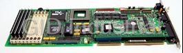
Intel CPUCP-S26361-D674 CPU Boards-486 CPU Board

Intel BOXD945GCLF Intel Atom processor 230 Intel 945GC Mini ITX Motherboard
Request a Quote

The quote request has been received
Close

Facing challenges or have inquiries? Feel free to contact us!
Call Us +1-469-283-2440
What they say about us
FANTASTIC RESOURCE
One of our top priorities is maintaining our business with precision, and we are constantly looking for affiliates that can help us achieve our goal. With the aid of GID Industrial, our obsolete product management has never been more efficient. They have been a great resource to our company, and have quickly become a go-to supplier on our list!
Bucher Emhart Glass
EXCELLENT SERVICE
With our strict fundamentals and high expectations, we were surprised when we came across GID Industrial and their competitive pricing. When we approached them with our issue, they were incredibly confident in being able to provide us with a seamless solution at the best price for us. GID Industrial quickly understood our needs and provided us with excellent service, as well as fully tested product to ensure what we received would be the right fit for our company.
Fuji
HARD TO FIND A BETTER PROVIDER
Our company provides services to aid in the manufacture of technological products, such as semiconductors and flat panel displays, and often searching for distributors of obsolete product we require can waste time and money. Finding GID Industrial proved to be a great asset to our company, with cost effective solutions and superior knowledge on all of their materials, it’d be hard to find a better provider of obsolete or hard to find products.
Applied Materials
CONSISTENTLY DELIVERS QUALITY SOLUTIONS
Over the years, the equipment used in our company becomes discontinued, but they’re still of great use to us and our customers. Once these products are no longer available through the manufacturer, finding a reliable, quick supplier is a necessity, and luckily for us, GID Industrial has provided the most trustworthy, quality solutions to our obsolete component needs.
Nidec Vamco
TERRIFIC RESOURCE
This company has been a terrific help to us (I work for Trican Well Service) in sourcing the Micron Ram Memory we needed for our Siemens computers. Great service! And great pricing! I know when the product is shipping and when it will arrive, all the way through the ordering process.
Trican Well Service
GO TO SOURCE
When I can't find an obsolete part, I first call GID and they'll come up with my parts every time. Great customer service and follow up as well. Scott emails me from time to time to touch base and see if we're having trouble finding something.....which is often with our 25 yr old equipment.
ConAgra Foods