

 Manufacturers
INTEL 75-SE7230NH1

Description
Intel 75-SE7230NH1 CPU Board
Part Number
75-SE7230NH1
Price
Request Quote
Manufacturer
INTEL
Lead Time
Request Quote
Category
PRODUCTS - 7
Specifications
Additional Connectors (Optional)
2 x Hi-Speed USB
BIOS Features
Multilingual BIOS, SMBIOS 2.3 support, Multiboot BBS 1.4 support
BIOS Type
AMI
Bus Clock
667 MHz, 400 MHz, 533 MHz
Cache Memory
None
Chipset Type
Intel E7230 / Intel ICH7R
Compatible Processors
Pentium 4, Pentium 4 Extreme Edition, Pentium D
Compliant Standards
RRL, BSMI, MIC, FCC, C-Tick, DOC, VCCI, UL, CB, EMC
Data Integrity Check
ECC
Depth
9.6 in
Expansion Slot(s)
2.0 x PCI PCI Express x8 / x4 ( 1.8 V ), 1.0 x DIMM 240-pin PCI Express x4 / x1, 4.0 x CPU, 1.0 x, 1.0 x
Graphics Controller
ATI ES1000
Interfaces
2.0 x USB 2.0, 2.0 x PS/2 mouse, 1.0 x LAN (Gigabit Ethernet), 1.0 x VGA, 1.0 x Serial, 1.0 x PS/2 keyboard
Internal Interfaces
1.0 x Floppy
Max Bus Speed
1066.0 MHz
Max Processors Qty
1.0
Max Size
8.0 GB
Modem
None
Network Interfaces
2 x Gigabit Ethernet
Packaged Quantity
1.0
Power Connectors
8-pin ATX12V connector, 24-pin main power connector
Processor
Intel Pentium D
Processor Socket
LGA775 Socket
Product Type
Motherboard - ATX
Registered or Buffered
Unbuffered
Speed
PC2-5300, PC2-4300, PC2-3200
Storage Interfaces
Intel ICH7R : ATA-100 - connector(s): 4 x 7pin Serial ATA - 4.0 device(s) - RAID 0 / RAID 1 / RAID 10, Serial ATA-300 - connector(s): 1 x 40pin IDC - 2.0 device(s)
Technology
DDR2 SDRAM
Video Memory
16.0 MB
Width
12.0 in
Features
- CPU Socket: Socket775
- Mainboard Chipset: E7230
- Mainboard Form Factor: ATX
- Mainboard Type: Servers
- Max Bus Speed: 1066MHz
- Pentium 4, Pentium 4 Extreme Edition, Pentium D
- RAM Max Supported Size: 8GB
Datasheet

Extracted Text
®
Intel Entry Server Board
SE7230NH1-E
Technical Product Specification
Revision 1.4
October 2006
Enterprise Platforms and Services Division
Revision History Intel® Entry Server Board SE7230NH1-E TPS
Revision History
Date Revision Modifications
Number
April 2005 0.5 Preliminary Release; subject to change.
July 2005 0.9 Updated BIOS Setup, connector designators, and jumpers.
October 1.2 Update, BIOS Setup and Network adapter information.
March 2006 1.3 Update, NIC LED, BIOS, Fan Control
October 2006 1.4 Update, SATA Transfer Rate, Riser operation MHz
ii Revision 1.4
Intel® Entry Server Board SE7230NH1-E TPS Disclaimers
Disclaimers
®
Information in this document is provided in connection with Intel products. No license, express
or implied, by estoppel or otherwise, to any intellectual property rights is granted by this
document. Except as provided in Intel's Terms and Conditions of Sale for such products, Intel
assumes no liability whatsoever, and Intel disclaims any express or implied warranty, relating to
sale and/or use of Intel products including liability or warranties relating to fitness for a particular
purpose, merchantability, or infringement of any patent, copyright or other intellectual property
right. Intel products are not intended for use in medical, life saving, or life sustaining
applications. Intel may make changes to specifications and product descriptions at any time,
without notice.
Designers must not rely on the absence or characteristics of any features or instructions marked
"reserved" or "undefined." Intel reserves these for future definition and shall have no
responsibility whatsoever for conflicts or incompatibilities arising from future changes to them.
This document contains information on products in the design phase of development. Do not
finalize a design with this information. Revised information will be published when the product is
available. Verify with your local sales office that you have the latest datasheet before finalizing a
design.
The Intel® Entry Server Board SE7230NH1-E may contain design defects or errors known as
errata which may cause the product to deviate from published specifications. Current
characterized errata are available on request.
This document and the software described in it is furnished under license and may only be used
or copied in accordance with the terms of the license. The information in this manual is
furnished for informational use only, is subject to change without notice, and should not be
construed as a commitment by Intel Corporation. Intel Corporation assumes no responsibility or
liability for any errors or inaccuracies that may appear in this document or any software that may
be provided in association with this document.
Except as permitted by such license, no part of this document may be reproduced, stored in a
retrieval system, or transmitted in any form or by any means without the express written consent
of Intel Corporation.
Intel, Pentium®, Itanium, and Xeon are trademarks or registered trademarks of Intel
Corporation.
*Other brands and names may be claimed as the property of others.
Copyright © Intel Corporation 2006.
iii
Revision 1.4
Table of Contents Intel® Entry Server Board SE7230NH1-E TPS
Table of Contents
1. Introduction ..........................................................................................................................1
1.1 Chapter Outline........................................................................................................1
1.2 Server Board Use Disclaimer ..................................................................................2
2. Server Board Overview........................................................................................................3
2.1 Intel® Entry Server Board SE7230NH1-E Feature Set ...........................................3
3. Functional Architecture .......................................................................................................9
3.1 Processor Sub-System ..........................................................................................10
3.1.1 Processor Voltage Regulator Down (VRD)............................................................11
3.1.2 Reset Configuration Logic .....................................................................................11
3.1.3 Processor Support .................................................................................................11
®
3.2 Intel E7230 Chipset..............................................................................................12
3.2.1 Memory Controller Hub (MCH) ..............................................................................12
3.2.2 PCI-X Hub (PXH)...................................................................................................16
3.2.3 I/O Controller Hub..................................................................................................16
3.3 Memory Sub-System .............................................................................................18
3.3.1 Memory Configuration ...........................................................................................19
3.3.2 Memory DIMM Support..........................................................................................21
3.4 I/O Sub-System .....................................................................................................21
3.4.1 PCI Subsystem ......................................................................................................21
3.4.2 Interrupt Routing ....................................................................................................23
3.5 PCI Error Handling.................................................................................................24
3.5.1 Video Support ........................................................................................................28
3.5.2 Network Interface Controller (NIC) ........................................................................29
3.5.3 Super I/O Chip .......................................................................................................30
3.5.4 BIOS Flash ............................................................................................................31
3.5.5 System Health Support..........................................................................................31
3.6 Replacing the Back-Up Battery..............................................................................33
4. System BIOS.......................................................................................................................34
4.1 BIOS Setup Utility ..................................................................................................34
4.1.1 Localization............................................................................................................34
4.1.2 Configuration Reset ...............................................................................................34
4.1.3 Keyboard Commands ............................................................................................34
iv Revision 1.4
Intel® Entry Server Board SE7230NH1-E TPS Table of Contents
4.1.4 Entering BIOS Setup .............................................................................................35
4.2 BIOS Updates........................................................................................................44
4.2.1 Preparing for the Upgrade .....................................................................................44
4.2.2 Recording the Current BIOS Settings....................................................................44
4.2.3 Obtaining the Upgrade Utility.................................................................................44
4.2.4 Creating a Bootable Diskette .................................................................................44
4.2.5 BIOS update instructions using iFlash utility..........................................................45
4.2.6 BIOS Update Instructions Using Express BIOS ....................................................45
4.2.7 Resetting CMOS After BIOS Update .....................................................................45
4.3 Operating System Boot, Sleep, and Wake ............................................................47
4.3.1 Advanced Configuration and Power Interface (ACPI) ...........................................47
5. Platform Management Architecture..................................................................................49
5.1 Reset Button ..........................................................................................................49
5.2 Diagnostic Interrupt Button (Control Panel NMI) ...................................................49
6. Error Reporting and Handling...........................................................................................50
6.1.1 BIOS Generated POST Error Beep Codes............................................................50
6.1.2 BIOS Event Log .....................................................................................................50
6.1.3 POST Code Checkpoints.......................................................................................52
6.1.4 Bootblock Initialization Code Checkpoints.............................................................54
6.1.5 Bootblock Recovery Code Checkpoint ..................................................................56
6.1.6 DIM Code Checkpoints..........................................................................................57
6.1.7 ACPI Runtime Checkpoints ...................................................................................57
6.2 Diagnostic LEDs ....................................................................................................57
6.2.1 Diagnostic LED POST Progress Codes ................................................................58
7. Connectors and Jumper Blocks .......................................................................................62
7.1 Power Connectors .................................................................................................62
7.1.1 Main Power Connector ..........................................................................................62
7.2 Intel Adaptive Slot..................................................................................................63
2
7.3 I C Header .............................................................................................................67
7.4 IDE Connector .......................................................................................................67
7.4.1 OEM RMC Connector............................................................................................68
7.5 Front Panel Connector...........................................................................................68
7.6 I/O Connectors.......................................................................................................69
7.6.1 VGA Connector......................................................................................................69
7.6.2 NIC Connectors .....................................................................................................69
v
Revision 1.4
Table of Contents Intel® Entry Server Board SE7230NH1-E TPS
7.6.3 ATA-100 Connector ...............................................................................................70
7.6.4 SATA Connectors ..................................................................................................70
7.6.5 Floppy Controller Connector..................................................................................70
7.6.6 Serial Port Connectors...........................................................................................71
7.6.7 Keyboard and Mouse Connector ...........................................................................71
7.6.8 USB Connector......................................................................................................72
7.7 Fan Headers ..........................................................................................................72
7.8 Miscellaneous Headers and Connectors ...............................................................73
7.8.1 Chassis Intrusion Header ......................................................................................73
7.8.2 Hard Drive Activity LED Header.............................................................................73
7.8.3 Back Panel I/O Connectors ...................................................................................74
7.8.4 System ID LED – LX SKU Only .............................................................................74
7.8.5 POST Code LEDs..................................................................................................74
7.9 Jumper Blocks .......................................................................................................74
7.9.1 Clear CMOS and System Maintenance Mode Jumpers ........................................74
8. Absolute Maximum Ratings ..............................................................................................76
8.1 Mean Time Between Failures (MTBF) Test Results..............................................76
9. Design and Environmental Specifications.......................................................................77
9.1 Intel® Entry Server Board SE7230NH1-E Power Budget......................................77
9.2 Power Supply Specifications .................................................................................77
9.2.1 Power Timing Requirements .................................................................................78
9.2.2 Dynamic Loading ...................................................................................................81
9.2.3 AC Line Transient Specification.............................................................................81
9.2.4 AC Line Fast Transient (EFT) Specification ..........................................................82
9.3 Product Regulatory Compliance ............................................................................82
9.3.1 Product Safety Compliance ...................................................................................82
9.3.2 Product EMC Compliance – Class A Compliance .................................................82
9.3.3 Certifications / Registrations / Declarations...........................................................83
9.3.4 Restrictions of Hazardous Substances (RoHS) Compliance.................................83
9.3.5 Product Regulatory Compliance Markings ............................................................84
9.4 Electromagnetic Compatibility Notices ..................................................................84
9.4.1 FCC (USA).............................................................................................................84
9.4.2 Industry Canada (ICES-003) .................................................................................85
9.4.3 Europe (CE Declaration of Conformity) .................................................................85
9.4.4 Taiwan Declaration of Conformity (BSMI)..............................................................86
vi Revision 1.4
Intel® Entry Server Board SE7230NH1-E TPS Table of Contents
9.4.5 Korean Compliance (RRL).....................................................................................86
9.4.6 Australia / New Zealand.........................................................................................86
9.5 Calculated Mean Time Between Failures (MTBF).................................................86
9.6 Mechanical Specifications .....................................................................................87
10. Hardware Monitoring .........................................................................................................90
10.1 Monitored Components .........................................................................................90
10.1.1 Fan Speed Control.................................................................................................91
10.1.2 Chassis Intrusion ...................................................................................................92
Glossary.....................................................................................................................................93
Reference Documents ..............................................................................................................96
vii
Revision 1.4
List of Figures Intel® Entry Server Board SE7230NH1-E TPS
List of Figures
Figure 1. Intel® Entry Server Board SE7230NH1-E (LX Version) Layout.....................................5
Figure 2. Intel® Entry Server Board SE7230NH1-E (LC SKU) Diagram ......................................7
Figure 3. Intel® Entry Server Board SE7230NH1-E Block Diagram.............................................9
Figure 4. Memory Bank Label Definition.....................................................................................20
Figure 5. Interrupt Routing Diagram ...........................................................................................26
Figure 6. Intel® ICH7R Interrupt Routing Diagram .....................................................................26
Figure 7. PXH-V Interrupt Routing Diagram ...............................................................................27
Figure 8. Back Panel I/O Connections (not to scale)..................................................................74
Figure 9. Output Voltage Timing .................................................................................................79
Figure 10. Turn On/Off Timing (Power Supply Signals)..............................................................80
®
Figure 11. Intel Entry Server Board SE7230NH1-E Mechanical Drawing.................................87
Figure 12. SKU 1 Pedestal Mount I/O Shield Mechanical Drawing ............................................88
Figure 13. SKU 2 Pedestal Mount I/O Shield Mechanical Drawing ............................................89
Figure 14. Fan Speed Control Block Diagram ............................................................................91
viii Revision 1.4
Intel® Entry Server Board SE7230NH1-E TPS List of Tables
List of Tables
Table 1. Server Board Layout Reference .....................................................................................6
Table 2. Server Board Layout Reference .....................................................................................8
Table 3. Processor Support Matrix .............................................................................................12
Table 4. Supported DDR2 Modules ............................................................................................14
Table 5. Segment B Configuration IDs .......................................................................................15
Table 6. Segment B Arbitration Connections..............................................................................15
Table 7. Segment D Configuration IDs .......................................................................................15
Table 8. Segment D Arbitration Connections..............................................................................16
Table 9. Segment E Connections ...............................................................................................16
Table 10. Memory Bank Labels and DIMM Population Order.....................................................20
Table 11. Characteristics of Dual/Single Channel Configuration with or without Dynamic Mode21
Table 12. PCI Bus Segment Characteristics...............................................................................22
Table 13. Segment A Configuration IDs .....................................................................................22
Table 14. Segment A Arbitration Connections.......................................................................23
Table 15. PCI AND PCI-X Interrupt Routing/Sharing..................................................................23
Table 16. Interrupt Definitions.....................................................................................................24
Table 17. Video Modes...............................................................................................................28
Table 18. Network Connector LED Status ..................................................................................29
Table 19. Intel® 82573E/V (NIC 1) .............................................................................................29
Table 20. Intel® 82541PI Gigabit Ethernet Controller (NIC 2)....................................................30
Table 21. Serial A Header Pin-out ..............................................................................................31
Table 22. BIOS Setup Keyboard Command Bar Options ...........................................................34
Table 23. BIOS Setup, Main Menu Options................................................................................36
Table 24. BIOS Setup, Additional System Information Sub-menu Selections ............................36
Table 25. BIOS Setup, Advanced Menu Options........................................................................37
Table 26. BIOS Setup, Advanced Menu, Boot Configuration Sub-menu Selections ..................38
Table 27. BIOS Setup, Advanced Menu, Peripheral Configuration Sub-menu...........................38
Table 28. BIOS Setup, Advanced Menu, Drive Configuration Menu Options.............................38
Table 29. BIOS Setup, Advanced Menu, Floppy Configuration Sub-menu Selections...............39
Table 30. BIOS Setup, Advanced Menu, Event Log Configuration Sub-menu Selections .........39
Table 31. BIOS Setup, Advanced Menu, Video Configuration Sub-menu Selections ................40
Table 32. BIOS Setup, Advanced Menu, Chipset Configuration Sub-menu Selections .............40
ix
Revision 1.4
List of Tables Intel® Entry Server Board SE7230NH1-E TPS
Table 33. BIOS Setup, Advanced Menu, Chipset Configuation, Memory Configuration Sub-
menu Selections...................................................................................................................41
Table 34. BIOS Setup, Advanced Menu, Chipset Configuation, PCI Express* Configuration Sub-
menu Selections...................................................................................................................41
Table 35. BIOS Setup, Advanced Menu, USB Mass Storage Device Configuration Sub-menu
Selections.............................................................................................................................41
Table 36. BIOS Setup, Security Menu Options...........................................................................42
Table 37. BIOS Setup, Power Menu Selections .........................................................................42
Table 38. BIOS Setup, Boot Menu Selections ............................................................................43
Table 39. BIOS Setup, Exit Menu Selections .............................................................................43
Table 40. Supported Wake Events .............................................................................................48
Table 41. BIOS Generated Beep Codes.....................................................................................50
Table 42. Troubleshooting BIOS Beep Codes............................................................................50
Table 43. POST Error Messages and Handling..........................................................................51
Table 44. POST Code Checkpoints............................................................................................52
Table 45. Bootblock Initialization Code Checkpoints..................................................................54
Table 46. Bootblock Recovery Code Checkpoint .......................................................................56
Table 47. DIM Code Checkpoints ...............................................................................................57
Table 48. ACPI Runtime Checkpoints ........................................................................................57
Table 49. POST Progress Code LED Example ..........................................................................58
Table 50. Boot Block POST Progress Codes .............................................................................58
Table 51. POST Progress Codes ...............................................................................................59
Table 52. Power Connector Pin-out (J6G1)................................................................................62
Table 53. Auxiliary CPU Power Connector Pin-out (J1B2) .........................................................62
Table 54. Intel Adaptive Slot Pin-Out (J6B2) ..............................................................................63
Table 55. HSBP Header Pin-out (J9E1) .....................................................................................67
Table 56. ATA 40-pin Connector Pin-out (J7J2) .........................................................................67
Table 57. RMC Header Pin-out (J9D1).......................................................................................68
Table 58. Front Panel 34-Pin Header Pin-out (J9J3)..................................................................68
Table 59. VGA Connector Pin-out (J2A1)...................................................................................69
Table 60. NIC1-Intel® 82541PI (10/100/1000) Connector Pin-out (J5A2)..................................69
Table 61. NIC2- Intel® 82573E/V (10/100/1000) Connector Pin-out (JA4A1) ............................69
Table 62. SATA Connector Pin-out (J9G2, J9H1, J9J2, J8J1) ...................................................70
Table 63. Legacy 34-pin Floppy Connector Pin-out (J7J3).........................................................70
Table 64. External DB9 Serial A Port Pin-out (J2A1)..................................................................71
Table 65. Keyboard and Mouse PS/2 Connectors Pin-out (J1A1)..............................................71
x Revision 1.4
Intel® Entry Server Board SE7230NH1-E TPS List of Tables
Table 66. USB Connectors Pin-out (J5A2) .................................................................................72
Table 67. Optional USB Connection Header Pin-out (J9F2) ......................................................72
Table 68. Three-pin Fan Headers Pin-out (Front J6J1, Rear J3B1) ...........................................72
Table 69. Four-pin Fan Headers Pin-out (Front J5J2, Rear J4B1, CPU J2D1) ..........................73
Table 70. Eight-pin Fan Header Pin-out (Right to Left – J5J1, J4J1, J4J3, J4J2) ......................73
Table 71. Intrusion Cable Connector (J9A1)Pin-Out ..................................................................73
Table 72. HDD LED Header (J1E1) Pin-Out...............................................................................74
Table 73. System Maintenance Mode (J9H3).............................................................................75
Table 74. Clear CMOS Jumper Options (J9G3) .........................................................................75
Table 75. Absolute Maximum Ratings ........................................................................................76
Table 76. The Board Power Budget............................................................................................77
Table 77. The Board Power Supply Voltage Specification .........................................................77
Table 78. Output Voltage Timing ................................................................................................78
Table 79. Turn On/Off Timing .....................................................................................................80
Table 80. Transient Load Requirements.....................................................................................81
Table 81. AC Line Sag Transient Performance ..........................................................................81
Table 82. AC Line Surge Transient Performance .......................................................................82
Table 83. Product Certification Markings....................................................................................84
Table 84. MTBF Data..................................................................................................................86
Table 85. Monitored Components...............................................................................................90
xi
Revision 1.4
List of Tables Intel® Entry Server Board SE7230NH1-E TPS
< This page intentionally left blank. >
xii Revision 1.4
Intel® Entry Server Board SE7230NH1-E TPS Introduction
1. Introduction
This Intel® Entry Server Board SE7230NH1-E Technical Product Specification (TPS) provides a
high-level technical description for the Intel® Entry Server Board SE7230NH1-E. It details the
architecture and feature set for all functional sub-systems that make up the server board.
1.1 Chapter Outline
This document is divided into the following chapters:
Chapter 1 – Introduction
Chapter 2 – Server Board Overview
Chapter 3 – Functional Architecture
Chapter 4 – System BIOS
Chapter 5 – Platform Management Architecture
Chapter 6 – Error Reporting and Handling
Chapter 7 – Connectors and Jumper Blocks
Chapter 8 – Absolute Maximum Ratings
Chapter 9 – Design and Environmental Specifications
Chapter 10 – Hardware Monitoring
Appendix A – Integration and Usage Tips
Glossary
Reference Documents
1
Revision 1.4
Introduction Intel® Entry Server Board SE7230NH1-E TPS
1.2 Server Board Use Disclaimer
Intel Corporation server baseboards contain a number of high-density VLSI* and power delivery
components that need adequate airflow to cool. Intel’s own chassis are designed and tested to
meet the intended thermal requirements of these components when the fully integrated system
is used together. It is the responsibility of the system integrator that chooses not to use Intel
developed server building blocks to consult vendor datasheets and operating parameters to
determine the amount of airflow required for their specific application and environmental
conditions. Intel Corporation cannot be held responsible if components fail or the server board
does not operate correctly when used outside any of its published operating or non-operating
limits.
2 Revision 1.4
Intel® Entry Server Board SE7230NH1-E TPS Server Board Overview
2. Server Board Overview
The Intel® Entry Server Board SE7230NH1-E is a monolithic printed circuit board with features
that is designed to support the entry server market.
2.1 Intel® Entry Server Board SE7230NH1-E Feature Set
The Intel® Entry Server Board SE7230NH1-E supports the following feature set:
Processor and Front Side Bus (FSB) support
- Supports Pentium® processor Extreme Edition, Pentium® D, Pentium® 4 and
Celeron® D processors in the Intel® LGA775 package
- Supports Intel® Dual Core Architecture
- Supports Hyper-Threading Technology
- Supports Intel® Extended Memory System 64 Technology (Intel® EM64T)
Intel® E7230 Chipset components
- Intel® E7230 MCH Memory Controller Hub
- Intel® ICH7R I/O Controller
- Intel® 6702 PXH-V-V PCI-X* Hub (LX SKU only)
- 12-deep In-order Queue
Memory System
Four DIMM sockets supporting 400/533/667MHz DDR2 DIMMs
Data bandwidth per channel of 4.2GB/s or 8.4GB/s in dual channel when using DDR2
667MHz
Support for up to two DDR2 channels for a total of four DIMMs (2 DIMMs / Channel)
providing up to 8GB max memory capacity.
Support for 256MB, 512MB, 1GB and 2GB DRAM modules
I/O Subsystem
LX Board I/O Subsystem (Five independent PCI Buses):
- Segment A: Two PCI 32-bit/33-MHz 3.3V Universal connectors supporting full length
PCI add-in cards (Adapters which support 5V only are not supported) and one
embedded Intel® 10/100/1000 82541PI Gigabit Ethernet Controller (Supports PCI
Specification, Rev 2.3)
- Segment B: One x1 PCI Express* resource implemented as an embedded Intel®
10/100/1000 82573E/V gigabit Ethernet Controller
- Segment C: One x1 PCI Express* resource implemented as a single x4 PCI
Express* connector supporting x1/x2/x4 PCI Express* add-in cards
- Segment D: One x4 PCI Express* resource supporting PXH-V-V PCI-X Hub. PXH-V-
V supports one dedicated PCI-X* 64/100MHz slot and PCI-X portion of Intel
Adaptive Slot
- Segment E: One x8 PCI Express* resource supporting PCI Express* portion of Intel
Adaptive Slot. Supports x1/x2/x4/x8 PCI Express* add-in cards via riser card
3
Revision 1.4
Server Board Overview Intel® Entry Server Board SE7230NH1-E TPS
LC Board I/O Subsystem (Five independent PCI Buses):
- Segment A: Two PCI 32-bit/33-MHz 3.3V Universal connectors supporting full length
PCI add-in cards (Adapters which support 5V only are not supported) and one
embedded Intel® 10/100/1000 82541PI Gigabit Ethernet Controller (Supports PCI
Specification, Rev 2.3)
- Segment B: One x1 PCI Express* resource implemented as an embedded Intel®
10/100/1000 82573E/V gigabit Ethernet Controller
- Segment C: One x1 PCI Express* resource implemented as a single x4 PCI
Express* connector supporting x1/x2/x4 PCI Express* add-in cards
- Segment D: One x4 PCI Express* resource implemented as a single x8 PCI
Express* connector supporting x1/x2/x4/x8 PCI Express* add-in cards
- Segment E: One x8 PCI Express* resource implemented as a single x8 PCI
Express* connector supporting x1/x2/x4/x8 PCI Express* add-in cards
Serial ATA host controller
Four independent SATA ports support data transfer rates up to 3.0 Gb/s (300MB/s) per
port
IDE controller
- One IDE connector, supporting a maximum of two ATA-100* compatible devices
Universal Serial Bus 2.0 (USB)
Two external USB ports with an additional internal header providing two optional USB
ports for front panel support.
- Supports wake-up from sleeping states S1-S4 (S3 not supported)
- Supports Legacy Keyboard/Mouse connections when using PS2-USB dongle
LPC (Low Pin Count) bus segment with one embedded device
- Super I/O controller chips providing all PC-compatible I/O (floppy, serial, keyboard,
mouse, two serial com port ) and integrated hardware monitoring
- LC Super I/O = SMsC* LP47M182NR
- LX Super I/O = National Semiconductor* PC8374LOIBU
SSI-compliant connectors for SSI interface support
Standard Intel 34pin SSI front panel and 2x12 and 2x4 power connectors
Fan Support
Fans:
- Two general purpose 3-pin fans
- Two general purpose 4-pin fans
- One 4-pin processor fan (active heatsink required)
- Four 8-pin dual rotor fans for Intel High Density applications (Intel® Server Chassis
SC1475 and Intel® Server Platform SR1474NH1-E).
Diagnostic LEDs to display POST code indicators during boot
4 Revision 1.4
Intel® Entry Server Board SE7230NH1-E TPS Server Board Overview
The following figure shows the board layout of the Intel® Entry Server Board SE7230NH1-E (LX
version). Each connector and major component is identified by letter and is identified in Table 2.
A C E G I K
L
B D F H J
M
N
O
P
VV
UU
TT
SS
RR
QQ
PP
OO
MM KK II GG EE CC AA X V T R
JJ BB Z W U S Q
NN LL HH FF DD
Y
Figure 1. Intel® Entry Server Board SE7230NH1-E (LX Version) Layout
5
Revision 1.4
Server Board Overview Intel® Entry Server Board SE7230NH1-E TPS
Table 1. Server Board Layout Reference
Ref Description Ref Description Ref Description
A Chassis Intrusion Header Q Memory Slot DIMM 2B GG Floppy Connector
B PCI (32bit/33MHz) Slot 1 R Memory Slot DIMM 1B HH SCSI LED Connector (moved)
C PCI (32bit/33MHz) Slot 2 S Memory Slot DIMM 2A II National* PC8374L0IBU SIO
D ATI ES1000 Video Controller T Memory Slot DIMM 1A JJ SATA Port 3
E PCI Express* x4 (x1 Lane) Slot 3 U 775 Land (LGA) CPU Socket KK SATA Port 2
® ®
F PCI Express* x8 (x4 Lane) Slot 4 V Intel 7230 MCH LL Intel 82802 ICH7R
G Intel® 82541PI LAN Controller W SysFan8 MM Clear CMOS Jumper
H PCI-X* (64bit/133MHz) Slot 5 X SysFan7 NN Maintenance Mode Jumper
I LAN SPI Flash Y Hardware Management Controller OO Front Panel Connector
J Intel® 82573E/V LAN Controller Z SysFan6 PP SATA Port 1
K Intel® Adaptive Slot, Slot 6 AA SysFan5 QQ SATA Port 0
L Back Panel Connectors BB SysFan4 RR External USB Connector
M SysFan1 CC Hardware Management Controller SS BIOS SPI Flash
N SysFan2 DD 2 x 12 Power Connector TT Intel® 6702 PXH-V-V
Controller
2
O 2 x 4 Power Connector EE SysFan3 UU I C Connector
P CPU Fan FF PATA IDE Connector VV RMC Connector
WW NIC1 FW Enable
6 Revision 1.4
Intel® Entry Server Board SE7230NH1-E TPS Server Board Overview
The following figure shows the board layout of the Intel® Entry Server Board SE7230NH1-E (LC
SKU version). Each connector and major component is identified by letter and is identified in
Table 2.
A C E G H
J
K
B D F I
L
M
N
O
PP
OO
NN
MM
LL
KK
JJ
HH FF BB Z X U
DD S Q
T R P
II GG EE CC AA Y W
V
Figure 2. Intel® Entry Server Board SE7230NH1-E (LC SKU) Diagram
7
Revision 1.4
Server Board Overview Intel® Entry Server Board SE7230NH1-E TPS
Table 2. Server Board Layout Reference
Ref Description Ref Description Ref Description
A Chassis Intrusion Header O CPU Fan CC SCSI LED Connector (moved)
B PCI (32bit/33MHz) Slot 1 P Memory Slot DIMM 2B DD SMsC LPC47M182NR SIO
C PCI (32bit/33MHz) Slot 2 Q Memory Slot DIMM 1B EE SATA Port 3
D ATI ES1000 Video Controller R Memory Slot DIMM 2A FF SATA Port 2
®
E PCI Express* x4 (x1 Lane) Slot 3 S Memory Slot DIMM 1A GG Intel 82802 ICH7R
F PCI Express* x8 (x4 Lane) Slot 4 T 775 Land (LGA) CPU Socket HH Clear CMOS Jumper
®
G Intel® 82541PI LAN Controller U Intel 7230 MCH II Maintenance Mode Jumper
H LAN SPI Flash V Hardware Management Controller JJ Front Panel Connector
I Intel® 82573E/V LAN Controller W SysFan4 KK SATA Port 1
J PCI Express* x8 (x8 Lane) Slot 6 X Hardware Management Controller LL SATA Port 0
K Back Panel Connectors Y 2 x 12 Power Connector MM External USB Connector
L SysFan1 Z SysFan3 NN BIOS SPI Flash
2
M SysFan2 AA PATA IDE Connector OO I C Connector
N 2 x 4 Power Connector BB Floppy Connector PP RMC Connector
8 Revision 1.4
Intel® Entry Server Board SE7230NH1-E TPS Functional Architecture
3. Functional Architecture
This chapter provides a high-level description of the functionality associated with the
architectural blocks that make up the Intel® Entry Server Board SE7230NH1-E.
Figure 3. Intel® Entry Server Board SE7230NH1-E Block Diagram
9
Revision 1.4
Functional Architecture Intel® Entry Server Board SE7230NH1-E TPS
3.1 Processor Sub-System
The Intel® Entry Server Board SE7230NH1-E supports the following:
Pentium® processor Extreme Edition in the 775-land package
Pentium® D processors in the 775-land package
Pentium® 4 processors in the 775-land package
Celeron® D processors in the 775-land package
The 775-land package is a follow on to Pentium® 4 and Celeron® processors in the 478-pin
package with enhancements to the Intel® NetBurst® micro-architecture including but not limited
to the following:
Dual Core Architecture
Hyper-Threading Technology
Intel® EM64T
Pentium® processor Extreme Edition
Pentium® D
Pentium® 4
Celeron® D
The processors built on 90nm and 65nm process technology in the 775-land package utilize
Flip-Chip Land Grid Array (FC-LGA4) package technology, and plug into a 775-land LGA
®
socket, referred to as the Intel LGA775 socket. The processors are as follows:
Pentium® processor Extreme Edition
Pentium® D Processor
Pentium® 4 Processor
Celeron® D Processor
The above processors in the 775-land package, like their predecessors in the 478-pin package,
is based on the same Pentium® 4 micro-architecture. They maintain compatibility with 32-bit
software written for the IA-32 instruction set, while supporting 64-bit native mode operation
when coupled with supported 64-bit operating systems and applications.
The Celeron® Processor currently does not come in a dual core configuration, support Hyper-
Threading Technology or Intel® EM64T.
10 Revision 1.4
Intel® Entry Server Board SE7230NH1-E TPS Functional Architecture
3.1.1 Processor Voltage Regulator Down (VRD)
The Intel® Entry Server Board SE7230NH1-E has a VRD (Voltage Regulator Down) to support
one processor. It is compliant with the VRM 10.1 DC-DC Converter Design Guide Line and
provides a maximum of 120A, which is capable of supporting the requirements for the following
processors:
Pentium® processor Extreme Edition
Pentium® D Processor
Pentium® 4 Processor
Celeron® D Processor
The board hardware monitors the processor VTTEN (Output enable for VTT) pin before turning
on the VRD. If the VTTEN pin of the processors is not identical, the Power ON Logic will not turn
on the VRD.
3.1.2 Reset Configuration Logic
The BIOS determines the processor stepping, cache size, et cetera through the CPUID
instruction. The requirements are as follows:
Processors run at a fixed speed, but can be programmed by BIOS to operate at a lower
or higher speed.
The processor information is read at every system power-on.
Note: The processor speed is the processor power-on reset default value. No manual processor
speed setting options exist either in the form of a BIOS setup option or jumpers.
3.1.3 Processor Support
®
The Intel® Entry Server Board SE7230NH1-E supports one processor in the Intel LGA775
package. The support circuitry on the server board consists of the following:
®
Intel LGA775 processor socket supporting:
- 800MHz Pentium® D Processor
- Pentium® 4 Processor
- 1066MHz FSB Pentium® processor Extreme Edition
- Pentium® processor Extreme Edition
Processor host bus AGTL+ support circuitry.
11
Revision 1.4
Functional Architecture Intel® Entry Server Board SE7230NH1-E TPS
Table 3. Processor Support Matrix
Processor Family Package Type Frequency Cache Size Front Side Bus
®
Pentium 4 processor ®
Intel LGA775 3.2GHz 2 x 1MB L2 800MHz
Extreme Edition
®
Pentium 4 processor ®
Intel LGA775 3.73GHz 2MB L2 1066MHz
Extreme Edition
®
Pentium® D Intel LGA775 3.2 – 4.0GHz 2 x 1MB L2 800MHz
®
Pentium® 4 Intel LGA775 3.2 – 4.0GHz 1MB or 2MB L2 800MHz
®
Celeron® D Intel LGA775 2.26 – 3.2 GHz 256K L2 533MHz
Note: For a complete list of all supported processors, please visit the Intel® Entry Server Board
SE7230NH1-E support site located at the following URL:
http://support.intel.com/support/motherboards/server/sb/CS-012690.htm
In addition to the circuitry described above, the processor subsystem contains the following:
Reset configuration logic
Server management registers and sensors
®
3.2 Intel E7230 Chipset
The Intel® Entry Server Board SE7230NH1-E is designed around the Intel® E7230 Chipset.
The chipset provides an integrated I/O bridge and memory controller, and a flexible I/O
subsystem core (PCI Express*). The chipset consists of three primary components:
3.2.1 Memory Controller Hub (MCH)
3.2.1.1 Intel® E7230 Chipset MCH: Memory Control Hub
The MCH accepts access requests from the host (processor) bus and directs those accesses to
memory or to one of the PCI buses. The MCH monitors the host bus, examining addresses for
each request. Accesses may be directed to the following:
A memory request queue for subsequent forwarding to the memory subsystem
An outbound request queue for subsequent forwarding to one of the PCI buses
The MCH also accepts inbound requests from the Intel® ICH7R. The MCH is responsible for
generating the appropriate controls to control data transfer to and from memory.
12 Revision 1.4
Intel® Entry Server Board SE7230NH1-E TPS Functional Architecture
The MCH is a 1210-ball FC-BGA device and uses the proven components of the following
previous generations:
Pentium® processor Extreme Edition
Pentium® D Processor
Pentium® 4 Processor bus interface unit
Hub interface unit
DDR2 memory interface unit
In addition, the MCH incorporates an integrated high performance graphics media accelerator
and a PCI Express* interface. The PCI Express* interface allows the MCH to directly interface
with the PCI Express* devices (like PXH-V/PXH-VD). The MCH also increases the main
memory interface bandwidth and maximum memory configuration with a 72-bit wide memory
interface.
The MCH integrates the following main functions:
An integrated high performance main memory subsystem
A PCI Express* bus which provides an interface to the PCI-Express devices( Fully
compliant to the PCI Express* Base Specification, Rev 1.0a)
A DMI which provides an interface to the Intel® ICH7R
Other features provided by the MCH include the following:
Full support of ECC on the processor bus
Full support of Intel® x4 Single Device Data Correction on the memory interface with x4
DIMMs
Twelve deep in-order queue, two deep defer queue
Full support of un-buffered DDR2 ECC DIMMs
Support for 256MB, 512MB, 1 GB and 2 GB DDR2 memory modules
Memory scrubbing
3.2.1.2 MCH Memory Sub-System Overview
The MCH supports a 72-bit wide memory sub-system that can support a maximum of 8 GB of
DDR2 memory using two GB DIMMs. This configuration needs external registers for buffering
the memory address and control signals. The four chip selects are registered inside the MCH
and need no external registers for chip selects.
The memory interface runs at 400/533/667MT/s. The memory interface supports a 72-bit wide
memory array. It uses seventeen address lines (BA [2:0] and MA [13:0]) and supports 256 MB,
512 MB, 1 GB, and 2GB DRAM densities. The DDR DIMM interface supports memory
scrubbing, single-bit error correction, and multiple bit error detection and Intel® x4 Single
Device Data Correction with x4 DIMMs.
13
Revision 1.4
Functional Architecture Intel® Entry Server Board SE7230NH1-E TPS
3.2.1.2.1 DDR2 Configurations
The DDR2 interface supports up to 8 GB of main memory and supports single- and double-
density DIMMs. The DDR2 can be any industry-standard DDR2. The following table shows the
DDR2 DIMM technology supported.
Table 4. Supported DDR2 Modules
DDR2-400/533/667 Un-buffered
SDRAM Module Matrix
DIMM DIMM SDRAM SDRAM # SDRAM # Address bits
Capacity Organization Density Organization Devices/rows/Banks rows/Banks/column
256MB 32M x 72 256Mbit 32M x 8 9 /1 / 4 13 / 2 / 10
512MB 64M x 72 256Mbit 32M x 8 18 / 2 / 4 13 / 2 / 10
512MB 64M x 72 512Mbit 64M x 8 9 / 1 / 4 14 / 2 / 10
1GB 128M x 72 512Mbit 64M x 8 18 / 2 / 4 14 / 2 / 10
1GB 128M x 72 1Gbit 128M x 8 9 / 1 / 8 14 / 4 / 10
2GB 256M x 72 2GB 128M x 8 18 / 2 / 8 14 / 8 / 10
3.2.1.3 PCI Express*
3.2.1.3.1 x4 PCI Express* Subsystem
The Intel® ICH7R supports one x4-lane PCI Express* interface that can also be configured as a
single x1 or x4-lane port. The PCI Express* interface allows direct connection with the PXH-V-V
or dedicated PCI-E devices. (Fully compliant to the PCI Express* Base Specification, Rev 1.0a).
3.2.1.3.2 x1 PCI Express* Subsystem
The Intel® ICH7R supports 2 x1 PCI Express* buses. One supports a dedicated x4 PCI
Express* slot. The other supports the Intel® 82573-gigabit Ethernet controller.
One 32-bit PCI bus segment is directed through the Intel® ICH7R Interface A. This PCI
Segment B only has an embedded device, Intel® 82573E/V LAN (NIC2) clocked at 1.5GHz.
3.2.1.3.2.1 Device IDs (IDSEL)
Each device under the PCI hub bridge has its IDSEL signal connected to one bit of AD [31:16],
which acts as a chip select on the PCI bus segment in configuration cycles. This determines a
unique PCI device ID value for use in configuration cycles. The following table shows the bit to
which each IDSEL signal is attached for P32-B devices and corresponding device description:
14 Revision 1.4
Intel® Entry Server Board SE7230NH1-E TPS Functional Architecture
Table 5. Segment B Configuration IDs
IDSEL Value Device
19 Intel® 82573E/V LAN (NIC2)
3.2.1.3.2.2 Segment B Arbitration
PCI Segment B supports one PCI masters. All PCI masters must arbitrate for PCI access using
resources supplied by the Intel® ICH7R. The host bridge PCI interface arbitration lines REQx*
and GNTx* are internal to the Intel® ICH7R. The following table defines the arbitration
connections:
Table 6. Segment B Arbitration Connections
Baseboard Signals Device
PCIX REQ_N0/GNT_N0 Intel® 82541PI LAN (NIC2)
3.2.1.3.2.3 Segment D 64bit/133MHz PCI-X Subsystem
One 64-bit PCI-X* bus segment is directed through the PXH-V. This PCI-X* segment, Segment
D interface A, provides the following:
Two 3.3V 64-bit PCI-X* slots or
One 3.3V 64-bit PCI-X* riser slot, (Intel® Entry Server Board SE7230NH1LX SKU only)
The PCI-X* slot is capable of speeds up to 133MHz operation and supports full-length PCI and
PCI-X adapters. If installed, the riser forces the slot to operate at 100MHz.
3.2.1.3.2.3.1 Device IDs (IDSEL)
Each device under the PCI hub bridge has its IDSEL signal connected to one bit of AD [31:16],
which acts as a chip select on the PCI bus segment in configuration cycles. This determines a
unique PCI device ID value for use in configuration cycles. The following table shows the bit to
which each IDSEL signal is attached for P64-C devices and corresponding device description:
Table 7. Segment D Configuration IDs
IDSEL Value Device
17 PCI Slot 5 (64bit/66-133MHz) (Intel® Entry Server Board SE7230NH1LX SKU only)
18 PCI Slot 6 (64bit/133MHz) (Riser, Intel® Entry Server Board SE7230NH1LX SKU only)
15
Revision 1.4
Functional Architecture Intel® Entry Server Board SE7230NH1-E TPS
3.2.1.3.2.3.2 Segment D Arbitration
P64-C supports two PCI masters: two PCI-X slots or one riser slot. All PCI masters must
arbitrate for PCI access using resources supplied by the ICH7. The host bridge PCI interface
(ICH7) arbitration lines REQx* and GNTx* are a special case in that they are internal to the host
bridge. The following table defines the arbitration connections.
Table 8. Segment D Arbitration Connections
Baseboard Signals Device
PCIX REQ_N0/GNT_N0 PCI Slot 5 (64bit/133MHz) (Intel® Entry Server Board SE7230NH1LX SKU only)
PCI Slot 6 (64bit/133MHz) (Riser, Intel® Entry Server Board SE7230NH1LX SKU
PCIX REQ_N1/GNT_N1
only)
3.2.1.3.2.3.3 Segment E PCI-E x8
In this board, Lanes 0~7 are connected to an x8 PCI-E connector directly through the MCH. It
can support x1, x4, x 8 PCI-E add-in cards or through the I/O riser through the Intel® Adaptive
Slot (LX SKU only)
Table 9. Segment E Connections
Lane Device
Lane 0~7 Slot 6 or Intel® Adaptive Slot (PCI Express* x8)
3.2.2 PCI-X Hub (PXH)
PXH-V-V: PCI-X Hub (LX SKU Only) The PXH-V hub is a peripheral chip that performs PCI
bridging functions between the PCI Express* interface and the PCI bus. The PXH-V contains
two PCI bus interfaces that can be independently configured to operate in PCI (33 or 66 MHz),
PCI-X Mode1 (66,100,133), for either 32 or 64 bits.
3.2.3 I/O Controller Hub
3.2.3.1 Intel® ICH7R: I/O Controller Hub 7R
The Intel® ICH7R controller has several components. It provides the interface for a 32-bit/33-
MHz PCI bus. The Intel® ICH7R can be both a master and a target on that PCI bus. The Intel®
ICH7R also includes a USB 2.0 controller and an IDE controller. The Intel® ICH7R is also
responsible for much of the power management functions, with ACPI control registers built in.
The Intel® ICH7R also provides a number of GPIO pins and has the LPC bus to support low
speed Legacy I/O.
The MCH and Intel® ICH7R chips provide the pathway between the processor and the I/O
systems. The MCH is responsible for accepting access requests from the host (processor) bus,
and directing all I/O accesses to one of the PCI buses or Legacy I/O locations. If the cycle is
directed to one of the PCI-E segments, the MCH communicates with the PCI-E Devices (add-in
16 Revision 1.4
Intel® Entry Server Board SE7230NH1-E TPS Functional Architecture
card, on board devices) through the PCI-E interface. If the cycle is directed to the Intel® ICH7R,
the cycle is output on the MCH’s DMI bus. All I/O for the board, including PCI and PC-
compatible I/O, is directed through the MCH and then through the Intel® ICH7R provided PCI
buses.
The Intel® ICH7R is a multi-function device, housed in a 609-pin mBGA device. It provides the
following:
A DMI bus
A PCI 32-bit/33 MHz interface
An IDE interface
An integrated Serial ATA Host controller
A USB controller
A PCI-E x4 interface
A power management controller
Each function within the Intel® ICH7R has its own set of configuration registers. Once
configured, each appears to the system as a distinct hardware controller sharing the same PCI
bus interface.
The primary role of the ICH7R is providing the gateway to all PC-compatible I/O devices and
features. The board uses the following the Intel® ICH7R features:
PCI 32-bit/33MHz interface for PCI slots 1 and 2 and Intel® 82541PI Gigabit Ethernet
Controller
PCI 32-bit/33MHz interface to dedicated ATI ES1000* video subsystem
LPC bus interface
x4 PCI Express* interface for PXH-V-V device (supplies PCI-X on LX SKU only)
x1 PCI Express* resource for dedicated x4 PCI Express* slot
x1 PCI Express* interface for Intel® 82573E/V gigabit Ethernet Controller
DMI (Direct Media Interface)
IDE interface, with Ultra ATA 100/66/33 capability
Integrated quad-port Serial ATA Host controller
Universal Serial Bus (USB) 2.0 interface
PC-compatible timer/counter and DMA controllers
APIC and 82C59 interrupt controller
Power management
System RTC
Supports Smbus 2.0 Specification
General purpose I/O (GPIO)
The following are the descriptions of how each supported feature is used for Intel® ICH7R on
the board.
17
Revision 1.4
Functional Architecture Intel® Entry Server Board SE7230NH1-E TPS
3.2.3.2 IDE Interface (Bus Master Capability and Synchronous DMA Mode)
The Intel® ICH7R acts as a PCI-based Ultra ATA 100/66/33 IDE controller that supports
programmed I/O transfers and bus master IDE transfers. The Intel® ICH7R supports one IDE
channel, supporting two drives each (drives 0 and 1). The baseboard provides a 40-pin (2x20)
IDE connector to access the IDE functionality.
The IDE interface supports Ultra ATA 100/66/33 Synchronous DMA Mode transfers on the 40-
pin connector.
3.2.3.3 SATA Controller
The Intel® ICH7R contains four SATA ports. The data transfer rates up to 300Mbyte/s per port.
3.2.3.4 Compatibility Modules (DMA Controller, Timer/Counters, Interrupt
Controller)
The Intel® ICH7R provides the functionality of two-cascaded 82C59 with 15 interrupts handling.
Support processor system bus interrupt.
3.2.3.5 Advanced Programmable Interrupt Controller (APIC)
Interrupt generation and notification to the processor is done by the APICs in the Intel® ICH7R
using messages on the front side bus.
3.2.3.6 Universal Serial Bus (USB) Controller
The Intel® ICH7R contains one EHCI USB 2.0 controller and four USB ports. The USB
controller moves data between main memory and up to four USB connectors. All ports function
identically and with the same bandwidth. The Intel® Server Board SE7230NH1-E implements
four ports on the board.
The baseboard provides two external USB ports on the back of the server board. The dual-stack
USB connector is located within the standard ATX I/O panel area. The Universal Serial Bus
Specification, Revision 1.1, defines the external connectors.
The third/fourth USB port is optional and can be accessed by cabling from an internal 9-pin
connector located on the base board to an external USB port located either in front or the rear
of a given chassis.
3.2.3.7 Enhanced Power Management
One of the embedded functions of the Intel® ICH7R is a power management controller. This is
used to implement ACPI-compliant power management features. The baseboard does support
sleep states S1, S4, and S5.
3.3 Memory Sub-System
The baseboard supports up to four DIMM slots for a maximum memory capacity of 8 GB. The
DIMM organization is x72, which includes eight ECC check bits. The memory interface runs at
400/533/667MTs. The memory controller supports the following:
18 Revision 1.4
Intel® Entry Server Board SE7230NH1-E TPS Functional Architecture
Memory scrubbing
Single-bit error correction
Multiple-bit error detection
Intel® x4 Single Device Data Correction support with x4 DIMMs
Memory can be implemented with either single sided (one row) or double-sided (two row)
DIMMs
3.3.1 Memory Configuration
The memory interface between the MCH and the DIMMs is 64-bit (non-ECC) or 72-bit (ECC)
wide interface.
There are two banks of DIMMs, labeled 1 and 2. Bank 1 contains DIMM socket locations
DIMM_1A and DIMM_2A. Bank 2 contains DIMM socket locations DIMM_1B and DIMM_2B.
The sockets associated with each bank or “channel,” are located next to each other and the
DIMM socket identifiers are marked on the base board silkscreen, near the DIMM socket. Bank
1 is associated with Memory Channel A while Bank 2 is associated with Memory Channel B.
When only two DIMM modules are being used, the population order must be DIMM_1A,
DIMM_1B to ensure dual channel operating mode.
In order to operate in dual channel dynamic paging mode, the following conditions must
be met:
Two identical DIMMs are installed, one each in DIMM_1A and DIMM_1B
Four identical DIMMs are installed (one in each socket location)
Note: Installing only three DIMMs is not supported. Do not use DIMMs that are not “matched” (same
type and speed). Use of identical memory parts is always the preferred method.
See Figure 4 on the following page for reference.
The system design is free to populate or not to populate any rank on either channel, including
either degenerate single channel case.
DIMM and memory configurations must adhere to the following:
DDR2 400/533/667 , un-buffered, DDR2 DIMM modules
DIMM organization: x72 ECC or x 64 Non-ECC
Pin count: 240
DIMM capacity: 256 MB, 512 MB, 1 GB and 2 GB DIMMs
Serial PD: JEDEC Rev 2.0
Voltage options: 1.8 V
Interface: SSTL2
19
Revision 1.4
Functional Architecture Intel® Entry Server Board SE7230NH1-E TPS
Table 10. Memory Bank Labels and DIMM Population Order
Location DIMM Label Channel Population Order
J2J1 (DIMM_1A) A 1
J2J2 (DIMM_2A) A 3
J1J1 (DIMM_1B) B 2
J1J2 (DIMM_2B) B 4
Figure 4. Memory Bank Label Definition
20 Revision 1.4
Intel® Entry Server Board SE7230NH1-E TPS Functional Architecture
Table 11. Characteristics of Dual/Single Channel Configuration with or without Dynamic Mode
Throughput Level Configuration Characteristics
Highest Dual channel with dynamic paging mode All DIMMs matched
Dual channel without dynamic paging mode DIMMs matched from Channel A to Channel B
DIMMs not matched within channels
Single channel with dynamic paging mode Single DIMM or DIMMs matched with a
channel
Lowest Single channel without dynamic paging DIMMs not matched
mode
3.3.2 Memory DIMM Support
The board supports un-buffered (not registered) DDR2 400/533/667 ECC or Non-ECC DIMMs
operating at 400/533/667MT/s. Only DIMMs tested and qualified by Intel or a designated
memory test vendor are supported on this board. A list of qualified DIMMs is available at
http://support.intel.com/support/motherboards/server/SE7230NH1E. Note that all DIMMs are
supported by design, but only fully qualified DIMMs will be supported on the board.
The minimum supported DIMM size is 256 MB. Therefore, the minimum main memory
configuration is 1 x 256 MB or 256 MB. The largest size DIMM supported is 2 GB and as such,
the maximum main memory configuration is 8 GB implemented by 4 x 2 GB DIMMs.
Only un-buffered DDR2 400/533/667 compliant, ECC x8 and Non-ECC x8 or x16
memory DIMMs are supported.
ECC single-bit errors (SBE) will be corrected while multiple-bit error (MBE) will only be
detected.
Intel® Entry Server Board SE7230NH1-E also supports Intel® x4 Single Device Data
Correction with x4 DIMMs.
The maximum memory capacity is 8 GB via four 2 GB DIMM modules.
The minimum memory capacity is 256 MB via a single 256 MB DIMM module.
3.4 I/O Sub-System
3.4.1 PCI Subsystem
The primary I/O buses for the Intel® Entry Server Board SE7230NH1-E are five independent
PCI bus segments providing PCI, PCI-E and PCI-X* resources (LX SKU only). The PCI buses
comply with the PCI Local Bus Specification, Rev 2.3.
PCI Segments A, B and C are directed through the Intel® ICH7R. PCI Segment D is
independently configured to PXH-V that is through Intel® ICH7R by PCI Express* x4 interface.
PCI Segment E is directed through the MCH by PCI-E x8 interface. The table below lists the
characteristics of the three PCI bus segments.
21
Revision 1.4
Functional Architecture Intel® Entry Server Board SE7230NH1-E TPS
Table 12. PCI Bus Segment Characteristics
PCI Bus
Voltage Width Speed Type PCI I/O Card Slots
Segment
A 3.3V 32 bits 33MHz PCI 32 Slot 1, Slot 2, NIC 1
B 3.3V 1 lane 1.5GHz x1 PCI-E NIC 2
C 3.3V 1 lane 1.5GHz x1 PCI-E Slot 3
D 3.3V 4 lanes 1.5GHz x4 PCI-E Slot 4
D 3.3V 64 bits 66/100/133MHz PCI-64 Slot 5; (Slot 6 through riser card)
E 3.3V 8 lanes 1.5GHz x8 PCI-E Slot 6
3.4.1.1 P32-A: 32-bit, 33-MHz PCI Subsystem
The Intel® ICH7R provides a Legacy 32-bit PCI subsystem and acts as the central resource on
this PCI interface. P32-A supports the following embedded devices and connectors:
One Intel® 82541PI Network Controller
Two slots capable of supporting full length PCI add-in cards operating at 33 MHz
All 32-bit/33-MHz PCI I/O for the board is directed through the Intel® ICH7R. The 32-bit/33-MHz
PCI segment created by the Intel® ICH7R is known as PCI Segment A. Segment A supports the
following embedded devices and connectors:
One 10/100/1000-T Network Interface Controller: Intel® 82541PI Fast Ethernet
Controller.
3.4.1.1.1 Device IDs (IDSEL)
Each device under the PCI hub bridge has its IDSEL signal connected to one bit of AD (31:16),
which acts as a chip select on the PCI bus segment in configuration cycles. This determines a
unique PCI device ID value for use in configuration cycles. The following table shows the bit to
which each IDSEL signal is attached for Segment A devices and the corresponding device
description.
Table 13. Segment A Configuration IDs
IDSEL Value Device
19 Intel® 82541PI LAN (NIC2)
18 PCI Slot 1 and 2 (32b/33MHz)
3.4.1.1.2 Segment A Arbitration
PCI Segment A supports two PCI devices: the Intel® ICH7R and one PCI bus masters (NIC). All
PCI masters must arbitrate for PCI access, using resources supplied by the Intel® ICH7R. The
host bridge PCI interface (ICH7R) arbitration lines REQx* and GNTx* are a special case in that
they are internal to the host bridge. The following table defines the arbitration connections.
22 Revision 1.4
Intel® Entry Server Board SE7230NH1-E TPS Functional Architecture
Table 14. Segment A Arbitration Connections
Baseboard Signals Device
PCI REQ1_N/GNT_N1 Intel® 82541PI LAN (NIC1)
PCI REQ0_N/GNT_N0 PCI Slot 1 and 2 (32bit/33MHz)
3.4.1.2 PCI Interface for ATI Video subsystem
The server board graphics subsystem is connected to the Intel® ICH7R via a 32/33MHz PCI
bus.
3.4.2 Interrupt Routing
The board interrupt architecture accommodates both PC-compatible PIC mode and APIC mode
interrupts through use of the integrated I/O APICs in the ICH7.
3.4.2.1 Legacy Interrupt Routing
For PC-compatible mode, the ICH7 provides two 82C59-compatible interrupt controllers. The
two controllers are cascaded with interrupt levels 8-15 entering on level 2 of the primary
interrupt controller (standard PC configuration). A single interrupt signal is presented to the
processors, to which only one processor will respond for servicing. The Intel® ICH7R contains
configuration registers that define which interrupt source logically maps to I/O APIC INTx pins.
The ICH7 handles both PCI and IRQ interrupts. The Intel® ICH7R translates these to the APIC
bus. The numbers in the table below indicate the Intel® ICH7R PCI interrupt input pin to which
the associated device interrupt (INTA, INTB, INTC, INTD, INTE, INTF, INTG, INTH for PCI bus
and PXIRQ0, PXIRQ1, PXIRQ2, PXIRQ3 for PCI-X bus) is connected. The Intel® ICH7R I/O
APIC exists on the I/O APIC bus with the processors.
Table 15. PCI AND PCI-X Interrupt Routing/Sharing
Interrupt INT A INT B INT C INT D
Intel® 82573E/V PIRQC
PCI Slot 1 and 2 (PCI 32bit/33MHz) PIRQF PIRQG PIRQE PIRQH
PCI Slot 5 (64bit/133MHz) (LX SKU only) PXIRQ0 PXIRQ1 PXIRQ2 PXIRQ3
PCI Slot 6 (64bit/133MHz) (Riser LX SKU only) PXIRQ5 PXIRQ6 PXIRQ7 PXIRQ4
3.4.2.2 APIC Interrupt Routing
®
For APIC mode, the baseboard interrupt architecture incorporates three Intel I/O APIC devices
to manage and broadcast interrupts to local APICs in each processor. The Intel® I/O APICs
monitor each interrupt on each PCI device; including PCI slots in addition to the ISA
compatibility interrupts IRQ (0-15).
When an interrupt occurs, a message corresponding to the interrupt is sent across a three-wire
serial interface to the local APICs. The APIC bus minimizes interrupt latency time for
compatibility interrupt sources. The I/O APICs can also supply greater than 16 interrupt levels to
the processor(s). This APIC bus consists of an APIC clock and two bidirectional data lines.
23
Revision 1.4
Functional Architecture Intel® Entry Server Board SE7230NH1-E TPS
3.4.2.3 Legacy Interrupt Sources
The table below recommends the logical interrupt mapping of interrupt sources on the board.
The actual interrupt map is defined using configuration registers in the ICH7.
Table 16. Interrupt Definitions
ISA Interrupt Description
INTR Processor interrupt.
NMI NMI to processor.
IRQ0 System timer
IRQ1 Keyboard interrupt.
IRQ2 Slave PIC
IRQ3 Serial port 1 interrupt from Super I/O* device, user-configurable.
IRQ4 Serial port 1 interrupt from Super I/O* device, user-configurable.
IRQ5
IRQ6 Floppy disk.
IRQ7 Generic
IRQ8_L Active low RTC interrupt.
IRQ9 SCI*
IRQ10 Generic
IRQ11 Generic
IRQ12 Mouse interrupt.
IRQ13 Floaty processor.
IRQ14 Compatibility IDE interrupt from primary channel IDE devices 0 and 1.
IRQ15 Secondary IDE Cable
SMI* System Management Interrupt. General purpose indicator sourced by the Intel® ICH7R to
the processors.
3.4.2.4 Serialized IRQ Support
®
The Intel Entry Server Board SE7230NH1-E server board supports a serialized interrupt
delivery mechanism. Serialized Interrupt Requests (SERIRQ) consists of a start frame, a
minimum of 17 IRQ / data channels, and a stop frame. Any slave device in the quiet mode may
initiate the start frame. While in the continuous mode, the start frame is initiated by the host
controller.
3.5 PCI Error Handling
The PCI bus defines two error pins, PERR# and SERR#, for reporting PCI parity errors and
system errors, respectively. In the case of PERR#, the PCI bus master has the option to retry
the offending transaction, or to report it using SERR#. All other PCI-related errors are reported
by SERR#. SERR# is routed to NMI if enabled by BIOS.
24 Revision 1.4
Intel® Entry Server Board SE7230NH1-E TPS Functional Architecture
ICH7 IOAPIC 0
DMI INTERFACE
IRQ0
IRQ1
IRQ2
IRQ3
IRQ4
IRQ5
IRQ6
IRQ7
IRQ8
IRQ9
ICH7
IRQ10
ICH7
IRQ11
IRQ12
8259PIC
IRQ13
IRQ14
IRQ15
IRQ16
IRQ17
IRQ18
IRQ19
IRQ20
IRQ21
IRQ22
IRQ23
x8 PCI-E interface INTR
x8
Connector
MCH
CPU
25
Revision 1.4
ICH7 Interrupt
Routing
PCI Interface
Serialized IRQ Interface
Functional Architecture Intel® Entry Server Board SE7230NH1-E TPS
Figure 5. Interrupt Routing Diagram
Super I/O
Timer
Keyboard
Cascade
Serial Port2/ISA
SERIRQ
SERIRQ
Serial Port1/ISA
ISA
Floppy/ISA
ISA
RTC
SCI/ISA
ISA
ISA
Mouse/ISA
Coprocessor Error
P IDE/ISA
Not Used
N/A
PIRQA#
PIRQB#
N/A
PIRQC#
Intel® 82573E/V(NIC2)
N/A
PIRQD#
Slot 1 and 2 INTC
PIRQE#
Slot 1 and 2 INTA PIRQF#
PIRQG#
Slot 1 and2INTB
PIRQH#
Slot 1 and 2 INTD
Figure 6. Intel® ICH7R Interrupt Routing Diagram
26 Revision 1.4
Intel® Entry Server Board SE7230NH1-E TPS Functional Architecture
PA IRQ0
N/A
PA IRQ1
N/A
PA IRQ2
N/A
PA IRQ3
Intel® 82541PI(NIC2)
PA IRQ4
N/A
PA IRQ5
A
N/
PA IRQ6
N/A
PCI-X
PA IRQ7
N/A
PA IRQ8
N/A
Interface
PA IRQ9
N/A
PA IRQ10
A
N/
PA IRQ11
N/A
PA IRQ12
N/A
PA IRQ13
N/A
PA IRQ14
N/A
PA IRQ15
N/A
PXH-V
PB IRQ0
Slot 4 INTA, Slot 6 INTA
PB IRQ1
Slot 4 INTB, Slot 6 INTB
PB IRQ2
Slot 4 INTC, Slot 6 INTC
PB IRQ3
Slot 4 INTD, Slot 6 INTD
PB IRQ4
Slot 5 INTD
PB IRQ5
Slot 5 INTA
PB IRQ6
Slot 5 INTB
PB IRQ7
Slot 5 INTC
PCI-X
PB IRQ8
N/A
Interface
PB IRQ9
N/A
PB IRQ10
N/A
PB IRQ11
N/A
PB IRQ12
N/A
PB IRQ13
N/A
PB IRQ14
N/A
PB IRQ15
N/A
Figure 7. PXH-V Interrupt Routing Diagram
27
Revision 1.4
Functional Architecture Intel® Entry Server Board SE7230NH1-E TPS
3.5.1 Video Support
The Intel® Entry Server Board SE7230NH1-E includes an integrated stand-alone ATI ES1000*
graphics engine that supports standard SVGA drivers with analog display capabilities. The
graphics subsystem has 16 MB of dedicated memory to support the onboard video controller.
The baseboard provides a standard 15-pin VGA connector at the rear of the system, in the
standard ATX I/O opening area. The video controller is disabled by default in BIOS Setup when
an off-board video adapter is detected in either the PCI-E or PCI slots.
3.5.1.1 Video Modes
Table 17. Video Modes
2D Mode Refresh Rate (Hz) 2D Video Mode Support
8 bpp 16 bpp 24 bpp 32 bpp
640x480 60, 72, 75, 90, 100 Supported Supported Supported Supported
800x600 60, 70, 75, 90, 100 Supported Supported Supported Supported
1024x768 60, 72, 75, 90, 100 Supported Supported Supported Supported
1280x1024 43, 60 Supported Supported Supported Supported
1280x1024 70, 72 Supported – Supported Supported
1600x1200 60, 66 Supported Supported Supported Supported
1600x1200 76, 85 Supported Supported Supported –
3D Mode Refresh Rate (Hz) 3D Video Mode Support with Z Buffer Enabled
8 bpp 16 bpp 24 bpp 32 bpp
640x480 60,72,75,90,100 Supported Supported Supported Supported
800x600 60,70,75,90,100 Supported Supported Supported Supported
1024x768 60,72,75,90,100 Supported Supported Supported Supported
1280x1024 43,60,70,72 Supported Supported – –
1600x1200 60,66,76,85 Supported – – –
3D Mode Refresh Rate (Hz) 3D Video Mode Support with Z Buffer Disabled
8 bpp 16 bpp 24 bpp 32 bpp
640x480 60,72,75,90,100 Supported Supported Supported Supported
800x600 60,70,75,90,100 Supported Supported Supported Supported
1024x768 60,72,75,90,100 Supported Supported Supported Supported
1280x1024 43,60,70,72 Supported Supported Supported –
1600x1200 60,66,76,85 Supported Supported – –
28 Revision 1.4
Intel® Entry Server Board SE7230NH1-E TPS Functional Architecture
3.5.1.2 Dual video
Dual video mode is not supported using the On-Board graphics controller.
3.5.2 Network Interface Controller (NIC)
The Intel® Entry Server Board SE7230NH1-E supports two 10/100/1000Base-T network
interfaces.
NIC1 is an Intel® 82573E/V gigabit Ethernet controller resourced with an x1 PCI-
Express interface from the Intel® ICH7R (PCI Segment B).
NIC2 is an Intel® 82541PI Gigabit Ethernet Controller is resourced with a 32bit/33MHz
PCI Segment from the Intel® ICH7R (PCI Segment A).
Both the Intel® 82573E/V and Intel® 82541PI Gigabit Ethernet Controllers are single, compact
components with an integrated gigabit Ethernet Media Access Control (MAC) and physical layer
(PHY) function. The Intel® 82573E/V and Intel® 82541PI Gigabit Ethernet Controller allow for a
gigabit Ethernet implementation in a very small area that is footprint compatible with current
generation 10/100 Mbps Fast Ethernet designs. The Intel® 82541PI Gigabit Ethernet Controller
and Intel® 82573E/V integrate and fourth and fifth generation (respectively) gigabit MAC design
with fully integrated, physical layer circuitry to provide a standard IEEE 802.3 Ethernet interface
for 1000BASE-T, 100BASE_TX, and 10BASE-T applications (802.3, 802.3u, and 802.3ab). The
controller is capable of transmitting and receiving data at rates of 1000 Mbps, 100 Mbps, or 10
Mbps. In addition to managing MAC and PHY layer functions, the controller provides a 32-bit
wide direct Peripheral Component Interconnect (PCI) 2.3 compliant interface capable of
operating at 33 or 66MHz.
Network adapter teaming is not supported with the Intel® 82573E ethernet controller. This
adapter supports Intel® iAMT technology and conflicts with teaming implementations.
3.5.2.1 NIC Connector and Status LEDs
The NICs drive two LEDs located on each network interface connector. Intel® Entry Server
boards SE7230NH1-E with AA-302 versions -302 and earlier, the NIC LEDs are compliant with
tables 19 and 20. Boards with AA -400 and later are compliant with table 21. for both NIC
LEDs.
Table 18. Network Connector LED Status
Table 19. Intel® 82573E/V (NIC 1)
LED Color LED State Condition
Off LAN link is not established.
Left Green On LAN link is established.
Blinking LAN activity is occurring.
N/A Off 10 Mbit/sec data rate is selected.
Right Green On 100 Mbit/sec data rate is selected.
Yellow On 1000 Mbit/sec data rate is selected.
29
Revision 1.4
Functional Architecture Intel® Entry Server Board SE7230NH1-E TPS
Table 20. Intel® 82541PI Gigabit Ethernet Controller (NIC 2)
LED Color LED State Condition
Off LAN link is not established.
Left Yellow On LAN link is established.
Blinking LAN activity is occurring.
N/A Off 10 Mbit/sec data rate is selected.
Right Yellow On 100 Mbit/sec data rate is selected.
Green On 1000 Mbit/sec data rate is selected.
Table 21. Intel® 82573E/V and Intel® 82541 Gigabit Eithernet Controllers, AA D13543-400 or
D18675-400 and later
Color LED State Condition
LED
Off LAN link is not established.
Left Green On LAN link is established.
Blinking LAN activity is occurring.
N/A Off 10 Mbit/sec data rate is selected.
Right Green On 100 Mbit/sec data rate is selected.
Yellow On 1000 Mbit/sec data rate is selected.
3.5.3 Super I/O Chip
The National Semiconductor PC8374LOIBU* (LX SKU) and SMsC LP47M182NR* (LC SKU)
SIO devices contain all of the necessary circuitry to control serial/parallel ports, floppy disk,
PS/2-compatible keyboard, mouse and hardware monitor controller. The baseboard implements
the following features:
GPIOs
One serial port
Floppy controller
Keyboard and mouse
Local hardware monitoring
Wake up control
System health support
3.5.3.1 Serial Ports
The board provides a single serial port implemented as a stand-alone external 9-pin serial port.
The following sections provide details on the use of the serial port.
30 Revision 1.4
Intel® Entry Server Board SE7230NH1-E TPS Functional Architecture
3.5.3.1.1 Serial Port A
Serial A is a standard DB9 interface located at the rear I/O panel of the server board, below the
video connector. Serial A is designated by as “Serial A” on the silkscreen. The reference
designator is J8A1.
Table 22. Serial A Header Pin-out
Pin Signal Name Serial Port A Header Pin-out
1 DCD
2 DSR
3 RX
4 RTS
5 TX
6 CTS
7 DTR
8 RI
9 GND
3.5.3.2 Fast X-Bus Extension for Boot Flash, Memory and I/O
The fast X-bus Supports I/O and memory read/write operations and 8-bit data bus, 28-bit
addressing.
3.5.3.3 Floppy Disk Support
The floppy disk controller (FDC) in the Super I/O is functionally compatible with floppy disk
controllers in the DP8473 and N844077. All FDC functions are integrated into the Super I/O*
including analog data separator and 16-byte FIFO. The baseboard provides a standard 34-pin
interface for the floppy disk controller.
3.5.3.4 Keyboard and Mouse Support
Two external PS/2 ports, located on the back of the baseboard, are provided to access the
keyboard or mouse functions.
3.5.3.5 Wake-up Control
The Super I/O contains functionality that allows various events to control the power-on and
power-off the system.
3.5.4 BIOS Flash
The board incorporates an Intel® 28F320C3 flash memory component. The Intel® 28F320C3 is
a high-performance 32-megabit memory component that provides 2096K x 16 of BIOS and non-
volatile storage space. The flash device is connected through the X Bus from Super I/O*.
3.5.5 System Health Support
I C interface to Heceta* sensors (Fan Monitor and Control (FMC)
2
31
Revision 1.4
Functional Architecture Intel® Entry Server Board SE7230NH1-E TPS
One PWM-based fan controls
Software or local temperature feedback control
Chassis intrusion detection
32 Revision 1.4
Intel® Entry Server Board SE7230NH1-E TPS Functional Architecture
3.6 Replacing the Back-Up Battery
The lithium battery on the server board powers the RTC for up to ten years in the absence of
power. When the battery starts to weaken, it loses voltage, and the server settings stored in
CMOS RAM in the RTC (for example, the date and time) may be wrong. Contact your customer
service representative or dealer for a list of approved devices.
WARNING
Danger of explosion if battery is incorrectly replaced. Replace only with the same or equivalent
type recommended by the equipment manufacturer. Discard used batteries according to
manufacturer’s instructions.
ADVARSEL!
Lithiumbatteri - Eksplosionsfare ved fejlagtig håndtering. Udskiftning må kun ske med batteri af
samme fabrikat og type. Levér det brugte batteri tilbage til leverandøren.
ADVARSEL
Lithiumbatteri - Eksplosjonsfare. Ved utskifting benyttes kun batteri som anbefalt av
apparatfabrikanten. Brukt batteri returneres apparatleverandøren.
VARNING
Explosionsfara vid felaktigt batteribyte. Använd samma batterityp eller en ekvivalent typ som
rekommenderas av apparattillverkaren. Kassera använt batteri enligt fabrikantens instruktion.
VAROITUS
Paristo voi räjähtää, jos se on virheellisesti asennettu. Vaihda paristo ainoastaan
laitevalmistajan suosittelemaan tyyppiin. Hävitä käytetty paristo valmistajan ohjeiden mukaisesti.
33
Revision 1.4
Intel® Entry Server Board SE7230NH1-E TPS
4. System BIOS
4.1 BIOS Setup Utility
The BIOS Setup utility is provided to perform system configuration changes and to display
current settings and environment information.
The BIOS Setup utility stores configuration settings in system non-volatile storage. Changes
affected by BIOS Setup will not take effect until the system is rebooted. The BIOS Setup Utility
can be accessed when prompted during POST by using the F2 key.
4.1.1 Localization
The Setup program and help messages currently support up to six languages. However,
depending upon space requirements the following applies with regard to language support.
Flex BIOS handles Languages now based upon OEM requirements. This is a stretch goal.
The default language is US English. This is the only language that is guaranteed to be properly
translated and functional.
4.1.2 Configuration Reset
There are different mechanisms for resetting the system configuration to default values. When a
reset system configuration request is detected, the BIOS will load the default system
configuration values during the next POST.
A reset system configuration request can be generated by moving the Clear CMOS jumper.
4.1.3 Keyboard Commands
The Keyboard Command Bar supports the following keys:
Table 23. BIOS Setup Keyboard Command Bar Options
Key Option Description
Enter Execute Command The Enter key is used to activate sub-menus when the selected feature is a sub-menu,
or to display a pick list if a selected option has a value field, or to select a sub-field for
multi-valued features like time and date. If a pick list is displayed, the Enter key will
undo the pick list, and allow another selection in the parent menu.
ESC Exit The ESC key provides a mechanism for backing out of any field. This key will undo the
pressing of the Enter key. When the ESC key is pressed while editing any field or
selecting features of a menu, the parent menu is re-entered.
When the ESC key is pressed, any sub-menu, the parent menu is re-entered. When the
ESC key is pressed, any major menu, the exit confirmation window is displayed and the
user is asked whether changes can be discarded. If “No” is selected and the Enter key
is pressed, or if the ESC key is pressed, the user is returned to where they were before
ESC was pressed without affecting any existing any settings. If “Yes” is selected and
the Enter key is pressed, setup is exited and the BIOS continues with POST.
34 Revision 1.4
Intel® Entry Server Board SE7230NH1-E TPS System BIOS
Key Option Description
Select Item The up arrow is used to select the previous value in a pick list, or the previous options
↑
in a menu item's option list. The selected item must then be activated by pressing the
Enter key.
Select Item The down arrow is used to select the next value in a menu item’s option list, or a value
↓
field’s pick list. The selected item must then be activated by pressing the Enter key.
↔ Select Menu The left and right arrow keys are used to move between the major menu pages. The
keys have no affect if a sub-menu or pick list is displayed.
Tab Select Field The Tab key is used to move between fields. For example, Tab can be used to move
from hours to minutes in the time item in the main menu.
- Change Value The minus key on the keypad is used to change the value of the current item to the
previous value. This key scrolls through the values in the associated pick list without
displaying the full list.
+ Change Value The plus key on the keypad is used to change the value of the current menu item to the
next value. This key scrolls through the values in the associated pick list without
displaying the full list. On 106-key Japanese keyboards, the plus key has a different
scan code than the plus key on the other keyboard, but will have the same effect.
F9 Setup Defaults Pressing F9 causes the following to appear:
Load Setup Defaults?
[OK] [Cancel]
If “OK” is selected and the Enter key is pressed, all setup fields are set to their default
values. If “Cancel” is selected and the Enter key is pressed, or if the ESC key is
pressed, the user is returned to where they were before F9 was pressed without
affecting any existing field values.
F7 Discard Changes Pressing F7 causes the following message to appear:
Discard Changes?
[OK] [Cancel]
If “OK” is selected and the Enter key is pressed, all changes are not saved and setup is
exited. If “Cancel” is selected and the Enter key is pressed, or the ESC key is pressed,
the user is returned to where they were before F7 was pressed without affecting any
existing values.
F10 Save Changes and Pressing F10 causes the following message to appear:
Exit
Save configuration changes and exit setup?
[OK] [Cancel]
If “OK” is selected and the Enter key is pressed, all changes are saved and setup is
exited. If “Cancel” is selected and the Enter key is pressed, or the ESC key is pressed,
the user is returned to where they were before F10 was pressed without affecting any
existing values.
4.1.4 Entering BIOS Setup
Access BIOS Setup utility by pressing the
Frequently asked questions
What makes Elite.Parts unique?

What kind of warranty will the 75-SE7230NH1 have?
Which carriers does Elite.Parts work with?
Will Elite.Parts sell to me even though I live outside the USA?
I have a preferred payment method. Will Elite.Parts accept it?
Why buy from GID?

Quality
We are industry veterans who take pride in our work

Protection
Avoid the dangers of risky trading in the gray market

Access
Our network of suppliers is ready and at your disposal

Savings
Maintain legacy systems to prevent costly downtime

Speed
Time is of the essence, and we are respectful of yours
Related Products

Intel 75-AXXIBIOMOD CPU board with Intel S5000PAL InfiniBandI/O
Intel 75-BB5000PAL10 CPU Board with Intel Server Board S5000PAL (Alcolu) OEM 10 pack (with Blackford
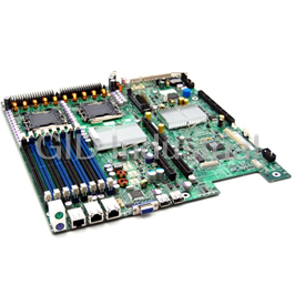
Intel 75-BB5000XAL CPU BOARD - 10pk MOTHERBD BB5000XAL 3

Intel 75-BLKD102GGC2L CPU Board - MOTHER BD BLKD102GGC2L MAT PCE16 PCI PE

Intel 75-BLKD915GAGL CPU Board - Desktop Board D915GAGL - Mainboard - micro ATX - i915G - LGA775
Intel 75-BLKD915GAGLKX CPU Board - 10 Pack, mATX, Intel 915G Express Chipset, Dual-channel DDR-400
Request a Quote

The quote request has been received
Close

Facing challenges or have inquiries? Feel free to contact us!
Call Us +1-469-283-2440
What they say about us
FANTASTIC RESOURCE
One of our top priorities is maintaining our business with precision, and we are constantly looking for affiliates that can help us achieve our goal. With the aid of GID Industrial, our obsolete product management has never been more efficient. They have been a great resource to our company, and have quickly become a go-to supplier on our list!
Bucher Emhart Glass
EXCELLENT SERVICE
With our strict fundamentals and high expectations, we were surprised when we came across GID Industrial and their competitive pricing. When we approached them with our issue, they were incredibly confident in being able to provide us with a seamless solution at the best price for us. GID Industrial quickly understood our needs and provided us with excellent service, as well as fully tested product to ensure what we received would be the right fit for our company.
Fuji
HARD TO FIND A BETTER PROVIDER
Our company provides services to aid in the manufacture of technological products, such as semiconductors and flat panel displays, and often searching for distributors of obsolete product we require can waste time and money. Finding GID Industrial proved to be a great asset to our company, with cost effective solutions and superior knowledge on all of their materials, it’d be hard to find a better provider of obsolete or hard to find products.
Applied Materials
CONSISTENTLY DELIVERS QUALITY SOLUTIONS
Over the years, the equipment used in our company becomes discontinued, but they’re still of great use to us and our customers. Once these products are no longer available through the manufacturer, finding a reliable, quick supplier is a necessity, and luckily for us, GID Industrial has provided the most trustworthy, quality solutions to our obsolete component needs.
Nidec Vamco
TERRIFIC RESOURCE
This company has been a terrific help to us (I work for Trican Well Service) in sourcing the Micron Ram Memory we needed for our Siemens computers. Great service! And great pricing! I know when the product is shipping and when it will arrive, all the way through the ordering process.
Trican Well Service
GO TO SOURCE
When I can't find an obsolete part, I first call GID and they'll come up with my parts every time. Great customer service and follow up as well. Scott emails me from time to time to touch base and see if we're having trouble finding something.....which is often with our 25 yr old equipment.
ConAgra Foods