Intel® Server Board
SE7520BB2
Technical Product Specification
Intel Order Number D43861-001
Revision 1.1
March, 2006
Enterprise Platforms and Services Division
Revision History Intel® Server Board SE7520BB2 Technical Product Specifictation
Revision History
Revision
Date Modifications
Number
11/2005 0.3 First draft
12/2005 0.5 Added memory subsystem detail and power budget
12/2005 0.7 Updated block diagram and server board power budget
02/2006 1.0 Updated diagrams, tables and notes
03/2006 1.1 Updated trademark information
Disclaimers
®
Information in this document is provided in connection with Intel products. No license, express or implied, by estoppel or otherwise,
to any intellectual property rights is granted by this document. Except as provided in Intel's Terms and Conditions of Sale for such
products, Intel assumes no liability whatsoever, and Intel disclaims any express or implied warranty, relating to sale and/or use of
Intel products including liability or warranties relating to fitness for a particular purpose, merchantability, or infringement of any
patent, copyright or other intellectual property right. Intel products are not intended for use in medical, life saving, or life sustaining
applications. Intel may make changes to specifications and product descriptions at any time, without notice.
Designers must not rely on the absence or characteristics of any features or instructions marked "reserved" or "undefined." Intel
reserves these for future definition and shall have no responsibility whatsoever for conflicts or incompatibilities arising from future
changes to them.
This document contains information on products in the design phase of development. Do not finalize a design with this information.
Revised information will be published when the product is available. Verify with your local sales office that you have the latest
datasheet before finalizing a design.
The Intel® Server Board SE7520BB2 may contain design defects or errors known as errata which may cause the product to deviate
from published specifications. Current characterized errata are available on request.
This document and the software described in it is furnished under license and may only be used or copied in accordance with the
terms of the license. The information in this manual is furnished for informational use only, is subject to change without notice, and
should not be construed as a commitment by Intel Corporation. Intel Corporation assumes no responsibility or liability for any errors
or inaccuracies that may appear in this document or any software that may be provided in association with this document.
Intel Corporation server baseboards contain a number of high-density VSLI and power delivery components, which need adequate
airflow to cool. Intel ensures through its own chassis development and testing that when Intel server building blocks are used
together, the fully integrated system will meet the intended thermal requirements of these components. It is the responsibility of the
system integrator that chooses not to use Intel developed server building blocks to consult vendor datasheets and operating
parameters to determine the amount of air flow required for their specific application and environmental conditions. Intel
Corporation cannot be held responsible, if components fail or the server board does not operate correctly when used outside any of
their published operating or non-operating limits.
Except as permitted by such license, no part of this document may be reproduced, stored in a retrieval system, or transmitted in any
form or by any means without the express written consent of Intel Corporation.
Intel, Pentium, Itanium, and Xeon are trademarks or registered trademarks of Intel Corporation.
*Other brands and names may be claimed as the property of others. Copyright © Intel Corporation 2006.
ii Revision 1.1
Intel® Server Board SE7520BB2 Technical Product Specification Table of Contents
Table of Contents
1. Introduction ..........................................................................................................................1
1.1 Purpose ...................................................................................................................1
1.2 Audience..................................................................................................................1
1.3 Document Outline ....................................................................................................1
1.4 Board Usage Disclaimer ..........................................................................................2
2. Product Overview.................................................................................................................3
2.1 Server Board Feature Set........................................................................................3
2.2 Server Board Illustration ..........................................................................................4
2.3 Mechanical Drawing ................................................................................................5
2.4 Server Board Layout................................................................................................6
2.5 Identifying the Version of an Intel® Server Board....................................................7
2.6 Chipset Overview.....................................................................................................7
2.6.1 Memory Controller Hub (MCH) ................................................................................7
2.6.2 Front Side Bus (FSB)...............................................................................................8
2.6.3 MCH Memory Sub-System Overview ......................................................................8
2.6.4 PCI Express.............................................................................................................8
2.6.5 Hub Interface ...........................................................................................................8
2.7 Processor Subsystem Detail....................................................................................9
2.7.2 Multiple Processor Initialization .............................................................................10
2.7.3 Processor VRD ......................................................................................................10
2.7.4 Reset Configuration Logic .....................................................................................11
2.7.5 Processor Module Presence Detection .................................................................11
2.7.6 GTL2006* ..............................................................................................................11
2.7.7 Common Enabling Kit (CEK) Design Support .......................................................12
2.8 Memory Sub-System Detail ...................................................................................13
2.8.1 Memory Sizing .......................................................................................................13
2.8.2 Disabling DIMMs....................................................................................................14
2.8.3 ECC Memory Initialization .....................................................................................15
2.8.4 Memory Population................................................................................................15
2.8.5 Memory Error Handling..........................................................................................16
2.8.6 Memory Test..........................................................................................................18
2.8.7 Memory RASUM Features.....................................................................................18
2.8.8 Logging Memory RAS Information to the SEL.......................................................25
2.8.9 High Memory Gap Reclaiming...............................................................................27
2.9 PCI Sub-System Detail ..........................................................................................27
2.9.1 ICH5-R PCI Interface.............................................................................................27
2.9.2 PXH .......................................................................................................................31
2.10 IO Sub-System Detail ............................................................................................35
Revision 1.1 iii
Table of Contents Intel® Server Board SE7520BB2 Technical Product Specification
2.10.1 Server I/O ..............................................................................................................35
2.10.2 Intel® 3-Volt Advanced+ Boot Block Flash Memory..............................................35
2.10.3 Video Controller .....................................................................................................36
2.11 Clock Generation and Distribution .........................................................................36
2.11.1 CK409 Clock Generator.........................................................................................36
2.11.2 DB800 Differential Buffer .......................................................................................37
3. BIOS Architecture ..............................................................................................................38
3.1 BIOS Functionality .................................................................................................38
3.1.1 Support for BIOS Features ....................................................................................38
3.1.2 BIOS Identification String.......................................................................................42
3.1.3 Hardware Requiring BIOS Support........................................................................43
3.1.4 BIOS POST ...........................................................................................................43
3.1.5 User Interface ........................................................................................................43
3.2 BIOS Setup Utility ..................................................................................................44
3.2.1 Entering BIOS Setup .............................................................................................44
3.3 Keyboard Commands ............................................................................................44
3.4 Entering BIOS Setup .............................................................................................46
3.4.1 Main Menu .............................................................................................................46
3.4.2 Advanced Menu.....................................................................................................46
3.4.3 Boot Menu .............................................................................................................57
3.4.4 Security Menu........................................................................................................59
3.4.5 Server Menu ..........................................................................................................61
3.4.6 Exit Menu...............................................................................................................64
3.5 Other BIOS Configuration Utilities .........................................................................65
3.5.1 Flash Update Utility................................................................................................65
3.6 Localization Details................................................................................................66
3.7 Flash Architecture and Flash Update Utility...........................................................66
3.7.1 Rolling BIOS and On-line Updates ........................................................................66
3.7.2 Flash Update Utility................................................................................................67
3.7.3 User Binary Area ...................................................................................................68
3.7.4 Recovery Mode......................................................................................................69
3.7.5 Update OEM Logo .................................................................................................71
3.8 OEM Binary ...........................................................................................................72
3.9 PCI Numeration .....................................................................................................74
3.10 ACPI Runtime Checkpoints ...................................................................................75
4. Platform Management Architecture..................................................................................76
4.1 Management Architecture Overview......................................................................76
4.1.1 Tiered Server Management Model ........................................................................76
4.1.2 5V Standby ............................................................................................................79
4.1.3 IPMI Messaging, Commands, and Abstractions....................................................80
4.1.4 IPMI ‘Sensor Model’...............................................................................................80
iv Revision 1.1
Intel® Server Board SE7520BB2 Technical Product Specification Table of Contents
4.1.5 Private Management Buses...................................................................................81
4.1.6 Management Controllers .......................................................................................81
4.2 Essentials Management Features and Functionality .............................................93
4.2.1 Overview of mBMC................................................................................................93
4.2.2 mBMC Self-test......................................................................................................94
4.2.3 SMBus Interfaces ..................................................................................................94
4.2.4 External Interface to mBMC...................................................................................94
4.2.5 Messaging Interfaces.............................................................................................95
4.2.6 Direct Platform Control (IPMI over LAN)................................................................97
4.2.7 Wake On LAN / Power On LAN and Magic Packet Support................................100
4.2.8 Watchdog Timer ..................................................................................................100
4.2.9 System Event Log (SEL) .....................................................................................100
4.2.10 Sensor Data Record (SDR) Repository ...............................................................101
4.2.11 Event Message Reception...................................................................................101
4.2.12 Event Filtering and Alerting..................................................................................101
4.2.13 NMI Generation ...................................................................................................104
4.2.14 SMI Generation....................................................................................................104
4.3 Platform Management Interconnects...................................................................105
4.3.1 Power Supply Interface Signals...........................................................................105
4.3.2 System Reset Control..........................................................................................106
4.3.3 Fan Speed Control...............................................................................................107
4.3.4 Front Panel Control..............................................................................................107
4.3.5 FRU Information ..................................................................................................111
4.4 Sensors................................................................................................................111
4.4.1 Sensor Type Codes .............................................................................................111
4.5 Server Management Block Diagram....................................................................115
4.5.1 Management Buses and Connectors ..................................................................116
4.5.2 SIO Keyboard and Mouse ...................................................................................116
4.5.3 PS2 Keyboard and Mouse...................................................................................116
4.5.4 Fast Management Link (FML)..............................................................................116
4.5.5 LPC/Keyboard Controller Style Ports ..................................................................117
4.5.6 USB .....................................................................................................................118
2
4.5.7 I C Interfaces .......................................................................................................118
4.5.8 16550* UARTs.....................................................................................................119
4.5.9 Interrupts..............................................................................................................119
4.5.10 GPIO Pins and LED Drivers ................................................................................119
4.5.11 Sleep States Supported.......................................................................................119
4.5.12 Wake Events........................................................................................................120
4.5.13 AC Power Failure Recovery ................................................................................120
4.5.14 PCI Power Management Support ........................................................................121
4.6 System Status Indicators/LEDs ...........................................................................121
Revision 1.1 v
Table of Contents Intel® Server Board SE7520BB2 Technical Product Specification
4.6.1 Front Panel ..........................................................................................................122
5. Error Reporting and Handling.........................................................................................125
5.1 Error Propagation ................................................................................................125
5.2 Fault Resilient Booting (FRB) ..............................................................................125
5.2.1 FRB-3 – BSP Reset Failures ...............................................................................125
5.2.2 FRB-2 – BSP POST Failures...............................................................................125
5.2.3 FRB-1 – BSP Self-Test Failures ..........................................................................126
5.2.4 OS Boot Timer - OS Load Failures......................................................................126
5.2.5 Application Processor (AP) Failures ....................................................................126
5.2.6 Treatment of Failed Processors...........................................................................126
5.3 Error Messages and Error Codes ........................................................................127
5.3.1 POST Error Codes and Messages ......................................................................127
5.3.2 POST Error Beep Codes .....................................................................................130
5.3.3 Checkpoints.........................................................................................................130
5.4 Error Logging .......................................................................................................132
5.4.1 Error Sources and Types.....................................................................................132
5.4.2 SMI Handler.........................................................................................................133
5.4.3 Logging Format Conventions...............................................................................134
5.4.4 POST Code Checkpoints.....................................................................................139
5.4.5 Boot Block Initialization Code Checkpoints .........................................................141
5.4.6 Boot Block Recovery Code Checkpoint...............................................................142
5.4.7 DIM Code Checkpoints........................................................................................143
5.4.8 Single-bit ECC Error Throttling Prevention ..........................................................143
5.5 Reliability, Availability and Serviceability (RAS) Features ...................................144
5.5.1 Memory RAS features .........................................................................................144
5.5.2 PCI Express.........................................................................................................144
5.5.3 RAS Features of FSB ..........................................................................................145
5.5.4 PCI-X ...................................................................................................................145
5.5.5 RMC Connector Utilization ..................................................................................145
5.5.6 Rolling BIOS ........................................................................................................146
6. Connector Pin-outs and Jumper Blocks........................................................................147
6.1 Board Connector Pin-outs ...................................................................................147
6.2 Board Jumper Blocks...........................................................................................153
6.2.1 Rolling BIOS Bank Selection Jumper ..................................................................153
6.2.2 BIOS Recovery ....................................................................................................153
6.2.3 Password Clear ...................................................................................................153
6.2.4 CMOS Clear ........................................................................................................153
7. Environmental Specifications .........................................................................................155
7.1 Environmental Specifications and Cooling Requirements ...................................155
7.2 Power Supply Requirements ...............................................................................156
7.2.1 Baseboard Power Budget....................................................................................156
vi Revision 1.1
Intel® Server Board SE7520BB2 Technical Product Specification Table of Contents
7.2.2 Voltages Supported .............................................................................................157
7.2.3 Standby Powered Device Map ............................................................................158
7.2.4 System Reset Block Diagram ..............................................................................158
7.3 Airflow Requirements...........................................................................................161
7.3.1 Board Usage Disclaimer ......................................................................................161
7.4 Board Level Calculated MTBF Data ....................................................................161
7.4.1 Intel SpeedStep® Technology.............................................................................161
7.5 Product Regulatory Compliance ..........................................................................161
7.5.1 Product Safety Compliance .................................................................................161
7.5.2 Product EMC Compliance ...................................................................................162
7.5.3 Mandatory/Standard: Certifications, Registration, Declarations ..........................162
7.5.4 Product Regulatory Compliance Markings ..........................................................162
7.5.5 Electromagnetic Compatibility Notices ................................................................163
7.5.6 Replacing the Back up Battery ............................................................................163
Glossary...................................................................................................................................165
Reference Documents ............................................................................................................166
Revision 1.1 vii
List of Figures Intel® Server Board SE7520BB2 Technical Product Specification
List of Figures
Figure 1. Top Side View of the Intel® Server Board SE7520BB2 ...............................................4
®
Figure 2. Intel Server Board SE7520BB2 Server Board Mechanical Drawing ...........................5
Figure 3. Intel® Server Board SE7520BB2 Block Diagram .........................................................6
Figure 4. CEK Processor Mounting ............................................................................................12
Figure 5. Identifying Banks of Memory .......................................................................................14
Figure 6. Four DIMM Memory Mirror Configuration ....................................................................22
Figure 7. Six DIMM Memory Mirror Configuration ......................................................................23
Figure 8. Eight DIMM Memory Mirror Configuration ...................................................................24
Figure 9. Block Diagram of Platform Managment Architecture..................................................79
Figure 10. mBMC in a Server Management System .................................................................93
Figure 11. External Interfaces to mBMC....................................................................................95
Figure 12. IPMI-over-LAN ..........................................................................................................98
Figure 13. Power Supply Control Signals ................................................................................105
Figure 14. Server Management Block Diagram........................................................................115
Figure 15. Front Panel Pinout ..................................................................................................123
Figure 16. SE7520BB2 Jumper Block Locations ......................................................................154
Figure 17. Reset and PowerGood Timings..............................................................................159
Figure 18. Intel® Server Board SE7520BB2 Power Sequencing Diagram..............................160
viii Revision 1.1
Intel® Server Board SE7520BB2 Technical Product Specification List of Tables
List of Tables
Table 1. Processor Support Matrix ..............................................................................................9
Table 2. DIMM Module Capacities..............................................................................................13
Table 3. Supported DDR2-400 DIMM Populations .....................................................................16
Table 4. Memory Error Handling in RAS Mode...........................................................................17
Table 5. Memory Error Handling in Non-RAS Mode...................................................................17
Table 6. Memory RAS Events.....................................................................................................26
Table 7. GPIO on the Intel® Server Board SE7520BB2............................................................30
Table 8. Slot 6 PCI-X Pin-out.....................................................................................................32
Table 9. BIOS Setup Keyboard Command Bar Options .............................................................44
Table 10. BIOS Setup, Main Menu Options................................................................................46
Table 11. BIOS Setup, Advanced Menu Options........................................................................46
Table 12. BIOS Setup, Processor Configuration Sub-menu Options .........................................47
Table 13. BIOS Setup IDE Configuration Menu Options ............................................................48
Table 14. Mixed P-ATA-S-ATA Configuration with only Primary P-ATA.....................................49
Table 15. BIOS Setup, IDE Device Configuration Sub-menu Selections ...................................50
Table 16. BIOS Setup, Floppy Configuration Sub-menu Selections...........................................51
Table 17. BIOS Setup, Super I/O Configuration Sub-menu........................................................51
Table 18. BIOS Setup, USB Configuration Sub-menu Selections ..............................................52
Table 19. BIOS Setup, USB Mass Storage Device Configuration Sub-menu Selections...........53
Table 20. BIOS Setup, PCI Configuration Sub-menu Selections ...............................................53
Table 21. BIOS Setup, Memory Configuration Sub-menu Selections ........................................54
Table 22. BIOS Setup, Boot Menu Selections............................................................................57
Table 23. BIOS Setup, Boot Settings Configuration Sub-menu Selections ................................57
Table 24. BIOS Setup, Boot Device Priority Sub-menu Selections ............................................58
Table 25. BIOS Setup, Hard Disk Drive Sub-Menu Selections...................................................58
Table 26. BIOS Setup, Removable Drives Sub-menu Selections ..............................................58
Table 27. BIOS Setup, CD/DVD Drives Sub-menu Selections...................................................59
Table 28. BIOS Setup, Security Menu Options...........................................................................59
Table 29. BIOS Setup, Server Menu Selections.........................................................................61
Table 30. BIOS Setup, System Management Sub-menu Selections..........................................62
Table 31. BIOS Setup, Serial Console Features Sub-menu Selections .....................................63
Table 32. BIOS Setup, Event Log Configuration Sub-menu Selections .....................................64
Table 33. BIOS Setup, Exit Menu Selections .............................................................................64
Table 34. ACPI Runtime Checkpoints .......................................................................................75
Table 35. Tiered Platform Management Feature Overview .......................................................76
Table 36. Power and Reset Control...........................................................................................77
Table 37. Secure Mode Button Actions .....................................................................................78
Table 38. Memory RAS Feature Support by Server Management Tier .....................................78
Revision 1.1 ix
List of Tables Intel® Server Board SE7520BB2 Technical Product Specification
Table 39. mBMC Built-in Sensors..............................................................................................84
Table 40. Onboard Platform Instrumentaion using the mBMC ..................................................85
Table 41. Platform Instrumentation Sensors using the Intel® Management Module.................87
Table 42. Supported Channel Assigments ................................................................................96
Table 43. LAN Channel Capacity...............................................................................................97
Table 44. LAN Channel Specifications ......................................................................................99
Table 45. PEF Action Priorities................................................................................................102
Table 46. mBMC Factory Default Event Filters........................................................................102
Table 47. Power Control Initiators............................................................................................106
Table 48. System Reset Sources and Actions.........................................................................107
Table 49. Chassis ID LEDs......................................................................................................109
Table 50. Fault/Status LED......................................................................................................109
Table 51. mBMC Built-in Sensors............................................................................................112
Table 52. Intel® Server Board SE7520BB2 Platform Sensors for Essentials Management....113
Table 53. Front Panel Color Attributes.....................................................................................123
Table 54. Error Codes and Messages .....................................................................................127
Table 55. Error Codes Sent to Management Module ..............................................................129
Table 56. POST Error Beep Codes .........................................................................................130
Table 57. Troubleshooting BIOS Beep Codes.........................................................................130
Table 58. POST Progress Code LED Example .......................................................................131
Table 59. Memory Error Codes................................................................................................131
Table 60. Memory Error Events ...............................................................................................135
Table 61. Examples of Event Data Field Contents for Memory Errors ....................................135
Table 62. PCI Error Events ......................................................................................................137
Table 63. Examples of Event Data Field Contents for PCI Errors ...........................................137
Table 64. FRB-2 Error Events..................................................................................................138
Table 65. Examples of Event Data Field Contents for FRB-2 Errors.......................................138
Table 66. POST Code Checkpoints.........................................................................................139
Table 67. Boot block Initialization Code Checkpoints ..............................................................141
Table 68. Boot Block Recovery Code Checkpoint ...................................................................142
Table 69. Boot Block Recovery Beep Code.............................................................................142
Table 70. DIM Code Checkpoints ............................................................................................143
Table 71. Board Connector Matrix ...........................................................................................147
Table 72. Test Support Connector...........................................................................................147
Table 73. OEM RMC 8-pin (Remote Management Card Support) ..........................................148
Table 74. EPS12V 2x12 Connector .........................................................................................148
Table 75. EPS12V 2x4 Connector ...........................................................................................149
Table 76. EPS12V 1x5 Connector ...........................................................................................149
Table 77. Primary IDE Connector ............................................................................................149
Table 78. Front Panel Connector.............................................................................................150
Table 79. USB Front Connector...............................................................................................150
x Revision 1.1
Intel® Server Board SE7520BB2 Technical Product Specification List of Tables
Table 80. USB Rear Connector ...............................................................................................150
Table 81. SATA Connector......................................................................................................151
Table 82. Battery Holder ..........................................................................................................151
Table 83. Piezo* Speaker ........................................................................................................151
Table 84. Fan 1 and Fan 2 (3 Pin + 2 Pin)...............................................................................151
Table 85. Fan 3 and Fan 4.......................................................................................................151
Table 86. Fan 5 and Fan 6.......................................................................................................152
Table 87. BIOS Bank Selection Jumper ..................................................................................153
Table 88. BIOS Recovery Jumper Setting ...............................................................................153
Table 89. Password Clear Jumper Setting ..............................................................................153
Table 90. CMOS Clear Jumper Setting ...................................................................................153
Table 91. Baseboard Power Budget ........................................................................................156
Table 92. Intel® Server Board SE7520BB2 Board Voltage Table...........................................157
Revision 1.1 xi
List of Tables Intel® Server Board SE7520BB2 Technical Product Specification
xii Revision 1.1
Intel® Server Board SE7520BB2 Technical Product Specification Introduction
1. Introduction
1.1 Purpose
®
This Intel Server Board SE7520BB2 Technical Product Specification (TPS) provides technical
details on the functional architecture and feature set of the server board.
1.2 Audience
This document is intended for technical personnel requiring a technical overview of the Server
Board SE7520BB2. Familiarity with Intel® server architecture, Intel® processor architecture,
memory technologies and the Peripheral Component Interconnect (PCI) local bus architecture is
assumed.
1.3 Document Outline
This document is composed of the following chapters:
Chapter 1: Introduction
Chapter 2: Product Overview
Chapter 3: Board Architecture
Chapter 4: BIOS
Chapter 5: Platform Management Architecture
Chapter 6: Error Reporting and Handling
Chapter 7: Connector Pin-outs and Jumper Blocks
Chapter 8: Environmental Specifications
Chapter 9: Other Useful Information
Revision 1.1 Intel Confidential 1
Introduction Intel® Server Board SE7520BB2 Technical Product Specification
1.4 Board Usage Disclaimer
Intel Corporation server baseboards contain a number of high-density VLSI and power delivery
components that need adequate airflow to cool. It is the responsibility of the system integrator to
consult vendor datasheets and operating parameters to determine the amount of airflow
required for their specific application and environmental conditions. Intel Corporation cannot be
held responsible if components fail or the server board does not operate correctly when used
outside any of its published operating or non-operating limits.
2 Revision 1.1
Intel® Server Board SE7520BB2 Technical Product Specification Product Overview
2. Product Overview
The Server Board SE7520BB2 is an Intel® Architecture (IA) 32-based server board capable of
supporting two Dual-Core Intel® Xeon™ processor LV, and is optimized for high performance
computing environments leveraging extremely low power consumption per compute node. The
platform is based on the Intel® E7520 chipset and incorporates several new high-speed buses
and signaling architectures.
2.1 Server Board Feature Set
The Server Board SE7520BB2 supports the following feature set:
• IA-32 server platform based on the Intel® E7520 chipset
• Two Dual-Core Intel® Xeon™ processors LV with 667MHz FSB
• Eight DDR2 DIMM sockets supporting DDR2-400 Registered ECC memory (two
memory channels with four DIMMs per channel, four bank)
• Intel® 82801ER I/O Controller Hub (ICH5-R), interfaced with an Intel® E7520 Memory
Controller Hub (MCH) via Hub Interface 1.5
• PXH PCI-X bridge, interfaced with the MCH via x8 PCI Express Interface supporting
one PCI-X 2.0 133-MHz slot
• One PCI Express x8 slot via direct PCI Express x8 interface to MCH
• Marvell* ““Yukon”” 88E8050 10/100/1000 LAN, interfaces with the MCH via x1 PCI
Express Interface
• Intel® 82541PI supporting 10/100/1000 LAN, interface with the ICH5-R via PCI 32/33
bus
• LPC server I/O
• Onboard PCI ATI* Rage XL video controller
• Two USB 2.0 (USB 1-2) ports in rear IO panel
• Two USB 2.0 (USB 3-4) via header on the board
• Dual SATA Interfaces
• 2 SATA 1.0 ports via ICH5-RR controller (SATA_A0, SATA_A1)
• 4 SATA 2.0 ports via Silicon Image controller (SATA_B0, SATA_B1, SATA_B2,
SATA_B3)
• Single ATA-100 interface
• One serial port on rear IO panel
• Second serial port via header on the board
• One floppy connector
Revision 1.1 Intel Confidential 3
Product Overview Intel® Server Board SE7520BB2 Technical Product Specification
2.2 Server Board Illustration
The following figure provides a high-level illustration of the Server Board SE7520BB2.
Figure 1. Top Side View of the Intel® Server Board SE7520BB2
4 Revision 1.1
Intel® Server Board SE7520BB2 Technical Product Specification Product Overview
2.3 Mechanical Drawing
The following figure provides a mechanical illustration of the Server Board SE7520BB2.
®
Figure 2. Intel Server Board SE7520BB2 Server Board Mechanical Drawing
Revision 1.1 Intel Confidential 5
Product Overview Intel® Server Board SE7520BB2 Technical Product Specification
2.4 Server Board Layout
Figure 3. below illustrates the functional blocks of the Server Board SE7520BB2 as well as the
plug-in modules that the server board supports.
Figure 3. Intel® Server Board SE7520BB2 Block Diagram
6 Revision 1.1
Intel® Server Board SE7520BB2 Technical Product Specification Product Overview
2.5 Identifying the Version of an Intel® Server Board
The version of an Intel® server board can be determined from the last three digits of the board
part number.
Example part number: C44686-703
7 = Fabrication (FAB) number
03 = Revision 3
The board part number can be found on the server board silkscreen. It can also be determined
by using Intel® Server Management or by checking the System Management sub-menu in BIOS
Setup. See Table 30. BIOS Setup, System Management Sub-menu Selections
2.6 Chipset Overview
®
The architecture of the Server Board SE7520BB2 is designed around the Intel E7520 chipset.
The chipset consists of three components, which together are responsible for providing the
interface between all major sub-systems found on the baseboard, including the processor,
memory, and I/O sub-systems. These three components are:
• Memory Controller Hub (MCH)
• I/O Controller Hub (ICH5-R)
• Intel® 6700PXH 64-bit Hub (PXH)
The MCH is configured to support the following interfaces:
• CPU Front Side Bus at 667MHz operation using AGTL+ (Assisted Gunning Transceiver
Logic) signaling, 4x 64 bit data bus at 6.4 GB/s.
• Dual memory channels supporting registered 72-bit data ECC DIMMs for DDR2-400.
DDR bandwidth of 2.13/2.6 GB/s per channel giving 4.26 GB/s for both.
• Three PCI Express x8 interfaces with aggregate bandwidth of 4 GB/s interfaces to PXH
and other onboard devices. Each of these interfaces can be configured as two
independent x4 interfaces.
• Hub Interface 1.5, 8 bits, 66 MHz, 266MB/s interface to the ICH5-R.
• Debug support through XDP (Extended Debug Port) connector.
• RASUM support through memory features and SMBus debug port access.
2.6.1 Memory Controller Hub (MCH)
The MCH uses a 1077-ball FC-BGA package in which it integrates four main functions:
• Front Side Bus
• Memory controller
• PCI-Express controller
• Hub Link controller
Revision 1.1 Intel Confidential 7
Product Overview Intel® Server Board SE7520BB2 Technical Product Specification
2.6.2 Front Side Bus (FSB)
The Intel® E7520 MCH supports either single or dual population of the Dual-Core Intel® Xeon™
processor LV. The MCH supports a base system bus frequency of 166MHz. The address and
request interface is double pumped at 333MHz while the 64-bit data interface (+ parity) is quad
pumped to 667MHz. This provides a matched system bus address and data bandwidths of
6.4GB/sec.
2.6.3 MCH Memory Sub-System Overview
The MCH provides an integrated memory controller for direct connection to two channels of
registered DDR2-400 memory (ECC or non-ECC). Peak theoretical memory data bandwidth
using DDR2-400 technology is 6.4GB.
When both DDR2 channels are populated and operating, they function in lock-step mode. For
the Intel® E7520 MCH, the maximum supported DDR2-400 memory size is 16GB.
There are several Reliability, Availability, Serviceability, Usability and Manageability (RASUM)
features for the MCH memory interface:
• Memory mirroring allows for two copies of all data in the memory subsystem (one on
each channel) to be maintained
• DIMM sparing allows for one DIMM per channel to be held in reserve and brought on-
line if another DIMM in the channel becomes defective. DIMM sparing and memory
mirroring are mutually exclusive of one another.
• Hardware periodic memory scrubbing, including demand scrub support
• Retry on uncorrectable memory errors
• Intel® Single Device Data Correction (SDDC) x4 for memory error detection and
correction of any number of single bit failures in a single x4 memory device
Note: DIMM sparing and memory mirroring are mutually exclusive.
2.6.4 PCI Express
The Intel® E7520 MCH is the first Intel® chipset to support the new PCI Express* high-speed
serial I/O interface for superior I/O bandwidth. The scalable PCI Express interface complies with
the PCI Express* Interface Specification, Rev 1.0a. The MCH provide three x8 PCI Express
interfaces, each with a maximum theoretical bandwidth of 4 GB/s.
The Intel® E7520 MCH is a root class component as defined in the PCI Express Interface
Specification, Rev 1.0a. The PCI Express interfaces of the MCH support connection to a variety
of bridges and devices compliant with the same revision of the PCI Express Interface
Specification, Rev 1.0a. Refer to the Intel® Server Board SE7520BB2 Tested Hardware and OS
List for add-in cards tested on this platform.
2.6.5 Hub Interface
The MCH interfaces with the Intel® 82801ER I/O Controller Hub 5-R (ICH5-R) via a dedicated
Hub Interface supporting a peak bandwidth of 266MB/s using a x4 base clock of 66 MHz.
8 Revision 1.1
Intel® Server Board SE7520BB2 Technical Product Specification Product Overview
2.7 Processor Subsystem Detail
The Server Board SE7520BB2 is designed to support one or two Dual-Core Intel® Xeon™
processors LV with frequencies starting at 1.67GHz, 2.0GHz and beyond. These processors
use Intel’s 65-nanometer technology and an 667MHz front side bus. When two processors are
installed, both must be of identical revision, core voltage, cache size, and bus/core speed.
When only one processor is installed, it should be in the socket labeled “CPU1”, and the other
socket must be empty. The support circuitry on the server board consists of the following:
Note: Previous generations of the Intel® Xeon™ processor are not supported on the Intel®
Server Board SE7520BB2.
• Dual 479pin zero insertion force (ZIF) processor sockets
• Processor host bus AGTL+ support circuitry
• Reset configuration logic
• Processor module presence detection logic
• BSEL detection capabilities
• CPU signal level translation
• CEK CPU retention support.
Table 1. Processor Support Matrix
Processor Package Type FSB Technology Frequency Cache Support
Family Frequency Size
Dual-Core
FC-mPGA4 667 MHz 65 nM 2.0 GHz 2048KB Yes
Intel® Xeon™
Processor LV
Dual-Core
FC-mPGA4 667 MHz 65 nM 1.67 GHz 2048KB Yes
Intel® Xeon™
Processor LV
The Server Board SE7520BB2 is designed to provide up to 12A per processor. Processors with
higher current requirements are not supported.
2.7.1.1 Mixed Processor Steppings
For optimum system performance, only identical processors should be installed in a system.
Processor steppings can be mixed in a system provided that there is no more than a 1-stepping
difference in all processors installed. If the installed processors are more than 1-stepping apart,
an error (8080 through 8183) is logged in the System Event Log (SEL) and an error (01298000
through 01298003) is reported to the Management Module. Acceptable mixed steppings are not
reported as errors.
2.7.1.2 Mixed Processor Models
Processor models cannot be mixed in a system. If this condition is detected, an error (8196) is
logged in the SEL.
2.7.1.3 Mixed Processor Families
Processor families cannot be mixed in a system. If this condition is detected, an error (8194) is
logged in the SEL.
Revision 1.1 Intel Confidential 9
Product Overview Intel® Server Board SE7520BB2 Technical Product Specification
2.7.1.4 Mixed Processor Cache Sizes
If the installed processors have mixed cache sizes, an error (8192) will be logged in the SEL
and an error (196) is reported to the Management Module. The size of all cache levels must
match between all installed processors. Mixed cache processors are not supported.
2.7.1.5 Microcode
IA-32 processors have the capability of correcting specific errata through the loading of an Intel-
supplied data block (microcode update). The BIOS is responsible for storing the update in
nonvolatile memory and loading it into each processor during POST. The BIOS performs all the
recommended update signature verification prior to storing the update in the Flash.
2.7.1.6 Processor Cache
The BIOS enables all levels of processor cache as early as possible during POST. There are no
user options to modify the cache configuration, size or policies. All detected cache sizes are
reported in the SMBIOS Type 7 structures. The largest and highest level cache detected is
reported in BIOS Setup.
2.7.2 Multiple Processor Initialization
IA32 processors have a microcode-based BSP-arbitration protocol. On reset, all of the
processors compete to become the bootstrap processor (BSP). If a serious error is detected
during a Built-in Self-Test (BIST), that processor will not participate in the initialization protocol.
A single processor that successfully passes BIST is automatically selected by the hardware as
the BSP and starts executing from the reset vector (F000:FFF0h). A processor that does not
perform the role of BSP is referred to as an application processor (AP).
The BSP is responsible for executing the BIOS power-on self-test (POST) and preparing the
machine to boot the operating system. At boot time, the system is in virtual wire mode and the
BSP alone is programmed to accept local interrupts (INTR driven by programmable interrupt
controller (PIC) and non-maskable interrupt (NMI)). For single processor configurations, the
system is put in the virtual wire mode, which uses the local APIC of the processor.
As a part of the boot process, the BSP wakes each AP. When awakened, an AP programs its
Memory Type Range Registers (MTRRs) to be identical to those of the BSP. All APs execute a
halt instruction with their local interrupts disabled. The System Management Mode (SMM)
handler expects all processors to respond to an SMI. If the BSP determines that an AP exists
that is a lower-featured processor or that has a lower value returned by the CPUID function, the
BSP will switch to the lowest-featured processor in the system.
2.7.3 Processor VRD
The Server Board SE7520BB2 has two VRDs (Voltage Regulator Down) providing the
appropriate voltages to the installed processors. Each VRD is compliant with the EmVRD 11.0
specification and is designed to support current and next generation Dual-Core Intel® Xeon™
processors LV that require up to a sustained maximum of 36A and peak support of 45A.
The baseboard supports Flexible Mother Board (FMB) for all Dual-Core Intel® Xeon™
processors LV with respect to current requirements and processor speed requirements. FMB is
an estimation of the maximum values the processors will have over their lifetime. The value is
only an estimate and actual specifications for future processors may differ. Currently, the
demand per FMB is a sustained maximum of 36 Amps and a peak support of 45 Amps.
10 Revision 1.1
Intel® Server Board SE7520BB2 Technical Product Specification Product Overview
2.7.4 Reset Configuration Logic
The BIOS determines the processor stepping, cache size, etc., through the CPUID instruction.
All processors in the system must operate at the same frequency, have the same cache size,
and have the same voltage identification (VID). No mixing of product families is supported.
Processors run at a fixed speed and cannot be programmed to operate at a lower or higher
speed.
2.7.5 Processor Module Presence Detection
Logic is provided on the baseboard to detect the presence and identity of installed processors.
In dual-processor configurations, the onboard mini Baseboard Management Controller (mBMC)
must read the processor VID bits for each processor before turning on the VRD. If the VIDs of
the two processors are not identical, then the BMC will not turn on the VRD.
The following circuit is designed to ensure that three criteria are met prior to enabling the
embedded VRD:
• Ensure that in a UP configuration, the end agent CPU (P1) is installed
• Disable older-generation Dual-Core Intel® Xeon™ processors LV from running in the
system to prevent damage to the MCH
• Ensure in a DP configuration that both processors support the same FSB frequency
2.7.6 GTL2006*
The GTL2006* is a 13-bit translator designed for 3.3V to GTL/GTL+ translations to the system
bus. The translator incorporates all the level shifting and logic functions required to interface
between the processor subsystem and the rest of the system.
Revision 1.1 Intel Confidential 11
Product Overview Intel® Server Board SE7520BB2 Technical Product Specification
2.7.7 Common Enabling Kit (CEK) Design Support
The server board has been designed to comply with Intel’s Common Enabling Kit (CEK)
processor mounting and heatsink retention solution. The server board as shipped from Intel’s
factory will ship with a CEK spring snapped onto the bottom side of the board beneath each
processor socket. The CEK spring is removable allowing for the use of non-Intel heatsink
retention solutions and single processor configurations.
Heatsink assembly
Thermal Interface
Material (TIM)
TP02091
Server Board
CEK Spring
Chassis
AF000196
Figure 4. CEK Processor Mounting
Note: Due to the forces exerted on the processor socket when a CPU is not present, users must
remove the CEK spring associated with the empty socket from the server board for single
processor configurations. This ensures proper structural integrity of the empty socket location
for future use.
12 Revision 1.1
Intel® Server Board SE7520BB2 Technical Product Specification Product Overview
2.8 Memory Sub-System Detail
2.8.1 Memory Sizing
The E7520 MCH provides an integrated memory controller for direct connection to two channels
of registered DDR2-400 memory (stacked or unstacked). Peak theoretical memory data
bandwidth using DDR2-400 technology is 6.4 GB/s.
The memory controller is capable of supporting up to 4 loads per channel for DDR2-400.
Memory technologies are classified as being either single rank or dual rank depending on the
number of DRAM devices that are used on any one DIMM. A single rank DIMM is a single load
device, ie) Single Rank = 1 Load. Dual rank DIMMs are dual load devices, ie) Dual Rank = 2
loads.
The Server Board SE7520BB2 provides the following maximum memory capacities based on
the number of DIMM slots provided and maximum supported memory loads by the chipset:
• 16GB maximum capacity for DDR2-400
The minimum memory supported with the system running in single-channel memory mode is:
• 256MB for DDR2-400.
Supported DIMM capacities are as follows:
• DDR2-400 Memory DIMM sizes include: 256MB, 512MB, 1GB, 2GB, and 4GB.
Table 2. DIMM Module Capacities
SDRAM Parts / SDRAM Technology Used 256Mb 512Mb 1Gb
X8, single row 256MB 512MB 1GB
X8, double row 512MB 1GB 2GB
X4, single row 512MB 1GB 2GB
X4, Stacked, double row 1GB 2GB 4GB
DIMMs on channel ‘A’ are paired with DIMMs on channel ‘B’ to configure 2-way interleaving.
Each DIMM pair is referred to as a bank. The bank can be further divided into two rows, based
on single-sided or double-sided DIMMs. If both DIMMs in a bank are single-sided, only one row
is said to be present. For double-sided DIMMs, both rows are said to be present.
The Server Board SE7520BB2 has eight DIMM slots (four DIMM banks). Both DIMMs in a bank
should be identical (same manufacturer, CAS latency, number of rows, columns and devices,
timing parameters etc.). Although DIMMs within a bank must be identical, the BIOS supports
various DIMM sizes and configurations allowing the banks of memory to be different. Memory
sizing and configuration is guaranteed only for qualified DIMMs approved by Intel.
Revision 1.1 Intel Confidential 13
DIMM 1B
DIMM 1A
DIMM 2B
DIMM 2A
DIMM 3B
DIMM 3A
DIMM 4B
DIMM 4A
Product Overview Intel® Server Board SE7520BB2 Technical Product Specification
MCH
Bank 4 Bank 3 Bank 2 Bank 1
Figure 5. Identifying Banks of Memory
The BIOS reads the Serial Presence Detect (SPD) SEEPROMs on each installed memory
module to determine the size and timing of the installed memory modules. The memory-sizing
algorithm determines the size of each bank of DIMMs. The BIOS programs the memory
controller in the chipset accordingly. The total amount of configured memory can be found using
BIOS Setup.
2.8.2 Disabling DIMMs
The BIOS provides a mechanism to disable a DIMM if it is detected to be faulty. A faulty DIMM
is defined as a DIMM that either has multiple correctable errors or a single uncorrectable error.
Faulty DIMM(s) are taken off-line during the POST memory test. During runtime, memory errors
are logged and single-bit ECC errors are counted. Disabling DIMM(s) during runtime is only
®
supported if an Intel Management Module is installed. Although DIMMs are marked as
“disabled”, they are actually disabled only during the next reboot.
On system boot, memory-sizing code reads the recorded state of the DIMMs and skips sizing
DIMM(s) which were previously marked as disabled. If all DIMMs in a system have been
disabled, the BIOS will re-enable all DIMMs.
Disabled DIMMs/rows may be re-enabled through a BIOS Setup option. The DIMM slot will no
longer be disabled if the system boots without memory in the DIMM slot.
14 Revision 1.1
Intel® Server Board SE7520BB2 Technical Product Specification Product Overview
2.8.3 ECC Memory Initialization
ECC memory must be initialized by the BIOS before it can be used. The BIOS must initialize all
memory locations before using them. The BIOS uses the auto-initialize feature of the MCH to
initialize ECC. ECC memory initialization cannot be aborted and may result in a noticeable delay
in the boot process depending on the amount of memory installed in the system.
2.8.4 Memory Population
Using the following algorithm, the BIOS configures the memory controller of the MCH to either
run in dual-channel mode or single-channel mode:
1. If one or more fully populated DIMM banks is detected, set the memory controller to
dual-channel mode. Otherwise, go to step 2.
2. If DIMM 1A is present, set the memory controller to single-channel mode A. Otherwise,
go to step 3.
3. If Channel 1B DIMM is present, set the memory controller to single-channel mode B.
Otherwise, generate a memory configuration error.
DDR2 400 DIMM population rules are as follows:
• DIMMs banks must be populated in order starting with the slots furthest from MCH
• Dual rank DIMMs are populated before single rank DIMMs
• A total of four DIMMs can be populated when all four DIMMs are dual rank DDR2-400
DIMMs
Revision 1.1 Intel Confidential 15
Product Overview Intel® Server Board SE7520BB2 Technical Product Specification
The following tables show the supported memory configurations.
• S/R = single rank
• DR = dual rank
• E = Empty
Table 3. Supported DDR2-400 DIMM Populations
Bank 4 – DIMMs 4A, 4B Bank 3 – DIMMs 3A, 3B Bank 2 – DIMMs 2A, 2B Bank 1 – DIMMs 1A, 1B
E E E S/R
E E E D/R
E E S/R S/R
E E S/R D/R
E E D/R D/R
E S/R S/R S/R
E S/R S/R D/R
S/R S/R S/R S/R
Note: On the Server Board SE7520BB2, when using all dual-rank DDR2-400 DIMMs, a total of
four DIMM sockets can be populated. Configuring more than four dual-rank DDR2-400 DIMMs
will result in the BIOS generating a memory configuration error.
Memory between 4 GB and 4 GB minus 512 MB will not be accessible for use by the operating
system and may be lost to the user. This area is reserved for the BIOS, APIC configuration
space, PCI adapter interface, and virtual video memory space. This means that if 4 GB of
memory is installed, 3.5 GB of this memory is usable. The chipset should allow the remapping
of unused memory above the 4 GB address, but this memory may not be accessible to an
operating system that has a 4 GB memory limit.
2.8.5 Memory Error Handling
The chipset will detect and correct single-bit errors and will detect all double-bit memory errors.
The chipset supports 4-bit single device data correction (SDDC) when in dual-channel mode.
Both single-bit and double-bit memory errors are reported to baseboard management by the
BIOS, which handles SMI events generated by the MCH.
Memory Error Handling can be enabled or disabled in BIOS Setup.
2.8.5.1 Memory Error Handling in RAS Mode
The MCH supports two memory RAS modes: Sparing and Mirroring. Sparing and Mirroring
feature are mutually-exclusive; only one can be used at a time. Use BIOS Setup to configure
memory RAS mode.
16 Revision 1.1
Intel® Server Board SE7520BB2 Technical Product Specification Product Overview
The following table shows memory error handling with mBMC and standard/Sahalee BMC.
Table 4. Memory Error Handling in RAS Mode
Memory with RAS Server with mBMC Server with Standard or Sahalee BMC
mode
Sparing mode / When Sparing or Mirroring is used: When Sparing or Mirroring is used:
Mirroring mode
- The BIOS will not report memory - The BIOS will report memory RAS
RAS configuration to the mBMC. configuration to the BMC.
- The BIOS will light the faulty DIMM - The BIOS will light the faulty DIMM LED.
LED.
DIMMs that go off line during operating
DIMMs that go off line during operating system runtime will not be back online on the
system runtime will be back online on the next system reboot.
next system reboot without user
Sparing and Mirroring states are sticky across
intervention.
system reset.
Sparing and Mirroring states are not sticky
Setting the “Memory Retest” option in BIOS
across system reset.
Setup will re-enable off-line DIMMs.
2.8.5.2 Memory Error Handling in non-RAS Mode
If memory RAS features are not enabled in BIOS Setup, the BIOS will apply the “10 SBE errors
in one hour” implementation. Enabling this implementation and RAS features are mutually-
exclusive and are automatically handled by the BIOS.
In non-RAS mode, the BIOS maintains a counter for Single Bit ECC (SBE) errors. If ten SBE
errors occur within an hour, the BIOS will disable SBE detection in the chipset to prevent the
System Event Log (SEL) from being filled up, and the operating system from being halted.
Table 5. Memory Error Handling in Non-RAS Mode
Non-RAS mode ® ®
Server without Intel Management Server with Intel Management Module
Module
Single Bit ECC (SBE) SBE error events will not be logged. SBE error events will be logged in SEL.
errors
On the tenth SBE error, the BIOS will: On the tenth SBE error, the BIOS will:
- Disable SBE detection in chipset. - Disable SBE detection in chipset.
- Light the faulty DIMM LED (DIMM - Light the faulty DIMM LED (DIMM LED
LED status will be cleared upon status will be retained across system
system reset). reset).
- Log a SBE termination record to SEL.
Revision 1.1 Intel Confidential 17
Product Overview Intel® Server Board SE7520BB2 Technical Product Specification
Double Bit ECC On a DBE or MBE error, BIOS will check On a DBE or MBE error, BIOS will check the
(DBE) errors the MCH FERR_GLOBAL and MCH FERR_GLOBAL and NERR_GLOBAL for
NERR_GLOBAL for DRAM error indication. DRAM error indication.
If a non-fatal error occurred the BIOS clears If a non-fatal error occurred the BIOS clears
error status registers and exits SMM. error status registers and exits SMM.
If a fatal error occurred, the BIOS will: If a fatal error occurred, the BIOS will:
- Will log a MBE event record to the - Log a MBE event record to the SEL.
SEL.
- Light the faulty DIMM LED (DIMM LED
- Light the faulty DIMM LED (DIMM status will be retained across system
LED status will be cleared upon reset).
system reset).
- Generate an NMI
- Generate an NMI
2.8.5.3 DIMM Enabling
Setting “Memory Retest” option to “Enabled” in BIOS Setup will bring all DIMM(s) back to live
regardless of current states.
After replacing faulty DIMM(s), “Memory Retest” option must be set to “Enabled”. This is
necessary only if faulty DIMM(s) were taken off-line.
2.8.6 Memory Test
System memory is classified as base memory and extended memory. Base memory is memory
that is required for POST. Extended memory is the remaining memory in the system. Extended
memory may be contiguous or it may have one or more holes. The BIOS memory test accesses
all memory except for memory holes.
The memory test consists of separate base and extended memory tests. The base memory test
runs before video is initialized to verify memory required for POST. The BIOS enables video as
early as possible during POST to provide a visual indication that the system is functional. At
some time after video output has been enabled, BIOS executes the extended memory test. The
status of the extended memory test is displayed on the console. The status of base and
extended memory tests are also displayed on the LCD panel, if present.
The extended memory test may be configured through BIOS Setup options. The coverage of
the test can be configured to one of the following:
• Test every location (Extensive)
• Test one interleave width per kilo-byte of memory (Sparse)
• Test one interleave width per mega-byte of memory (Quick)
The interleave width of a memory subsystem depends on the chipset configuration. By default,
both the base and extended memory tests are configured to the Disabled setting. The extended
memory test can be aborted by pressing the key during the test.
2.8.7 Memory RASUM Features
®
The Intel E7520 MCH supports several memory RASUM (Reliability, Availability, Serviceability,
®
Usability, and Manageability) features. These features include the Intel x4 Single Device Data
Correction (x4 SDDC) for memory error detection and correction, Memory Scrubbing, Retry on
18 Revision 1.1
Intel® Server Board SE7520BB2 Technical Product Specification Product Overview
Correctable Errors, Integrated Memory Initialization, DIMM Sparing, and Memory Mirroring. The
following sections describe how each is supported.
Note: The operation of the memory RASUM features listed below is supported regardless of the
®
platform management model used. However, if no Intel Management Module is installed, the
system has limited memory monitoring and logging capabilities. It is possible for a RASUM
feature to be initiated without notification that the action has occurred.
®
2.8.7.1 DRAM ECC – Intel x4 Single Device Data Correction (x4 SDDC)
The DRAM interface uses two different ECC algorithms. The first is a standard SEC/DED ECC
across a 64-bit data quantity. The second ECC method is a distributed, 144-bit S4EC-D4ED
mechanism, which provides x4 SDDC protection for DIMMS that utilize x4 devices. Bits from x4
parts are presented in an interleaved fashion such that each bit from a particular part is
represented in a different ECC word. DIMMs that use x8 devices, can use the same algorithm
but will not have x4 SDDC protection, since at most only four bits can be corrected with this
method. The algorithm does provide enhanced protection for the x8 parts over a standard SEC-
DED implementation. With two memory channels, either ECC method can be utilized with equal
performance, although single-channel mode only supports standard SEC/DED.
When memory mirroring is enabled, x4 SDDC ECC is supported in single-channel mode when
the second channel has been disabled during a fail-down phase. The x4 SDDC ECC is not
supported during single-channel operation outside of DIMM mirroring fail-down as it does have
significant performance impacts in that environment.
2.8.7.2 Integrated Memory Scrub Engine
The Intel E7520 MCH includes an integrated engine to walk the populated memory space
proactively seeking out soft errors in the memory subsystem. In the case of a single bit
correctable error, this hardware detects, logs, and corrects the data except when an incoming
write to the same memory address is detected. For any uncorrectable errors detected, the scrub
engine logs the failure. Both types of errors may be reported via multiple alternate mechanisms
under configuration control. The scrub hardware will also execute “demand scrub” writes when
correctable errors are encountered during normal operation (on demand reads, rather than
scrub-initiated reads). This functionality provides incremental protection against time-based
deterioration of soft memory errors from correctable to uncorrectable.
Using this method, a 16GB system can be completely scrubbed in less than one day. The
scrub-writes do not cause a noticeable degradation to memory bandwidth, although they will
cause a very frequent greater latency for a read that is delayed due to the scrub-write cycle.
An uncorrectable error encountered by the memory scrub engine is a “speculative error.” This
designation is applied because no system agent has specifically requested use of the corrupt
data, and no real error condition exists in the system until that occurs. It is possible that the error
resides in an unmodified page of memory that will be simply dropped on a swap back to disk.
Were that to occur, the speculative error would vanish from the system undetected without
adverse consequences.
Revision 1.1 Intel Confidential 19
Product Overview Intel® Server Board SE7520BB2 Technical Product Specification
2.8.7.3 Retry on Uncorrectable Error
The Intel E7520 MCH includes specialized hardware to resubmit a memory read request upon
detection of an uncorrectable error. When a demand fetch (as opposed to a scrub) of memory
encounters an uncorrectable error as determined by the enabled ECC algorithm, the memory
control hardware will cause a (single) full resubmission of the entire cache line request from
memory to verify the existence of corrupt data. This feature is expected to greatly reduce or
eliminate the reporting of false or transient uncorrectable errors in the DRAM array.
Any read request will be retried once on behalf of this error detection mechanism. If the
uncorrectable error is repeated, it will be logged and escalated as directed by device
configuration. If Memory Mirroring is enabled, the retry on an uncorrectable error will be issued
to the mirror copy of the target data, instead of back to the devices responsible for the initial
error detection. This has the added benefit of making uncorrectable errors in DRAM fully
correctable unless the same location in both primary and mirror is corrupt. This RASUM feature
can be enabled and disabled.
2.8.7.4 Integrated Memory Initialization Engine
The Intel E7520 MCH provides hardware managed ECC auto-initialization of all populated
DRAM space under software control. Once internal configuration has been updated to reflect
the types and sizes of populated DIMM devices, the MCH will traverse the populated address
space initializing all locations with good ECC. This not only speeds up the mandatory memory
initialization step, but also frees the processor to pursue other machine initialization and
configuration tasks.
Additional features have been added to the initialization engine to support high speed
population and verification of a programmable memory range with one of four known data
patterns (0/F, A/5, 3/C, and 6/9). This function facilitates a limited, very high speed memory test,
as well as provides a BIOS accessible memory zeroing capability for use by the operating
system.
2.8.7.5 DIMM Sparing Function
To provide a more fault tolerant system, the Intel E7320 MCH includes specialized hardware to
support fail-over to a spare DIMM device in case a primary DIMM exceeds a specified threshold
of runtime errors. One of the DIMMs installed per channel, greater than or equal in size than all
installed, will not be used but is kept in reserve. If a significant failure occurs in a particular
DIMM, that DIMM and its corresponding partner in the other channel (if applicable), will, over
time, have its data copied to the spare DIMM(s). When all data has been copied, the reserve
DIMM(s) will be put into service and the failing DIMM will be removed from service. Only one
sparing cycle is supported. If this feature is not enabled, then all DIMMs will be visible in normal
address space.
Note: The DIMM Sparing feature requires that the spare DIMM be at least the size of the largest
primary DIMM in use.
Hardware additions for this feature include the implementation of one tracking register per
DIMM to maintain a history of error occurrences, and a programmable register to hold the fail-
over error threshold level. The operational model is straightforward: if the fail-over threshold
register is set to a non-zero value, the feature is enabled, and if the count of errors on any
20 Revision 1.1
Intel® Server Board SE7520BB2 Technical Product Specification Product Overview
DIMM exceeds that value, fail-over will commence. The tracking registers themselves are
implemented as “leaky buckets,” such that they do not contain an absolute cumulative count of
all errors since power-on; rather, they contain an aggregate count of the number of errors
received over a running time period. The “drip rate” of the bucket is selectable by software, so it
is possible to set the threshold to a value that will never be reached by a “healthy” memory
subsystem experiencing the rate of errors expected for the size and type of memory devices in
use.
The fail-over mechanism is slightly more complex. Once fail-over has been initiated the MCH
must execute every write twice; once to the primary DIMM, and once to the spare. The MCH will
also begin tracking the progress of its built-in memory scrub engine. Once the scrub engine has
covered every location in the primary DIMM, the duplicate write function will have copied every
data location to the spare. At that point, the MCH can switch the spare into primary use, and
take the failing DIMM off-line.
Until the threshold detection has been triggered to request a data copy this mechanism requires
no software support once it has been programmed and enabled. Hardware will detect the
threshold initiating fail-over and escalate the occurrence of that event as directed (signal an
SMI, generate an interrupt, or wait to be discovered via polling). A software routine responding
to the threshold detection must select a victim DIMM (if multiple DIMMs have crossed the
threshold prior to sparing invocation) and initiate the memory copy. Hardware will automatically
isolate the “failed” DIMM after the copy has completed. The data copy is accomplished by
address aliasing within the DDR control interface, thus it does not require reprogramming of the
DRAM row boundary (DRB) registers, nor does it require notification to the operating system
that anything has occurred in memory.
The memory mirroring feature and DIMM sparing are exclusive of each other, only one may be
activated during initialization. The selected feature must remain enabled until the next power-
cycle. There is no provision in hardware to switch from one feature to the other without
rebooting, nor is there a provision to “back out” of a feature once enabled without a full reboot.
2.8.7.6 Memory Mirroring
The memory mirroring feature provides a way for hardware to maintain two copies of all data in
the memory subsystem, so a hardware memory failure or uncorrectable error is no longer fatal
to the system. When an uncorrectable error is encountered during normal operation, hardware
retrieves the mirror copy of the corrupted data. No system failure will occur unless both the
primary and mirrored copies of the same data are corrupt simultaneously.
Mirroring is supported on dual-channel DIMM populations symmetric both across channels and
within each channel. On the Server Board SE7520BB2 there are three supported configurations
for memory mirroring:
• Four DIMM population of identical devices (two per channel). Referring to Figure 6, the
DIMMs in sockets 1A, 2A, 1B, and 2B must all be identical.
Revision 1.1 Intel Confidential 21
Product Overview Intel® Server Board SE7520BB2 Technical Product Specification
D D D D D D D D
I I I I I I I I
M M M M M M M M
M M M M M M M M
4 4 3 3 2 2 1 1
A B A B A B A B
MCH
Empty Empty Mirror Primary
Figure 6. Four DIMM Memory Mirror Configuration
22 Revision 1.1
Intel® Server Board SE7520BB2 Technical Product Specification Product Overview
• Six DIMM population with identical devices in DIMM slots 1 and 2/3 on each channel.
DIMM slots labeled 1A, 1B must be populated with identical dual ranked DIMMs, while
DIMMs in the remaining slots must be identical single rank DIMMs. DIMMs between the
two groups do not have to be identical.
D D D D D D D D
I I I I I I I I
M M M M M M M M
M M M M M M M M
4 4 3 3 2 2 1 1
A B A B A B A B
MCH
Empty Mirror Primary Primary
/Mirror
Figure 7. Six DIMM Memory Mirror Configuration
Revision 1.1 Intel Confidential 23
Product Overview Intel® Server Board SE7520BB2 Technical Product Specification
• Eight DIMM population with identical devices in DIMM slots 1 and 2, and in DIMM slots 3
and 4. Referring to Figure 8, DIMMs labeled 1A, 1B, 2A, 2B must be identical and those
labeled 3A, 3B, 4A, 4B must be identical. The first group does not need to be identical to
those in the second group.
D D D D D D D D
I I I I I I I I
M M M M M M M M
M M M M M M M M
4 4 3 3 2 2 1 1
A B A B A B A B
MCH
Mirror Primary Mirror Primary
Figure 8. Eight DIMM Memory Mirror Configuration
The symmetry requirements are a result of the hardware mechanism maintaining two copies of
all main memory data while ensuring that each channel has a full copy of all data in preparation
for fail-down to single-channel operation. Each write to memory is issued twice, once to the
primary location, and again to the mirror location, and the data interleaved across the channel
pair are swapped for the second write (1A is a copy of 2B, 1B is a copy of 2A etc.). The resulting
memory image creates two full copies of all data, with a complete copy available on each
channel.
Hardware in the MCH tracks which DIMM slots are primaries, and which are mirrors, such that
data may be internally realigned to correctly reassemble cache lines regardless of which copy is
retrieved. There are four distinct cases for retrieval of the “even” and “odd” chunks of a cache-
line of data:
• Interleaved dual-channel read to the primary DIMM with “even” data on channel A
• Interleaved dual-channel read to the mirror DIMM with “even” data on channel B
• Non-interleaved single-channel read pair to channel A with “even” data on the primary
DIMM
• Non-interleaved single-channel read pair to channel B with “even” data on the mirror
DIMM
24 Revision 1.1
Intel® Server Board SE7520BB2 Technical Product Specification Product Overview
When mirroring is enabled via the MCH configuration, the memory subsystem maintains two
copies of all data as described above, and will retrieve requested data from either the primary or
the mirror, based on the state of system address bit 15 (SA[15]). Software may toggle which
SA[15] polarity selects primary versus mirror via a configuration register bit setting. SA[15] was
chosen because it is the lowest system address bit that is always used to select the memory
row address across all DRAM densities and technologies supported by the Intel E7520 MCH.
The toggling of the primary read location based on an address bit will distribute request-traffic
across the primary and mirror DIMMs, thereby distributing the thermal image of the workload
across all populated DIMM slots and reducing the chances of thermal-based memory traffic
throttling.
In the Mirrored operating state, the occurrence of correctable and uncorrectable ECC errors are
tracked and logged normally by the MCH, and escalated to system interrupt events as specified
by the configuration register settings associated with errors on the memory subsystem.
Counters implementing the “leaky bucket” function, described for on-line DIMM sparing, track
the aggregate count of single-bit and multiple-bit errors on a per DIMM basis.
2.8.8 Logging Memory RAS Information to the SEL
The system BIOS is responsible for sending the current memory RAS configuration to the BMC
in accordance with Sahalee BMC specification.
Note: The operation of the memory RASUM features listed below is supported regardless of the
platform management model used. However, with no Intel Management Module installed, the
system has limited memory monitoring and logging capabilities. It is possible for a RASUM
feature to be initiated without notification that the action has occurred.
Revision 1.1 Intel Confidential 25
Product Overview Intel® Server Board SE7520BB2 Technical Product Specification
Table 6. Memory RAS Events
Command Request/Response Data Description
Set DIMM State Request: This command allows the state of a set of DIMMs to be set.
Byte 1 DIMM Group Selector Presence Bit:
[7:1] Group Id 1 = Memory Board installed
[0] Presence (1 = group present) 0 = Memory Board not installed
Byte 2 Bitmap of DIMM slots Group ID:
Byte 3 Bitmap of DIMM failure state 1 = Memory Channel A
Byte 4 Bitmap of DIMM disabled state 2 = Memory Channel B
Byte 5 Bitmap of DIMM sparing state Bitmap of # of DIMM slots available in group:
Byte 6 Bitmap of DIMM presence state 1 = Slot exists
Response: 0 = Slot does not exist. Always need to match and
supply available # of slots)
Byte 1 Completion code
[0] = DIMM 1 slot exists
[1] = DIMM 2 slot exists
..
[n] = DIMM n+1 slot exists
DIMM state bitmaps:
[0] = DIMM 1
[1] = DIMM 2
..
[n] = DIMM n+1
Where n is the total number (0-based) of DIMMs
supported per channel.
Note: SetDIMMState accepts minimum 1 byte when setting
the group to NOT Present, otherwise all 6 bytes are
needed.
Set Memory RAS Request: This command is used to enable or disable the Memory
Configuration RAS redundancy domain support.
Byte 1 Sparing Domain Enable Mask
Sparing Domain Enable Mask:
[7:0] Bit set indicates associated
domain enabled [0] = Memory Channel A has DIMMs marked for sparing
Byte 2 Mirroring Domain Enable Mask [1] = Memory Channel B has DIMMs marked for sparing
[7:0] Bit set indicates associated Mirroring Domain Enable Mask:
domain enabled
[0] = Memory Channels A and B are mirrored
Byte 3 RAID Domain Enable Mask
RAID Domain Enable Mask: Not supported
[7:0] Bit set indicates associated
domain enabled
Response:
Byte 1 Completion code
26 Revision 1.1
Intel® Server Board SE7520BB2 Technical Product Specification Product Overview
Command Request/Response Data Description
Set Memory RAS Request: This command is used by BIOS to inform the BMC of
Redundancy State Memory RAS redundancy state.
Byte 1 RAS Domain Selector
Domain Instance:
[7:4] Domain Type
Bits [0:1] for Sparing, each value indicating a memory
0000b = Sparing
channel.
0001b = Mirroring
Bit 0 for Mirroring, Channel A and B
0010b = RAID
RAS Domain State definitions:
0011b:1111b = Reserved
Redundant = Domain is redundant and working
[3:0] Domain Instance
properly.
Byte 2 RAS Domain State
Non-redundant, sufficient resources = Domain has a
[7:2] Reserved
failure, but is still operational. For example, a DIMM has
failed and the spare DIMMs are being used.
[1:0] Specific State
Non-redundant, insufficient resourses = Domain has a
00b = Redundant
failure and is now unable to operate. An example of this
01b = Non-redundant, sufficient
is a sparing domain was in Non-redundant, sufficient
resources
resourses and then a spare DIMM fails. This will cause
10b = Non-redundant, insufficient
the system to be inoperable.
resources
11b = Reserved
Response:
Byte 1 Completion code
2.8.9 High Memory Gap Reclaiming
The BIOS creates a region immediately below 4 GB to accommodate memory-mapped I/O
regions for the system BIOS Flash, APIC memory and 32-bit PCI devices. Any system memory
in this region is remapped above 4GB.
2.9 PCI Sub-System Detail
2.9.1 ICH5-R PCI Interface
The Intel® 82801ER I/O Controller Hub (ICH5-R) PCI interface is a multi-function device
providing an upstream hub interface for access to several embedded I/O functions and features
including:
• PCI Local Bus Specification, Revision 2.3 with support for 33-MHz PCI operations.
• ACPI power management logic support
• Enhanced DMA controller, interrupt controller, and timer functions
• Integrated IDE controller supports Ultra ATA100/66/33
• 2 Integrated SATA controllers
• USB host interface with support for eight USB ports; four UHCI host controllers; one
EHCI high-speed USB 2.0 host controller
• Integrated LAN controller
• Integrated ASF controller
Revision 1.1 Intel Confidential 27
Product Overview Intel® Server Board SE7520BB2 Technical Product Specification
• System Management Bus (SMBus) Specification, Version 2.0 with additional support for
2
I C devices
• Low Pin Count (LPC) interface
• Firmware Hub (FWH) interface support
Each function within the ICH5-R has its own set of configuration registers. Once configured,
each appears to the system as a distinct hardware controller sharing the same PCI bus
interface.
2.9.1.1 PCI Interface
The ICH5-R PCI interface provides a 33-MHz, Revision 2.3 compliant implementation. All PCI
signals are 5-V tolerant, except PME#. The ICH5-R integrates a PCI arbiter that supports up to
six external PCI bus masters in addition to the internal ICH5-R requests.
On the Server Board SE7520BB2, this PCI interface is used to support two onboard PCI
devices, the ATI Rage XL video controller and the Intel 82541PI Ethernet controller.
2.9.1.2 IDE Interface (Bus Master Capability and Synchronous DMA Mode)
The fast IDE interface supports up to two IDE devices providing an interface for IDE hard disks
and ATAPI devices. Each IDE device can have independent timings. The IDE interface supports
PIO IDE transfers up to 16 MB/s and Ultra ATA transfers up 100 MB/s. It does not consume any
ISA DMA resources. The IDE interface integrates 16x32-bit buffers for optimal transfers. The
ICH5-R’s IDE system contains two independent IDE signal channels; however, the SE7520BB2
board utilizes only one. They can be electrically isolated independently.
On the Server Board SE7520BB2, the primary bus is connected to the legacy IDE connector
2.9.1.3 SATA Controllers
The SE7520BB2 SATA controllers support a total of six SATA devices providing two interfaces
for SATA hard disks and ATAPI devices via two discrete SATA controllers. The ICH5-RR SATA
interface supports PIO mode IDE transfers up to 16 Mb/s and DMA mode Serial ATA transfers
up to 1.5 Gb/s (150 MB/s). The ICH5-R’s SATA system contains two independent SATA signal
ports. They can be electrically isolated independently. Each SATA device can have independent
timings. They can be configured to the standard primary and secondary channels. The ICH5-R
SATA controller option ROM has two channels of SATA RAID support. It uses the LSI Logic
SATA RAID option ROM, similar to that utilized in Intel’s RAID adapter product offerings. The
ICH5-RR Option ROM allows for support of RAID levels 0 and 1.
The Silicon Image SATA 2 interface supports PIO mode IDE transfers up to 16 Mb/s and DMA
mode Serial ATA transfers up to 2.0 Gb/s (200 MB/s). The Silicon Image SATA system contains
four independent SATA signal ports. They can be electrically isolated independently. Each
SATA device can have independent timings. The Silicon Image SATA controller has four
channels of SATA RAID support. Its option ROM allows for support of RAID levels 0,1 and 10.
2.9.1.4 Low Pin Count (LPC) Interface
The ICH5-R implements an LPC Interface as described in the Low Pin Count Interface
Specification, Revision 1.1. The Low Pin Count (LPC) bridge function of the ICH5-R resides in
PCI Device 31:Function 0. In addition to the LPC bridge interface function, D31:F0 contains
28 Revision 1.1
Intel® Server Board SE7520BB2 Technical Product Specification Product Overview
other functional units including DMA, interrupt controllers, timers, power management, system
management, GPIO, and RTC.
On the Server Board SE7520BB2, the LPC bus is connected from the ICH5-R to both the SIO3
(NSC* PC87427) and the FMM connector.
2.9.1.5 Compatibility Modules (DMA Controller, Timer/Counters, Interrupt
Controller)
The DMA controller incorporates the logic of two 82C37 DMA controllers, with seven
independently programmable channels. Channels 0–3 are hardwired to 8-bit, count-by-byte
transfers, and channels 5–7 are hardwired to 16-bit, count-by-word transfers. Any two of the
seven DMA channels can be programmed to support fast Type-F transfers.
The ICH5-R supports two types of DMA (LPC and PC/PCI). DMA via LPC is similar to ISA DMA.
LPC DMA and PC/PCI DMA use the ICH5-R’s DMA controller. The PC/PCI protocol allows PCI-
based peripherals to initiate DMA cycles by encoding requests and grants via two PC/PC
REQ#/GNT# pairs. LPC DMA is handled through the use of the LDRQ# lines from peripherals
and special encoding on LAD[3:0] from the host. Single, Demand, Verify, and Increment modes
are supported on the LPC interface. Channels 0–3 are 8 bit channels. Channels 5–7 are 16-bit
channels. Channel 4 is reserved as a generic bus master request.
The timer/counter block contains three counters that are equivalent in function to those found in
one 82C54 programmable interval timer. These three counters are combined to provide the
system timer function, and speaker tone. The 14.31818 MHz oscillator input provides the clock
source for these three counters.
The ICH5-R provides an ISA-compatible Programmable Interrupt Controller (PIC) that
incorporates the functionality of two 82C59 interrupt controllers. The two interrupt controllers are
cascaded so that 14 external and two internal interrupts are possible. In addition, the ICH5-R
supports a serial interrupt scheme. All of the registers in these modules can be read and
restored. This is required to save and restore system state after power has been removed and
restored to the platform.
2.9.1.6 Advanced Programmable Interrupt Controller (APIC)
In addition to the standard ISA-compatible PIC described in the previous section, the ICH5-R
incorporates the Advanced Programmable Interrupt Controller (APIC).
2.9.1.7 Universal Serial Bus (USB) Controller
The ICH5-R contains an Enhanced Host Controller Interface Specification for Universal Serial
Bus, Revision 1.0-compliant host controller that supports USB high-speed signaling. High-speed
USB 2.0 allows data transfers up to 480 Mb/s which is 40 times faster than full-speed USB. The
ICH5-R also contains four Universal Host Controller Interface (UHCI) controllers that support
USB full-speed and low-speed signaling. On the Server Board SE7520BB2, the ICH5-R
supports five USB 2.0 ports. All five ports are high-speed, full-speed, and low-speed capable.
ICH5-R’s port-routing logic determines whether a USB port is controlled by one of the UHCI
controllers or by the EHCI controller.
The Server Board SE7520BB2 has five USB ports: three in the back, two in the front.
Revision 1.1 Intel Confidential 29
Product Overview Intel® Server Board SE7520BB2 Technical Product Specification
2.9.1.8 RTC
The ICH5-R contains a Motorola* MC146818A-compatible real-time clock with 256 bytes of
battery backed RAM. The real-time clock performs two key functions: keeping track of the time
of day and storing system data, even when the system is powered down. The RTC operates on
a 32.768 KHz crystal and a separate 3-V lithium battery. The RTC also supports two lockable
memory ranges. By setting bits in the configuration space, two 8-byte ranges can be locked to
read and write accesses. This prevents unauthorized reading of passwords or other system
security information. The RTC also supports a date alarm that allows for scheduling a wake up
event up to 30 days in advance, rather than just 24 hours in advance.
2.9.1.9 GPIO (General Purpose I/O)
Various general-purpose inputs and outputs are provided for custom system design. The
number of inputs and outputs varies depending on the ICH5-R configuration.
All unused GPI pins must be pulled high or low, so that they are at a predefined level and do not
cause undue side effects.
Additional notes:
• GPIO 0:15 sticky bits on input, level triggered, 61 usec min time for latch
• GPI’s only: 0:15, 40-47 (note 42-47 unimplemented)
• GPO’s only: 16-23, 48-55 (note 49-55 unimplemented)
• GPI or GPO: 24-39 (note 35-39 unimplemented, GPIO[33] is changed to S-ATA LED
and this GPIO is NOT available)
• GPIO resume power well: 8-15, 24-25, 27-28
• GPIO core power well: 0-7, 16-23, 32-34, 40-41, 48
Table 7. GPIO on the Intel® Server Board SE7520BB2
ICH5-R Signal Type Pin PWR Well Tolerant Intel® Server Board SE7520BB2 Usage
INTRUDER DETECT Input Y12 Core 3.3V TP
GPI0/REQA Input A5 Core 5V Board SKU 0
GPI1/REQB/REQ5# Input E7 Core 5V Board SKU 1
GPI6/AGPBUSY# Input R5 Core 5V Bios Recover Boot
GPI7 Input U3 Core 5V MCH PME
GPI8 Input Y2 Resume 3.3V WAKE#/PCI PME#
Reserved for USB OC4 (3 in back, 2 in
GPI9/OC[4]# Input B14 Resume 3.3V front)
GPI10/OC[5]# Input A14 Resume 3.3V PERR# for PCI 32bit/33Mhz slot
GPI11/SMBALERT# Input AC3 Resume 3.3V Board ID 0
GPI12 Input W4 Resume 3.3V SIO SMI
GPI13 Input W5 Resume 3.3V BMC IRQ SMI
GPI14/OC[6]# Input D13 Resume 3.3V SIO > ICH5-R PME
GPI15/OC[7]# Input C13 Resume 3.3V Password clear
GPO16/GNTA# Output E8 Core 3.3V TP
GPO17/GNTB#/GNT[5]# Output B4 Core 3.3V TP
GPO18/STP_PCI# Output U21 Core 3.3V TP
30 Revision 1.1
Intel® Server Board SE7520BB2 Technical Product Specification Product Overview
GPO19/SLP_S1# Output T20 Core 3.3V PWRGD Toggle (for PLL Select) TP
GPO20/STP_CPU# Output U22 Core 3.3V Video Disable
GPO21/C3_STAT# Output R1 Core 3.3V SCSI Disable
GPO22/CPUPERF# Output U20 Core 3.3V TP
Legend connector
GPO23/SSMUXSEL# Output F22 Core 3.3V POST complete Indicator
GPIO24/CLKRUN# I/O AC1 Resume 3.3V Board ID 1
GPIO25 I/O W3 Resume 3.3V Board ID 2
GPIO27 I/O V3 Resume 3.3V TP
GPIO28 I/O W2 Resume 3.3V SM Module Present
GPIO32 I/O T1 Core 3.3V Board SKU 2
GPIO34 I/O F21 Core 3.3V IDE Primary Cable Sense
GPI40/REQ4# Input C6 Core 3.3V CMOS Clear
GPI41/LDRQ1# Input R2 Core 3.3V Emergency Bank Select
GPO48/GNT4# Output A4 Core 3.3V FRB Timer Halt
2.9.1.10 Enhanced Power Management
The ICH5-R’s power management functions include enhanced clock control, local and global
monitoring support for 14 individual devices, and various low-power (suspend) states (e.g.,
Suspend-to-DRAM and Suspend-to-Disk). A hardware-based thermal management circuit
permits software-independent entrance to low-power states. The ICH5-R contains full support
for the Advanced Configuration and Power Interface (ACPI) Specification, Revision 2.0b.
2.9.1.11 System Management Bus (SMBus 2.0)
The ICH5-R contains an SMBus Host interface that allows the processor to communicate with
2 2
SMBus slaves. This interface is compatible with most I C devices. Special I C commands are
implemented. The ICH5-R’s SMBus host controller provides a mechanism for the processor to
initiate communications with SMBus peripherals (slaves). Also, the ICH5-R supports slave
functionality, including the Host Notify protocol. Hence, the host controller supports eight
command protocols of the SMBus interface (see System Management Bus (SMBus)
Specification, Version 2.0): Quick Command, Send Byte, Receive Byte, Write Byte/Word, Read
Byte/Word, Process Call, Block Read/Write, and Host Notify.
2.9.2 PXH
The PXH provides the data interface between the MCH and PCI-X bus segment over a high-
speed PCI-Express x8 link. The PCI segment in the PXH is individually controlled to operate in
either PCI or PCI-X mode.
The PXH is configured to support the following interfaces:
• PCI-X 2.0 bus
o One hot-plug capable slot supporting PCI-X 133MT/s 3.3V/1.5V bus
o PCI-X 2.0 uses 4 groups of source synchronous signals, each with a strobe pair.
Each group is routed together on the same layer with no layer changes, and length is
matched to the groups’ strobes. A minimum length delta is required between strobes
of the source synchronous groups corresponding with mapping of signals onto the
Revision 1.1 Intel Confidential 31
Product Overview Intel® Server Board SE7520BB2 Technical Product Specification
PCI-X connector. Additional details about source synchronous groups and their
constraints can be found in the PCI-X 2.0 specification.
• PCI Express x8 link (2 GB/s each direction, 4 GB/s total)
o Used for the connection between the PXH and MCH.
The PCI-X Slot 6 has been modified to allow a third-party add-in riser card. This slot is capable
of being populated with three types of devices:
• Standard PCI 133-MHz compatible add-in card
• 1U/1 Slot PCI-X 2.0 Riser card
• 2U/2 Slot PCI-X 1.0 (PCI-X 100) Riser card
If either of the Riser cards is used, the riser card pin-out must match the slot’s modified PCI-X
2.0 pin-out.
Table 8. Slot 6 PCI-X Pin-out
Slot 6 PCI-X 2.0 Third party Riser
Pin Side B Side A
1 -12V TRST#
2 TCK +12V
3 Ground Riser slot1 clock
4 TDO Riser slot2 clock
5 +5V +5V
6 +5V INTA#
7 INTB# INTC#
8 INTD# +5V
9 PRSNT1# ECC[5]
10 ECC[4] +VI/O (3.3V/1.5V)
11 PRSNT2# ECC[3]
12
CONNECTOR KEYWAY
13
14 ECC[2] 3.3Vaux
15 Ground RST#
16 CLK +VI/O (3.3V/1.5V)
17 Ground GNT#
18 REQ# Ground
19 +VI/O (3.3V/1.5V) PME#
20 AD[31] AD[30]
21 AD[29] +3.3V
22 Ground AD[28]
23 AD[27] AD[26]
24 AD[25] Ground
25 +3.3V AD[24]
26 C/BE[3]# IDSEL
27 AD[23] +3.3V
28 Ground AD[22]
32 Revision 1.1
Intel® Server Board SE7520BB2 Technical Product Specification Product Overview
29 AD[21] AD[20]
30 AD[19] Ground
31 +3.3V AD[18]
32 AD[17] AD[16]
33 C/BE[2]# +3.3V
34 Ground FRAME#
35 IRDY# Ground
36 +3.3V TRDY#
37 DEVSEL# Ground
38 PCIXCAP STOP#
39 LOCK# +3.3V
40 PERR# SMBCLK
41 +3.3V SMBDAT
42 SERR# Ground
43 +3.3V PAR/ECC[0]
44 C/BE[1]# AD[15]
45 AD[14] +3.3V
46 Ground AD[13]
47 AD[12] AD[11]
48 AD[10] Ground
49 M66EN AD[09]
50 Mode 2 Ground
51 Ground Ground
52 AD[08] C/BE[0]#
53 AD[07] +3.3V
54 +3.3V AD[06]
55 AD[05] AD[04]
56 AD[03] Ground
57 Ground AD[02]
58 AD[01] AD[00]
59 +VI/O (3.3V/1.5V) +VI/O (3.3V/1.5V)
60 ACK64#/ECC[1] REQ64#/ECC[6]
61
+5V
62
KEYWAY
KEYWAY
63 Reserved Ground
64 Ground C/BE[7]#
65 C/BE[6]# CBE[5]#/AD[48]
66 CBE[4]#/AD[49] +VI/O (3.3V/1.5V)
67 Ground PAR64/ECC[7]
68 AD[63] AD[62]
69 AD[61] Ground
70 +VI/O (3.3V/1.5V) AD[60]
71 AD[59] AD[58]
72 AD[57] Ground
Revision 1.1 Intel Confidential 33
Product Overview Intel® Server Board SE7520BB2 Technical Product Specification
73 Ground AD[56]
74 AD[55] AD[54]
75 AD[53] +VI/O (3.3V/1.5V)
76 Ground AD[52]
77 AD[51] AD[50]
78 AD[49]/CBE[4]# Ground
79 +VI/O (3.3V/1.5V) AD[48]/CBE[5]#
80 AD[47] AD[46]
81 AD[45] Ground
82 Ground AD[44]
83 AD[43] AD[42]
84 AD[41] +VI/O (3.3V/1.5V)
85 Ground AD[40]
86 AD[39] AD[38]
87 AD[37] Ground
88 +VI/O (3.3V/1.5V) AD[36]
89 AD[35] AD[34]
90 AD[33] Ground
91 Ground AD[32]
92 Riser Presence 1 Riser Presence 0
93 Slot2 REQ Ground
94 Ground Slot2 GNT
Note: The signals in red represent modifications from the standard PCI-X 2.0 pin-out; however,
the PCI-X 2.0 compliant cards can still be used.
34 Revision 1.1
Intel® Server Board SE7520BB2 Technical Product Specification Product Overview
2.10 IO Sub-System Detail
2.10.1 Server I/O
The Server I/O is the National Semiconductor* PC87427 controller. It is located on the ICH5-R
LPC bus. For LPC and SMBus access, the PC87427 features a fast X-Bus, over which boot
flash and I/O devices can be accessed. The PC87427supports X-Bus address line forcing (to 0
or 1) to access two BIOS code and data sets. The SMBus also controls serial port float, RTC
access, and serial port interconnection (snoop and take-over modes). The PC87427 system
health support includes a serial interface to LMPC0 health sensors, fan monitoring and control,
and a chassis intrusion detector. The PC87427 also incorporates a Floppy Disk controller
(FDC), two serial ports (UARTs), a keyboard and mouse controller (KBC), General-Purpose I/O
(GPIO), GPIO extension for additional off-chip GPIO ports, and an interrupt serializer for parallel
IRQs.
The SIO3 has the following features:
• 3.3V operation, standby powered
• Legacy modules: FDC, two Serial ports (UARTs) and a keyboard and mouse controller
(KBC)
• LPC interface
• 8/16-bit fast X-Bus extension for boot flash, memory and I/O
• Two sets of BIOS code and data support, for main and back-up BIOS
• System health support, including LMPC sensor interface, fan monitor/control, and
chassis intrusion detection, for all configurations (i.e., with or without a BMC or mBMC)
• Serial Interface for manageability (Serial Interface M). Two-to-one internally multiplexing
of Serial Ports 1 and 2.
1. One external serial port
2. One internal serial port. This port can become the Emergency Management Port
(EMP) if the system management card supports EMP
• 52 GPIO ports with a variety of wake-up events plus GPIO extension for additional off-
chip GPIO ports
• Watchdog for autonomous system recovery for BIOS Boot process and for operating
system use
• Pulse-Width-Modulated Fan Speed Control and Fan Tachometer Monitoring
2.10.2 Intel® 3-Volt Advanced+ Boot Block Flash Memory
The server board incorporates an Intel® 3 Volt Advanced+ Boot Block 28F320C3BD70 Flash
memory component. The flash memory device interfaces to the server I/O via the 16-bit XBUS
and contains the following:
• 32 megabit organized as 2048 K-words of 16 bits each
• Zero-latency, flexible block locking
• 128-bit Protection Register
• Ultra low-power operation at 2.7V
• Minimum 100,000 block erase cycles
• 48-pin VF-BGA package
Revision 1.1 Intel Confidential 35
Product Overview Intel® Server Board SE7520BB2 Technical Product Specification
2.10.3 Video Controller
The ATI* Rage XL video controller resides on the PCI 32-bit/33MHz bus of the ICH5-R. It
features the following:
• 5-V 32-bit/33-MHz PCI operation PCI Rev 2.3 compliant
• PCI version 2.1 bus mastering with scatter/gather support
• 32-bit wide memory mapped registers
• 64-Mb SDRAM (512K * 32 * 4banks) at 143MHz
Instead of the 29.4-MHz crystal specified in the ATI Rage XL specification, a 14-MHz clock from
the CK409B clock generator is used to clock the ATI Rage XL controller. Marvell* “Yukon”
88E8050 – PCI-Express LAN controller
2.10.3.1 Marvell 88E8050 Gigabit Ethernet Controller
The Marvell* ”Yukon” 88E8050 Gigabit Ethernet controller is a single, compact component with
integrated Gigabit Ethernet Media Access Control (MAC) and physical layer (PHY) functions.
This device uses PCI Express architecture (Revision 1.0a). The Marvell ”Yukon” 88E8050
controller provides a standard IEEE 802.3 Ethernet interface for 1000BASE-T, 100BASE-TX,
and 10BASE-T applications (802.3, 802.3u, and 802.3ab). In addition to managing MAC and
PHY Ethernet layer functions, the controller manages PCI Express packet traffic across its
transaction link and physical/logical layers via a x1 PCI-Express link. The Marvell “Yukon”
88E8050 controller is packaged in a 64-pin, 9x9mm QFN package.
2.10.3.2 Intel® 82541PI Gigabit Ethernet Controller
The Intel® 82541PI Gigabit Ethernet controller is a single, compact component with an
integrated Gigabit Ethernet Media Access Control (MAC) and physical layer (PHY) functions.
The controller allows for Gigabit Ethernet implementation in a very small area. It integrates
fourth-generation gigabit MAC design with fully integrated, physical layer circuitry to provide a
standard IEEE 802.3 Ethernet interface for 1000BASE-T, 100BASE-TX, and 10BASE-T
applications (802.3, 802.3u, and 802.3ab). The controller is capable of transmitting and
receiving data at rates of 1000 Mbps, 100 Mbps, or 10 Mbps. The device interfaces with the
ICH5-R from the 32-bit PCI 2.3 compliant bus running at 33 MHz.
2.11 Clock Generation and Distribution
2.11.1 CK409 Clock Generator
The CK409 clock generator provides four differential output pairs for all of the bus agents: one
100-MHz differential output pair SRC (serial reference clock) for all PCI Express devices
through DB800 companion differential buffer, and three 66-MHz speed clocks that drive I/O
buses, 66-MHz clocks, 48-MHz clocks, 33-MHz clocks and 14-MHz clocks.
The clock generator is configured to support the following clocks:
• Three host clock pairs for P1, P2, MCH
• 66-MHz clocks for the ICH5-R and MCH
• 33-MHz clocks for ICH5-R, SIO3, ATI* Rage XL video controller, FMM connector,
82541PI LAN controller, PCI 32-bit/33-MHz slot
• 48-MHz clocks for the ICH5-R and SIO3
36 Revision 1.1
Intel® Server Board SE7520BB2 Technical Product Specification Product Overview
• 14-MHz clocks for the ICH5-R and ATI* Rage XL video controller
• One 100-MHz reference clock to the DB800 (for generating 100-MHz Serial Reference
Clocks).
2.11.2 DB800 Differential Buffer
The DB800 differential buffer provides 100-MHz reference clocks for the PCI-Express
devices/slots and Serial ATA components. The DB800 accepts a single differential clock input
from the CK409 clock synthesizer and produces eight buffered differential outputs.
On the Server Board SE7520BB2, the SRC is connected to the ICH5-R, MCH, PXH, one PCI-
Express slot and the Marvell* “Yukon” 88E8050 LAN.
Revision 1.1 Intel Confidential 37
BIOS Architecture Intel® Server Board SE7520BB2 Technical Product Specification
3. BIOS Architecture
The BIOS is implemented as firmware that resides in the Flash ROM. It provides hardware-
specific initialization algorithms and standard PC-compatible basic input/output (I/O) services,
®
and standard Intel server board features. The Flash ROM also contains firmware for certain
embedded devices. These images are supplied by the device manufacturers and are not
specified in this document.
3.1 BIOS Functionality
The BIOS for the Intel® Server Board SE7520BB2 is comprised of the following components:
• The IA-32 core BIOS – This component contains most of the standard services and
components found in an IA-32 system, e.g., PCI Resource manager, ACPI support,
POST and RUNTIME functionality.
• The extensible firmware interface (EFI) - This is an abstraction layer between the OS
and system hardware.
• Server BIOS extensions – Provide support for the mini Baseboard Management
Controller (mBMC) and Intelligent Platform Management Interface (IPMI).
• Processor Microcode Updates – The BIOS also includes the latest processor Microcode
updates.
3.1.1 Support for BIOS Features
ID Feature Name Comments
Support at least 128KB of available option space Support available option ROM space
from C0000h to E8000h
(C0000h ~ E0000h)
(configuration dependent).
Support Wired for Management specification as System must pass WHQL.
required to obtain WHQL compliance
Now added to “Microsoft Windows Logo Program
System and Device Requirements 2.0” document
PXE 2.1 - PXE 2.1 (or higher) for onboard network (a) PXE2.1 support
controllers
(b) PXE optional ROM with no setup
screen
(c) For Intel® 82541PI and Marvell*
“Yukon” 88E8050 Gbit NIC
Support Boot Integrity Services (BIS). Security
handshake on PXE
UUID - UUID Support (open standard in PXE (a) UUID is written during
environment) manufacture.
38 Revision 1.1
Intel® Server Board SE7520BB2 Technical Product Specification BIOS Architecture
ID Feature Name Comments
Wake up (a) RTC (real time clock):
S1/S4
(b) PME:
S1/S4
(c) ring:
S1/S4
(d) PS2 KB/MS:
S1
(e) USB:
S1
(f) power button:
S1/S4/S5
USB Boot USB boot support for USB 1.1/2.0
legacy compliant Hard disk, CDROM,
Floppy drives, and Disk-on-key
Support for BIOS recovery LS120/LS240
USB bootable devices such as
DISK-on-Key (USB 1.1/2.0)
(c) USB CD-ROM(1.1/2.0)
ATAPI CD-ROM
ATAPI DVD
No support for legacy/USB floppy due
to BIOS image size (2MB)
Legacy USB device support (a) Legacy USB KB/MS
(b) Implemented by SMI
Post Code/Port 80 Capture - Support POST Progress Supported via onboard LEDs
FIFO feature. Must be able to capture all POST Codes
(b) Log the POST check points to
and Port 80 codes for debugging with either a PCI plug-
BMC
in POST card or onboard LEDs.
NMI dump switch support (a) Front panel NMI button
Logging of NMI dump event (b) OS will log the dump data if NMI
button is pressed.
Power-On AC Link - When the power returns after Resume to latest & off state
failure, if it was on it powers back on, if it was off it
stays off.
Power Switch Disable - Power switch can be disabled Power button can be disabled by
BIOS setup.
CPU/Memory Failure - Continuous operation with BIOS will remember each boot and
disabled CPU/Memory BIOS setup to reset.
(Support at boot only)
BIOS Boot Block - BIOS should have a segregated Force BIOS recovery by jumper or
boot block enabling recovery of a corrupted BIOS – BIOS corruption detected.
must have BIOS Recovery Jumper
Protect boot block by using the block
lock feature built into the Intel flash
device (28F320C3) with “bottom
boot”.
BIOS Update – Enable Flash BIOS update and allow Support for CD-ROM, USB storage
updates from network drives in DOS and via PXE and network except for floppy
Chassis intrusion detection ISM will detect chassis intrusion state,
and notify administrator via network.
Revision 1.1 Intel Confidential 39
BIOS Architecture Intel® Server Board SE7520BB2 Technical Product Specification
ID Feature Name Comments
Hardware support for monitoring: Voltages, BMC will support it.
Temperature, Fans
BIOS Setup will provide options to disable onboard I/O Must be able to disable embedded
Peripheral components video (ATI RAGE* XL), SCSI (LSI*
53C1030), ICH5-R serial ATA, and
(LAN components, Serial ATA, SCSI, etc.). When
NIC (Intel® 82541PI and Marvell*
disabled, these components are to be completely
“Yukon” 88E8050) controllers.
removed from the PCI Address space, making them
invisible to any loaded O/S
BIOS Setup will provide options to disable/enable Enable/disable optional ROMs by
optional ROMs of onboard devices and PCI slots. BIOS setup.
Ability to store error events in non-volatile space System stores events via BMC.
Rolling BIOS – stores two versions of the BIOS on the
board – possible to fail over if one bios is corrupted
Support for Spilt Option ROM based on PCI-SIG PCI
Firmware Specification Revision 3.0
On line BIOS update capability: Ability to update BIOS
(or FW) while OS is up. Update takes effect at next
reboot.
SUP Utility
Support for SUP Utility must exist starting at Beta and
through production to allow easy updates of BMC/HSC
FW, FRU/SDR and BIOS 1)
1) Ability to update all SW/FW in a single batch
process, with one reboot at the end of the process.
2) Ability to do # 1 after booting to a PXE server where
the BMC+HSC+FRU/SDR+BIOS update files are
stored.
3) Ability to do # 1 after booting locally to a floppy
diskette and then mapping to a shared network drive
where the BMC+HSC+FRU/SDR+BIOS update files are
stored.
4) Current ability to do # 1 from hard drive, and CD-
ROM drive needs to be maintained.
Active thermal management to minimize noise at the Supported via BMC
system level. Should adhere to the acoustic section of
the Blue Angel specification
Factory Automation support required. This includes the
ability to upgrade/update FW, BIOS, CMOS settings,
OEM splash screen image, FRU/SDR and HSC code
remotely (over a LAN) using automated tools in a
volume production environment.
NMI detection
Ability to detect parity/system errors on all PCI buses
Ability to detect single/multiple bit error
Support for Sleep button
Support for clear password by jumper
Support for clear CMOS by jumper
Support for IPMI 2.0/1.5 Mini BMC (1.5 compliant) or server
module card (Intel Sahalee(2.0
compliant))
Support for Intel diagnostic LEDs
Support for serial console redirection COMA/COMB
40 Revision 1.1
Intel® Server Board SE7520BB2 Technical Product Specification BIOS Architecture
ID Feature Name Comments
Support for serial on LAN (SOL) Supported by Sahalee BMC
Support for FRU LEDs
Support for FRB-1/2/3
Support for EFI -32 EFI Rev. 1.1
Support for memory DDR2-400
memory re-map
memory Intel single device data
correction (SDDC). Only for memory
dual channel mode
Max memory size:
16GB for DDR2-400
memory mirror:
Dual channel only
memory spare:
Dual & single channel
DDR2-400
Support for CPU CPU Micro code update during POST
CPU Micro code update during
runtime:
POST & runtime (Int 15h, AX=
0D042h)
Allow variable size microcode update
(The maximum size of a microcode is
16KB)
Support for BBS BBS Rev. 1.02
Support for PCI PCI-X
PCI-X DDR
PCI-E
Support for MPS (APIC mode) MPS 1.4 (MPS table)
Support for PIC mode PCI IRQ routing table
Support for ACPI (a) ACPI 2.0
(b) S0/S1/S4/S5
(c) ACPI SPCR (serial port console
redirection) table
Support for SMBIOS SMBIOS 2.3.1
Below 1 MB in memory
Support for KB and MS swap AMI firmware
No support for parallel port Not supported by NS* PC87427
BIOS warning messages in English assuming video is
available instead of beep codes
Multi-language English/French/Spanish/Italian/
German
Support for security PS/2 KB & MS lock
Floppy write protection
Video blanking
Front panel lock
Password protection
Revision 1.1 Intel Confidential 41
BIOS Architecture Intel® Server Board SE7520BB2 Technical Product Specification
ID Feature Name Comments
Support for Boot quiet boot during POST
quick boot during POST
console-free boot
boot menu
Windows BIOS update utility
Server Management
Power control in any state (OS up, down, hung) Required ISM.
Sensor monitoring and fault alerting while OS present Requires ISM.
Fault alerting via local or via LAN while OS present Requires ISM.
Remote BIOS / Firmware upgrade BIOS support not available.
IPMI / DMI / CIM compliant (a) IPMI 1.5/2.0 and CIM.
(b) Full IPMI 2.0 for server module
(Sahalee)
(c) Subset of IPMI 1.5 for onboard NS
PC87431 mBMC
Integration with ISM software
OS support Microsoft* Windows* 2003, RHEL 4.0
Security features to protect unwanted tampering of the ISM provides chassis intrusion and
server HW and SW change reporting.
3.1.2 BIOS Identification String
The BIOS Identification string is used to uniquely identify the revision of the BIOS being used on
the system. The string is formatted as follows:
BoardId.OEMID.BuildType.Major.Minor.BuildID.BuildDateTime.Mod
Build Date and time in
Dxx = Development
MMDDYYYYHHMM format
Xxx = Power On
Axx = Alpha BIOS
two digits:
Bxx = Beta BIOS
One digit:
RCxx= Release Candidate
non-zero if any Separately
P = Production
Updateable
xx = 2 digit number N/A for Production
Module has been updated
two digits:
Four digits:
Three characters:
Increment
N character ID: 86A = Intel DPG on each build
AN430TX, etc. 86B = Intel EPG
10A = Some OEM, etc.
The system BIOS has the following unique BIOS ID: SE7520BB2.
The following is a sample Production data string that is displayed during POST:
SE7520BB20.86B.A06.01.00.0002.081320031156
42 Revision 1.1
Intel® Server Board SE7520BB2 Technical Product Specification BIOS Architecture
3.1.3 Hardware Requiring BIOS Support
The Intel® Server Board SE7520BB2 contains the following onboard Application Specific
Integrated Circuits (ASICs) that require BIOS support:
®
• Intel E7520 MCH with Memory with PCI-E and Mirror/Spare support.
®
• Intel ICH5-R to integrate USB controller 2.0, Serial ATA100, IDE controller, SMBUS
controller, LPC Bridge, and RTC.
®
• Intel PXH PCI bridge to support PCI-X /PCI-X DDR
• 4-MB flash ROM to provide BIOS code storage.
• National Semiconductor* PC87427 Super I/O to integrate Serial Ports/PS/2
KB/MS/Floppy and hardware monitor functionality.
• ATI* RAGE XL with 8-MB SDRAM support
• LSI* 53C1030 SCSI controller providing dual channel Ultra-320
• Intel® 82541PI NIC providing single channel 10/100/1000
• Marvell* “Yukon” 88E8050 NIC providing single channel 10/100/1000
3.1.4 BIOS POST
The BIOS supports one system splash screen. When the system is booting, the BIOS displays
the splash screen instead of BIOS messages. The user can view BIOS messages by pressing
the ‘ESC’ key during POST. Once the BIOS POST message screen is selected, the splash
screen is no longer accessible during the current boot sequence. The splash screen can be
customized by using the ‘Change Logo’ utility. Refer to the Change Logo for AMIBIOS User’s
Guide (Version 2.22) for details.
3.1.5 User Interface
Two types of consoles are used for displaying the user interface: graphical or text-based.
Graphical consoles are displayed in 640x480 mode. Text-based consoles are displayed in
80x25 mode.
Console output is partitioned into three areas: System State Window, Logo/Diagnostic Window,
and Current Activity Window. The System State Window displays information about the current
state of the system (i.e., is it active, hung, or requires user intervention). The Logo/Diagnostic
Window displays the OEM splash screen logo or a diagnostic boot screen. The Current Activity
Window displays information about the currently executing portion of POST as well as user
prompts or status messages.
System State Window
Logo/Diagnostic Window
Current Activity Window
Revision 1.1 Intel Confidential 43
BIOS Architecture Intel® Server Board SE7520BB2 Technical Product Specification
When the CMOS is corrupt, the BIOS displays the following message:
Press F1 for Setup and F2 to Continue
The BIOS pauses at this message for 5 seconds. If no response is received, the BIOS
continues the boot process using default setup settings.
The BIOS displays the following information during POST:
• Copyright message
• BIOS ID
• Current processor configuration
• Installed physical memory size
• Current activity and user intervention
3.2 BIOS Setup Utility
The BIOS Setup Utility is provided to perform system configuration changes as well as to
display current settings and environment information.
The BIOS Setup stores configuration settings in system non-volatile storage. Changes effected
by BIOS Setup will not take effect until the system is rebooted. The BIOS Setup Utility can be
accessed from POST by pressing the F2 key.
Note: The BIOS options described in later sections of this document may or may not be present
in pre-production versions of the system BIOS. This section describes the BIOS Setup utility as
it is planned to be at production, The utility is subject to change. Option locations in a given
menu of the BIOS Setup utility as described in this document may be different from those
observed on a pre-production version of the system BIOS. This section will be updated in the
1.0 release of this document.
3.2.1 Entering BIOS Setup
The BIOS Setup Utility is accessed by pressing the hotkey during POST.
3.3 Keyboard Commands
While in the BIOS Setup utility, the Keyboard Command Bar supports the keys specified in the
following table.
Table 9. BIOS Setup Keyboard Command Bar Options
Key Option Description
Enter Execute Command The key is used to activate sub-menus, pick lists, or to select a sub-field. If a
pick list is displayed, the key will select the pick list highlighted item, and pass
that selection in the parent menu.
44 Revision 1.1
Intel® Server Board SE7520BB2 Technical Product Specification BIOS Architecture
Key Option Description
ESC Exit The key provides a mechanism for backing out of any field. This key will undo
the pressing of the key. When the key is pressed while editing any field
or selecting features of a menu, the parent menu is re-entered.
When the key is pressed in any sub-menu, the parent menu is re-entered. When
the key is pressed in any major menu, the exit confirmation window is displayed
and the user is asked whether changes can be discarded. If “No” is selected and the
key is pressed, or if the key is pressed, the user is returned to where
they were before was pressed without affecting any existing any settings. If
“Yes” is selected and the key is pressed, setup is exited and the BIOS
continues with POST.
Select Item The up arrow is used to select the previous value in a pick list, or the previous options
↑
in a menu item's option list. The selected item must then be activated by pressing the
key.
↓ Select Item The down arrow is used to select the next value in a menu item’s option list, or a value
field’s pick list. The selected item must then be activated by pressing the key.
Select Menu The left and right arrow keys are used to move between the major menu pages. The
↔
keys have no affect if a sub-menu or pick list is displayed.
Tab Select Field The key is used to move between fields. For example, can be used to
move from hours to minutes in the time item in the main menu.
- Change Value The minus key on the keypad is used to change the value of the current item to the
previous value. This key scrolls through the values in the associated pick list without
displaying the full list.
+ Change Value The plus key on the keypad is used to change the value of the current menu item to the
next value. This key scrolls through the values in the associated pick list without
displaying the full list. On 106-key Japanese keyboards, the plus key has a different
scan code than the plus key on the other keyboard, but will have the same effect.
F9 Setup Defaults Pressing causes the following to appear:
Load Setup Defaults?
[OK] [Cancel]
If “OK” is selected and the key is pressed, all setup fields are set to their
default values. If “Cancel” is selected and the key is pressed, or if the
key is pressed, the user is returned to where they were before was pressed
without affecting any existing field values.
F7 Discard Changes Pressing causes the following message to appear:
Discard Changes?
[OK] [Cancel]
If “OK” is selected and the key is pressed, all changes are not saved and setup
is exited. If “Cancel” is selected and the key is pressed, or the key is
pressed, the user is returned to where they were before was pressed without
affecting any existing values.
F10 Save Changes and Pressing causes the following message to appear:
Exit
Save configuration changes and exit setup?
[OK] [Cancel]
If “OK” is selected and the key is pressed, all changes are saved and setup is
exited. If “Cancel” is selected and the key is pressed, or the key is
pressed, the user is returned to where they were before was pressed without
affecting any existing values.
Revision 1.1 Intel Confidential 45
BIOS Architecture Intel® Server Board SE7520BB2 Technical Product Specification
3.4 Entering BIOS Setup
The BIOS Setup utility is accessed by pressing the key during POST.
3.4.1 Main Menu
The first screen displayed when entering the BIOS Setup Utility is the Main Menu selection
screen. This screen displays the major menu selections available. The following tables describe
the available options on the top level and lower level menus. Default values are shown in bold.
Table 10. BIOS Setup, Main Menu Options
Feature Options Help Text Description
System Overview
AMI BIOS
Version N/A N/A BIOS ID string (excluding the build
time and date)
Build Date N/A N/A BIOS build date
Processor
Type N/A N/A Processor brand ID string
Speed N/A N/A Calculated processor speed
Count N/A N/A Detected number of physical
processors
System Memory
Size N/A N/A Amount of physical memory
detected
Server Board MCH Stepping
Stepping N/A N/A Display stepping revision of the
Memory Controller.
System Time HH:MM:SS Use [ENTER], [TAB] or [SHIFT- Configures the system time on a 24
TAB] to select a field. hour clock. Default is 00:00:00
Use [+] or [-] to configure system
time.
System Date DAY MM/DD/YYYY Use [ENTER], [TAB] or [SHIFT- Configures the system date.
TAB] to select a field. Default is [Build Date]. Day of the
week is automatically calculated.
Use [+] or [-] to configure system
date.
Language English Select the current default Select the current default language
language used by the BIOS. used by BIOS
French
German
Italian
Spanish
3.4.2 Advanced Menu
Table 11. BIOS Setup, Advanced Menu Options
Feature Options Help Text Description
Advanced Settings
WARNING: Setting wrong values in below sections may cause system to malfunction.
46 Revision 1.1
Intel® Server Board SE7520BB2 Technical Product Specification BIOS Architecture
Processor Configuration N/A Configure processors. Selects submenu.
IDE Configuration N/A Configure the IDE device(s). Selects submenu.
Floppy Configuration N/A Configure the Floppy drive(s). Selects submenu.
Super I/O Configuration N/A Configure the Super I/O Chipset. Selects submenu.
USB Configuration N/A Configure the USB support. Selects submenu.
PCI Configuration N/A Configure PCI devices. Selects submenu.
Memory Configuration N/A Configure memory devices. Selects submenu.
Preproduction Debug N/A This option provides engineering access to Selects submenu.
internal settings. It does not exist on
production releases.
3.4.2.1 Processor Configuration Sub-menu
Table 12. BIOS Setup, Processor Configuration Sub-menu Options
Feature Options Help Text Description
Configure Advanced Processor Settings
Manufacturer Intel N/A Displays processor
manufacturer string
Brand String N/A N/A Displays processor brand ID
string
Frequency N/A N/A Displays the calculated
processor speed
FSB Speed N/A N/A Displays the processor front-
side bus speed.
CPU 1
CPUID N/A N/A Displays the CPUID of the
processor.
Cache L1 N/A N/A Displays cache L1 size.
Cache L2 N/A N/A Displays cache L2 size.
CPU 2
CPUID N/A N/A Displays the CPUID of the
processor.
Cache L1 N/A N/A Displays cache L1 size.
Cache L2 N/A N/A Displays cache L2 size.
Processor Retest Disabled If enabled, all processors will Rearms the processor sensors.
be activated and retested on
Enabled Only displayed if the Intel
the next boot. This option will
Management Module is
be automatically reset to
present.
disabled on the next boot.
Max CPUID Value Limit Disabled This should be enabled in This option is to support legacy
order to boot legacy OSes operating systems, such as
Enabled
that cannot support Windows* NT4.0.
processors with extended
CPUID functions.
Intel SpeedStep® Automatic Select disabled for maximum This setup option will be hidden
Technology CPU speed. if processors do not support this
Disabled
feature.
Select Auto to allow the
operating system to reduce
power consumption.
Revision 1.1 Intel Confidential 47
BIOS Architecture Intel® Server Board SE7520BB2 Technical Product Specification
Feature Options Help Text Description
Execute Disable Bit Enabled Intel’s Execute Disable Bit This setup option will be hidden
Disabled functionality can prevent if processors do not support this
certain virus attacks. feature.
Enabled
Core Multi-Processing When disabled, disables
Disabled
one execution core.
3.4.2.2 IDE Configuration Sub-menu
Table 13. BIOS Setup IDE Configuration Menu Options
Feature Options Help Text Description
IDE Configuration
Onboard P-ATA Disabled Disabled: disables the Controls state of integrated P-
Channels integrated P-ATA Controller. ATA controller.
Primary
Primary: enables only the
primary P-ATA Controller.
Onboard 2-port S- Disabled Disabled: disables the Controls state of integrated
ATA Channels integrated Intel(R) 82801ER 2- Intel(R) 82801ER 2-port S-ATA
Enabled
port S-ATA Controller. controller.
Enabled: enables the integrated
Intel(R) 82801ER 2-port S-ATA
Controller.
Configure S-ATA as Disabled When enabled the Intel(R)
RAID 82801ER 2-port S-ATA
Enabled
channels are reserved to be
used as RAID.
S-ATA Mode Enhanced Enhanced: Native S-ATA Grayed out if Onboard S-ATA
without emulating P-ATA Channels disabled or Configure
Legacy
architecture. S-ATA aware S-ATA as RAID is enabled.
drivers required
Legacy Mode needed only for
Legacy: S-ATA ports mapped legacy operating systems without
into P-ATA functions, emulating native S-ATA support. Transfers
one channel of P-ATA. Legacy in Legacy mode will be limited to
drivers will identify S-ATA ports
PIO transfer rates.
as P-ATA master and slave.
Enhanced mode should be used
with the majority of current
operating system's and for best
performance.
S-ATA Ports A0-Master/A1-Slave Defines priority between S-ATA This setup option will be grayed
Definition channels. out if S-ATA as RAID is Enabled.
A0-Slave/A1-Master
Mixed P-ATA / S-ATA N/A Lets you remove a P-ATA and Selects submenu for configuring
replace it by S-ATA in a given mixed P-ATA and S-ATA.
channel. Only 1 channel can be
This setup option will be hidden if
S-ATA.
S-ATA as RAID is Enabled.
Primary IDE Master N/A While entering setup, BIOS Selects submenu with additional
auto detects the presence of device details.
IDE devices. This displays the
status of auto detection of IDE
devices.
48 Revision 1.1
Intel® Server Board SE7520BB2 Technical Product Specification BIOS Architecture
Feature Options Help Text Description
Primary IDE Slave N/A While entering setup, BIOS Selects submenu with additional
auto detects the presence of device details.
IDE devices. This displays the
status of auto detection of IDE
devices.
Secondary IDE N/A While entering setup, BIOS Selects submenu with additional
Master auto detects the presence of device details.
IDE devices. This displays the
status of auto detection of IDE
devices.
Secondary IDE Slave N/A While entering setup, BIOS Selects submenu with additional
auto detects the presence of device details.
IDE devices. This displays the
status of auto detection of IDE
devices.
Hard Disk Write Disabled Disable/Enable device write Primarily used to prevent
Protect protection. This will be effective unauthorized writes to hard
Enabled
only if device is accessed drives.
through BIOS.
IDE Detect Time Out 0 Select the time out value for Primarily used with older IDE
(Sec) detecting ATA/ATAPI device(s). devices with longer spin up times.
5
10
15
20
25
30
35
ATA(PI) 80Pin Cable Host & Device Select the mechanism for The 80-pin cable is required for
Detection detecting 80Pin ATA(PI) cable. UDMA-66 and above. The BIOS
Host
detects the cable by querying the
Device
host and/or device.
Table 14. Mixed P-ATA-S-ATA Configuration with only Primary P-ATA
Feature Options Help Text Description
Mixed P-ATA / S-ATA
First ATA P-ATA M-S Configures the first ATA channel for use by P- Defines the S-ATA
Channel ATA or ATAPI devices in master and slave device for this
S-ATA M-S
modes, or by a S-ATA device in present channel.
Master/Slave combination.
Second ATA S-ATA M-S Show the second ATA channel configuration The Display only. If the
Channel channel will be shown as None if the S-ATA_M- first channel selects
None
S ports have already been assigned to first P-ATA, it reverts to S-
channel. ATA M-S.
Revision 1.1 Intel Confidential 49
BIOS Architecture Intel® Server Board SE7520BB2 Technical Product Specification
Table 15. BIOS Setup, IDE Device Configuration Sub-menu Selections
Feature Options Help Text Description
Primary/Secondary/Third/Fourth IDE Master/Slave
Device N/A N/A Display detected device info
Vendor N/A N/A. Display IDE device vendor.
Size N/A N/A Display IDE DISK size.
LBA Mode N/A N/A Display LBA Mode
Block Mode N/A N/A Display Block Mode
PIO Mode N/A N/A Display PIO Mode
Async DMA N/A N/A Display Async DMA mode
Ultra DMA N/A N/A Display Ultra DMA mode.
S.M.A.R.T. N/A N/A Display S.M.A.R.T. support.
Type Not Installed Select the type of device connected The Auto setting is correct in most
to the system. cases.
Auto
CDROM
ARMD
LBA/Large Mode Disabled Disabled: Disables LBA Mode. The Auto setting is correct in most
cases.
Auto Auto: Enabled LBA Mode if the
device supports it and the device is
not already formatted with LBA
Mode disabled.
Block (Multi-Sector Disabled Disabled: The Data transfer from The Auto setting is correct in most
Transfer) Mode and to the device occurs one sector cases.
Auto
at a time.
Auto: The data transfer from and to
the device occurs multiple sectors at
a time if the device supports it.
PIO Mode Auto Select PIO Mode. The Auto setting is correct in most
cases.
0
1
2
3
4
DMA Mode Auto Select DMA Mode. The Auto setting is correct in most
cases.
SWDMA0 Auto :Auto detected
SWDMA1 SWDMA :SinglewordDMAn
SWDMA2 MWDMA :MultiwordDMAn
MWDMA0 UWDMA :UltraDMAn
MWDMA1
MWDMA2
UWDMA0
UWDMA1
UWDMA2
UWDMA3
UWDMA4
UWDMA5
50 Revision 1.1
Intel® Server Board SE7520BB2 Technical Product Specification BIOS Architecture
Feature Options Help Text Description
S.M.A.R.T. Auto Self-Monitoring, Analysis and The Auto setting is correct in most
Reporting Technology. cases.
Disabled
Enabled
Disabled
32Bit Data Transfer Enable/Disable 32-bit Data Transfer
Enabled
3.4.2.3 Floppy Configuration Sub-menu
Table 16. BIOS Setup, Floppy Configuration Sub-menu Selections
Feature Options Help Text Description
Floppy Configuration
Floppy A Disabled Select the type of floppy drive Note: Intel no longer
connected to the system. validates 720Kb and
720 KB 3 1/2"
2.88Mb drives.
1.44 MB 3 1/2"
2.88 MB 3 1/2"
Onboard Floppy Controller Disabled Enable or disable the floppy
controller.
Enabled
3.4.2.4 Super I/O Configuration Sub-menu
Table 17. BIOS Setup, Super I/O Configuration Sub-menu
Feature Options Help Text Description
Configure Nat42x Super IO Chipset
Serial Port A Address Disabled Allows BIOS to Select Serial Port A Option that is used by other serial
Base Addresses. port is hidden to prevent conflicting
3F8/IRQ4
settings.
2F8/IRQ3
3E8/IRQ4
2E8/IRQ3
Serial Port B Address Disabled Allows BIOS to Select Serial Port B Option that is used by other serial
Base Addresses. port is hidden to prevent conflicting
3F8/IRQ4
settings.
2F8/IRQ3
3E8/IRQ4
2E8/IRQ3
Revision 1.1 Intel Confidential 51
BIOS Architecture Intel® Server Board SE7520BB2 Technical Product Specification
3.4.2.5 USB Configuration Sub-menu
Table 18. BIOS Setup, USB Configuration Sub-menu Selections
Feature Options Help Text Description
USB Configuration
USB Devices N/A N/A List of USB
Enabled devices detected
by BIOS.
USB Function Disabled Enables USB HOST controllers. When set to
disabled, other
Enabled
USB options are
grayed out.
Legacy USB Support Disabled Enables support for legacy USB. The Auto
option disables legacy support if no USB
Keyboard only
devices are connected. If disabled, USB legacy
Auto
support will not be disabled until booting an
Keyboard and Mouse
operating system.
Port 60/64 Emulation Disabled Enables I/O port 60/64h emulation support. This
should be enabled for the complete USB
Enabled
keyboard legacy support for non-USB aware
OSes.
USB 2.0 Controller Disabled N/A
Enabled
USB 2.0 Controller FullSpeed Configures the USB 2.0 controller in HiSpeed
mode (480Mbps) or FullSpeed (12Mbps).
HiSpeed
USB Mass Storage N/A Configure the USB Mass Storage Class Selects submenu.
Device Configuration Devices.
52 Revision 1.1
Intel® Server Board SE7520BB2 Technical Product Specification BIOS Architecture
3.4.2.5.1 USB Mass Storage Device Configuration Sub-menu
Table 19. BIOS Setup, USB Mass Storage Device Configuration Sub-menu Selections
Feature Options Help Text Description
USB Mass Storage Device Configuration
USB Mass Storage 10 Sec Number of seconds POST waits for the USB
Reset Delay mass storage device after start unit command.
20 Sec
30 Sec
40 Sec
Device #1 N/A N/A Only displayed if a device
is detected, includes a
DeviceID string returned
by the USB device.
Emulation Type Auto If Auto, USB devices less than 530MB will be
emulated as Floppy and remaining as hard drive.
Floppy
Forced FDD option can be used to force a HDD
Forced FDD
formatted drive to boot as FDD (Ex. ZIP* drive).
Hard Disk
CDROM
Device #n N/A N/A Only displayed if a device
is detected, includes a
DeviceID string returned
by the USB device.
Emulation Type Auto If Auto, USB devices less than 530MB will be
emulated as Floppy and remaining as hard drive.
Floppy
Forced FDD option can be used to force a HDD
Forced FDD
formatted drive to boot as FDD (Ex. ZIP drive).
Hard Disk
CDROM
3.4.2.6 PCI Configuration Sub-menu
This sub-menu provides control over PCI devices and their option ROMs. If the BIOS is
reporting POST error 146, use this menu to disable option ROMs that are not required to boot
the system.
Table 20. BIOS Setup, PCI Configuration Sub-menu Selections
Feature Options Help Text Description
PCI Configuration
Onboard Video Disabled Enable/Disable on board VGA
Controller
Enabled
Dual Monitor Video Disabled Select which graphics controller to Grayed out / unavailable if
use as the primary boot device. Onboard Video is set to
Enabled
Enabled selects the on board device. Disabled.
Onboard NIC 1 (Bottom) Disabled Enable/Disable OnBoard NIC 1.
Enabled
Onboard NIC 1 ROM Disabled Enable/Disable OnBoard NIC 1 ROM. Grayed out if device is
disabled.
Enabled
Revision 1.1 Intel Confidential 53
BIOS Architecture Intel® Server Board SE7520BB2 Technical Product Specification
Feature Options Help Text Description
Onboard NIC 2 (Top) Disabled Enable/Disable OnBoard NIC 2.
Enabled
Onboard NIC 2 ROM Disabled Enable/Disable OnBoard NIC 2 ROM. Grayed out if device is
disabled.
Enabled
Onboard 4-Port S-ATA Disabled Enables the Onboard 4-port S-ATA
Controller (SiI3124).
Enabled
Onboard 4-Port S-ATA Disabled Enables the Option ROM for the Grayed out if device is
ROM Onboard 4-port S-ATA Controller disabled.
Enabled
(SiI3124).
Onboard 4-Port S-ATA Native S-ATA When set to RAID the Sil3124 S-ATA Grayed out if device or
Mode channels are reserved to be used as ROM are disabled.
RAID
RAID.
PCI Priority Arbitration Disabled Disabled: round-robin priority scheme Round-robin verses
for devices on PCI bus. alternate high/low priority
Enabled
scheme:
Enabled: high/low priority scheme for
devices on PCI bus. In round-robin, (default), the
device with the lowest
req/gnt pair gets first
chance at the bus. The
baseboard devices have an
advantage (reg/gnt 0)
followed by the bottom slots
(req/gnt 1), middle slot
(req/gnt 2), and lastly, the
top slot (req/gnt 3).
In the alternate high/low
scheme, each device gets
an equal opportunity to be
the first device after the
PXH timeslot (PXH has high
priority and others are low
priority).
MMIO above 4GB Disabled Enable/Disable memory mapped I/O
of 64-bit PCI devices to 4GB or
Enabled
greater address space.
Slot 5 Option ROM Disabled PCI-Express x8
Enabled
Slot 6 Option ROM Disabled PCI-X 64/133 2U riser
Enabled
3.4.2.7 Memory Configuration Sub-menu
This sub-menu provides information about the DIMMs detected by the BIOS. The DIMM number
is printed on the baseboard next to each device.
Table 21. BIOS Setup, Memory Configuration Sub-menu Selections
Feature Options Help Text Description
System Memory Settings
54 Revision 1.1
Intel® Server Board SE7520BB2 Technical Product Specification BIOS Architecture
Feature Options Help Text Description
DIMM 1A Installed Informational display.
Not Installed
Disabled
Mirror
Spare
DIMM 1B Installed Informational display.
Not Installed
Disabled
Mirror
Spare
DIMM 2A Installed Informational display.
Not Installed
Disabled
Mirror
Spare
DIMM 2B Installed Informational display.
Not Installed
Disabled
Mirror
Spare
DIMM 3A Installed Informational display.
Not Installed
Disabled
Mirror
Spare
DIMM 3B Installed Informational display.
Not Installed
Disabled
Mirror
Spare
DIMM 4A Installed Informational display.
Not Installed
Disabled
Mirror
Spare
DIMM 4B Installed Informational display.
Not Installed
Disabled
Mirror
Spare
Extended Memory Test 1 MB Settings for extended memory test
1 KB
Every Location
Disabled
Revision 1.1 Intel Confidential 55
BIOS Architecture Intel® Server Board SE7520BB2 Technical Product Specification
Feature Options Help Text Description
Memory Retest Disabled If "Enabled", BIOS will activate and
retest all DIMMs on the next
Enabled
system boot.
This option will automactically
reset to "Disabled" on the next
system boot.
Memory Remap Feature Disabled Enable: Allow remapping of
overlapped PCI memory above the
Enabled
total physical memory.
Disable: Do not allow remapping of
memory.
Memory Mirroring / Sparing Disabled Disabled provides the most Sparing or Mirroring is
memory space. Sparing reserves grayed out if the installed
Spare
memory to replace failures. DIMM configuration does
Mirror
Mirroring keeps a second copy of not support it.
memory contents.
56 Revision 1.1
Intel® Server Board SE7520BB2 Technical Product Specification BIOS Architecture
3.4.3 Boot Menu
Table 22. BIOS Setup, Boot Menu Selections
Feature Options Help Text Description
Boot Settings
Boot Settings Configuration N/A Configure settings during system boot. Selects submenu.
Boot Device Priority N/A Specifies the boot device priority sequence. Selects submenu.
Hard Disk Drives N/A Specifies the boot device priority sequence from Selects submenu.
available hard drives.
Removable Drives N/A Specifies the boot device priority sequence from Selects submenu.
available removable drives.
CD/DVD Drives N/A Specifies the boot device priority sequence from Selects submenu.
available CD/DVD drives.
3.4.3.1 Boot Settings Configuration Sub-menu Selections
Table 23. BIOS Setup, Boot Settings Configuration Sub-menu Selections
Feature Options Help Text Description
Boot Settings Configuration
Quick Boot Disabled Allows BIOS to skip certain tests while booting. This
will decrease the time needed to boot the system.
Enabled
Quiet Boot Disabled Disabled: Displays normal POST messages.
Enabled
Enabled: Displays OEM Logo instead of POST
messages.
Bootup Num-Lock Off Select power-on state for Numlock.
On
PS/2 Mouse Support Disabled Select support for PS/2 mouse.
Enabled
Auto
POST Error Pause Disabled If enabled, the system will wait for user intervention
on critical POST errors. If disabled, the system will
Enabled
boot with no intervention, if possible.
Hit Message Display Disabled Displays "Press to run Setup" in POST.
Enabled
Scan User Flash Area Disabled Allows BIOS to scan the Flash ROM for user
binaries.
Enabled
Revision 1.1 Intel Confidential 57
BIOS Architecture Intel® Server Board SE7520BB2 Technical Product Specification
3.4.3.2 Boot Device Priority Sub-menu Selections
Table 24. BIOS Setup, Boot Device Priority Sub-menu Selections
Feature Options Help Text Description
Boot Device Priority
1st Boot Device Varies Specifies the boot sequence from the Number of entries will vary based on
available devices. system configuration.
A device enclosed in parenthesis has
been disabled in the corresponding type
menu.
nth Boot Device Varies Specifies the boot sequence from the
available devices.
A device enclosed in parenthesis has
been disabled in the corresponding type
menu.
3.4.3.2.1 Hard Disk Drive Sub-menu Selections
Table 25. BIOS Setup, Hard Disk Drive Sub-Menu Selections
Feature Options Help Text Description
Hard Disk Drives
1st Drive Varies Specifies the boot sequence from the available Varies based on system configuration.
devices.
nth Drive Varies Specifies the boot sequence from the available Varies based on system configuration.
devices.
3.4.3.2.2 Removable Drive Sub-menu Selections
Table 26. BIOS Setup, Removable Drives Sub-menu Selections
Feature Options Help Text Description
Removable Drives
1st Drive Varies Specifies the boot sequence from the available Varies based on system configuration.
devices.
nth Drive Varies Specifies the boot sequence from the available Varies based on system configuration.
devices.
58 Revision 1.1
Intel® Server Board SE7520BB2 Technical Product Specification BIOS Architecture
3.4.3.2.3 ATAPI CDROM drives sub-menu selections
Table 27. BIOS Setup, CD/DVD Drives Sub-menu Selections
Feature Options Help Text Description
CD/DVD Drives
1st Drive Varies Specifies the boot sequence from the available Varies based on system configuration.
devices.
nth Drive Varies Specifies the boot sequence from the available Varies based on system configuration.
devices.
3.4.4 Security Menu
Table 28. BIOS Setup, Security Menu Options
Feature Options Help Text Description
Security Settings
Administrator N/A Install / Not installed Informational display.
Password is
User Password is N/A Install / Not installed Informational display.
Set Admin N/A Set or clear Admin password Pressing enter twice will clear the
Password password.
If Administrator password is cleared
then User password is also cleared.
Set User Password N/A Set or clear User password Pressing enter twice will clear the
password.
This node is hidden if Administrator
password is not installed.
User Access Level No Access No Access: prevents User access This node is grayed out if
to the Setup Utility. Administrator password is not
View Only
installed.
View Only: allows access to the
Limited
Setup Utility but the fields can not
Full Access
be changed.
Limited: allows only limited fields
to be changed such as Date
and Time.
Full Access: allows any field to be
changed.
Clear User N/A Immediately clears the user Admin uses this option to clear User
Password password. password (Admin password is used
to enter setup is required).
This node is hidden if Administrator
password is not installed.
Fixed disk boot Disabled Enable/Disable Boot Sector Virus
sector protection Protection.
Enabled
Password On Boot Disabled If enabled, requires password This node is grayed out if a user
entry before boot. password is not installed.
Enabled
Revision 1.1 Intel Confidential 59
BIOS Architecture Intel® Server Board SE7520BB2 Technical Product Specification
Feature Options Help Text Description
Secure Mode Timer 1 minute Period of PS/2 keyboard/ mouse This node is grayed out if a user
inactivity specified for Secure password is not installed.
2 minutes
Mode to activate. User password
5 minutes
is required for Secure Mode to
10 minutes
function. Has no effect unless
User password is enabled.
20 minutes
60 minutes
120 minutes
240 minutes
Secure Mode Hot [L] Key assigned to invoke the This node is grayed out if a user
Key (Ctrl-Alt- ) secure mode feature. Cannot be password is not installed.
[Z]
enabled unless User password is
enabled.
Secure Mode Boot Disabled When enabled, allows the host This node is grayed out if a user
system to complete the boot password is not installed.
Enabled
process without a password. The
keyboard will remain locked until
user password is entered. User
password is required to boot from
a diskette.
Diskette Write Disabled Disable diskette write protection This node is grayed out if a user
Protect when Secure mode is activated. password is not installed. This node
Enabled
A password is required to unlock is hidden if the Intel Management
the system. Module is not present.
Video Blanking Disabled Blank video when Secure mode This node is grayed out if a user
is activated. A password is password is not installed. This node
Enabled
required to unlock the system. is hidden if the Intel Management
This option controls the Module is not present.
embedded video controller only.
Power and Reset Disabled Disable the Front Panel Power and This node is grayed out if a user
Enabled Reset Switch when Secure mode is password is not installed. This node is
Switch Inhibit
activated. A password is required to only available with mBMC.
unlock the system.
Power Switch Disabled Disable the Front Panel Power This node is grayed out if a user
Inhibit Switch when Secure mode is password is not installed. This node
Enabled
activated. A password is required is hidden if the Intel Management
to unlock the system. Module is not present.
Reset Switch Inhibit Disabled Disable the Front Panel Reset Switch This node is grayed out if a user
Enabled when Secure mode is activated. A password is not installed. This node is
password is required to unlock the hidden if the Intel Management Module
system. is not present.
NMI Control Disabled Enable / disable NMI control for Default settings:
the front panel NMI button.
Enabled For mBMC: “Disabled”
For IMM: “Enabled”
60 Revision 1.1
Intel® Server Board SE7520BB2 Technical Product Specification BIOS Architecture
3.4.5 Server Menu
Table 29. BIOS Setup, Server Menu Selections
Feature Options Help Text Description
System management N/A N/A Selects submenu.
Serial Console Features N/A N/A Selects submenu.
Event Log configuration N/A Configures event logging. Selects submenu.
Assert NMI on SERR Disabled If enabled, NMI is generated on
SERR and logged.
Enabled
Assert NMI on PERR Disabled If enabled, NMI is generated. Grayed out if “NMI on
SERR option needs to be SERR” is disabled.
Enabled
enabled to activate this option.
Resume on AC Power Loss Stays Off Determines the mode of “Last State” is only
operation if a power loss occurs. displayed if the Intel
Power On
Stays off, the system will remain Management Module is
Last State
off once power is restored. Power present. When displayed,
On, boots the system after power “Last State” is the
is restored. default.
When set to “Stays Off,”
“Power Switch Inhibit” is
disabled.
FRB-2 Policy Disable BSP This controls action if the boot “Disable BSP” and “Do
processor will be disabled or not. not disable BSP” are only
Do not disable BSP
displayed if the Intel
Retry on Next Boot
Management Module is
Disable FRB2 Timer
present.
Late POST Timeout Disabled This controls the time limit for
add-in card detection. The
5 minutes
system is reset on timeout.
10 minutes
15 minutes
20 minutes
Hard Disk OS Boot Timeout Disabled This controls the time limit
allowed for booting an operating
5 minutes
system from a Hard disk drive.
10 minutes
The action taken on timeout is
15 minutes
determined by the OS Watchdog
Timer policy setting.
20 minutes
Disabled
PXE OS Boot Timeout This controls the time limit
allowed for booting an operating
5 minutes
system using PXE boot. The
10 minutes
action taken on timeout is
15 minutes
determined by OS Watchdog
Timer policy setting.
20 minutes
OS Watchdog Timer Policy Stay On Controls the policy upon timeout.
Stay on action will take no overt
Reset
action. Reset will force the
Power Off
system to reset. Power off will
force the system to power off.
Platform Event Filtering Disabled Disable triggers for system
sensor events.
Enabled
Revision 1.1 Intel Confidential 61
BIOS Architecture Intel® Server Board SE7520BB2 Technical Product Specification
3.4.5.1 System Management Sub-menu Selections
Table 30. BIOS Setup, System Management Sub-menu Selections
Feature Options Help Text Description
System Management
Server Board Part Number N/A N/A Field content varies.
Server Board Serial Number N/A N/A Field content varies.
NIC 1 MAC Address N/A N/A Field content varies.
NIC 2 MAC Address N/A N/A Field content varies.
System Part Number N/A N/A Field content varies.
System Serial Number N/A N/A Field content varies.
Chassis Part Number N/A N/A Field content varies.
Chassis Serial Number N/A N/A Field content varies.
BIOS Version N/A N/A BIOS ID string (excluding the
build time and date).
BMC Device ID N/A N/A Field content varies.
BMC Firmware Revision N/A N/A Field content varies.
BMC Device Revision N/A N/A Field content varies.
PIA Revision N/A N/A Field content varies.
This node is only present when
®
the Intel Management Module is
installed.
FRUSDR Package Revision N/A N/A Field content varies
Primary HSBP Revision N/A N/A Firmware revision of the hot-swap
controller.
This node is only present when
the Intel Management Module is
installed.
Secondary HSBP Revision N/A N/A Firmware revision of the hot-swap
controller.
This node is only present when
the Intel Management Module is
installed.
62 Revision 1.1
Intel® Server Board SE7520BB2 Technical Product Specification BIOS Architecture
3.4.5.2 Serial Console Features Sub-menu Selections
Table 31. BIOS Setup, Serial Console Features Sub-menu Selections
Feature Options Help Text Description
Serial Console Features
BIOS Redirection Port Disabled If enabled, BIOS uses the specified serial ®
When the Intel
port to redirect the console to a remote ANSI
Serial A Management Module is
terminal. Enabling this option disables Quiet
present, the help text
Serial B
Boot.
directs the user to
select Serial B for Serial
If enabled, BIOS uses the specified serial
Over LAN.
port to redirect the console to a remote ANSI
terminal. Enabling this option disables Quiet
Boot. For Serial Over LAN, select Serial B.
Baud Rate 9600 N/A
19.2K
38.4K
57.6K
115.2K
Flow Control No Flow Control If enabled, it will use the flow control
selected.
CTS/RTS
CTS/RTS = Hardware
XON/XOFF
XON/XOFF = Software
CTS/RTS + CD
CTS/RTS + CD = Hardware + Carrier Detect
for modem use.
Terminal Type PC-ANSI VT100+ selection only works for English as
the selected language. VT-UTF8 uses
VT100+
Unicode. PC-ANSI is the standard PC-type
VT-UTF8
terminal.
ACPI Redirection Disabled Enable / Disable the ACPI OS Headless
Console Redirection.
Enabled
Serial Port Connector Serial A Selects which serial port to be used for ACPI
Redirection.
Serial B
Revision 1.1 Intel Confidential 63
BIOS Architecture Intel® Server Board SE7520BB2 Technical Product Specification
3.4.5.3 Event Log Configuration Sub-menu Selections
Table 32. BIOS Setup, Event Log Configuration Sub-menu Selections
Feature Options Help Text Description
Event Log Configuration
Clear All Event Logs Disabled Setting this to Enabled will clear the
System Event Log during the next boot.
Enabled
Clear Event Log When Disabled If enabled, BIOS will clear System Event Only most recent 92 mBMC
Full Log upon system boot when it is full. SEL events will be preserved
Enabled
before SEL becomes full and
is automatically cleared at
system boot.
BIOS Event Logging Disabled Select enabled to allow logging of BIOS Enables BIOS to log events to
events. the SEL. This option controls
Enabled
BIOS events only.
Critical Event Logging Disabled If enabled, BIOS will detect and log events Enable SMM handlers to
for system critical errors. Critical errors are detect and log events to SEL.
Enabled
fatal to system operation. These errors
include PERR, SERR, ECC.
ECC Event Logging Disabled Enables or Disables ECC Event Logging. Grayed out if "Critical Event
Logging" option is disabled.
Enabled
PCI Error Logging Disabled Enables or Disables PCI Error Logging. Grayed out if "Critical Event
Logging" option is disabled.
Enabled
FSB Error Logging Disabled Enables or Disables Front-Side Bus Error Grayed out if "Critical Event
Logging. Logging" option is disabled.
Enabled
Hublink Error Logging Disabled Enables or Disables Hublink Error Grayed out if "Critical Event
Logging. Logging" option is disabled.
Enabled
3.4.6 Exit Menu
Table 33. BIOS Setup, Exit Menu Selections
Feature Options Help Text
Exit Options
Save Changes and Exit N/A Exit system setup after saving the changes.
F10 key can be used for this operation.
Discard Changes and Exit N/A Exit system setup without saving any changes.
ESC key can be used for this operation.
Discard Changes N/A Discards changes done so far to any of the setup questions.
F7 key can be used for this operation.
Load Setup Defaults N/A Load Setup Default values for all the setup questions.
F9 key can be used for this operation.
Load Custom Defaults N/A Load custom defaults.
Save Custom Defaults N/A Save custom defaults
64 Revision 1.1
Intel® Server Board SE7520BB2 Technical Product Specification BIOS Architecture
3.5 Other BIOS Configuration Utilities
3.5.1 Flash Update Utility
To perform a floppy update:
1. Boot the system and, when prompted, press to run BIOS Setup. Write down any
custom BIOS settings for future reference.
2. Download the latest version of Intel® Server Board SE7520BB2 BIOS from the following
location: http://www.intel.com/support/motherboards/server/se7520bb2/index.htm
3. Unzip the BIOS package downloaded in step #2 above and copy to DOS bootable media
such as USB flash drive
4. Connect the bootable storage device, such as an USB device, containing the new BIOS
to the USB port on the system, and boot to pure DOS mode. (non-himem environment).
5. Run fbb.bat to invoke the flash update.
6. When the BIOS flash update is complete, a message will display stating that the
operation is complete.
7. Power cycle the server.
8. If the Flash process fails, follow the instructions for a BIOS recovery.
9. Press to enter BIOS Setup, and re-enter the custom values you wrote down at the
beginning of the update process.
10. Press to save the values and exit BIOS Setup.
To perform a flash update from other types of bootable storage devices (size > 5 MB), do the
following:
1. Copy afudos.exe, f.bat, fbb.bat, and SBD2AC04.ROM to a bootable storage device,
such as an USB key device.
2. Boot the system and press to run BIOS Setup.
3. Write down the current custom changes to any default settings in the BIOS Setup
program. You will need these settings to reconfigure your system at the end of the
update procedure because CMOS values will be cleared automatically during the BIOS
update.
4. Press to exit BIOS Setup.
5. Connect the bootable storage device, such as an USB device, containing the new BIOS
to the USB port on the system, and boot to pure DOS mode. (non-himem environment).
6. Run f.bat or fbb.bat (depending upon whether the boot block needs to be updated).
Revision 1.1 Intel Confidential 65
BIOS Architecture Intel® Server Board SE7520BB2 Technical Product Specification
7. f.bat : Updates system ROM only; boot block does not change.
8. fbb.bat: Updates both system ROM and the boot block.
Note: If running fbb.bat or f.bat, the J1B1 jumper (BIOS partition selection) should be set to pins
1-2 to select the correct BIOS partition.
9. When the Flash Update is complete, a message will appear on the screen indicating that
the process is complete.
10. Power cycle the system.
11. If the Flash Update process fails, follow the instructions for BIOS Recovery.
12. Press to enter BIOS Setup, and re-enter the custom values you wrote down at the
beginning of the update process. Press to save the values and exit BIOS Setup.
Note: CMOS should always be cleared after a BIOS update. You may encounter a CMOS
checksum error or other problem after the reboot. If this happens, shut down the server and
boot it again. CMOS checksum errors require that you enter BIOS Setup, check your settings,
save your settings, and exit BIOS Setup.
3.6 Localization Details
The BIOS supports English, Spanish, French, German, and Italian. Intel provides translations
for console strings in the supported languages. The language can be selected using the BIOS
user interface.
3.7 Flash Architecture and Flash Update Utility
The flash ROM contains system initialization routines, the BIOS Setup Utility, and runtime
support routines. The exact layout is subject to change, as determined by Intel. A 64-KB user
block is available for user ROM code or custom logos. The flash ROM also contains initialization
code in compressed form for onboard peripherals, such as SCSI, NIC and video controllers. It
also contains support for the rolling single-boot BIOS update feature.
The complete ROM is visible, starting at physical address 4 GB minus the size of the flash ROM
device. The Flash Memory Update utility loads the BIOS image minus the recovery block to the
secondary flash partition, and notifies the BIOS that this image should be used on the next
system re-boot. Because of shadowing, none of the flash blocks are visible at the aliased
addresses below 1 MB.
A 16-KB parameter block in the flash ROM is dedicated to storing configuration data that
controls the system configuration (ESCD). Application software must use standard APIs to
access these areas; application software cannot access the data directly.
3.7.1 Rolling BIOS and On-line Updates
The Online Update nomenclature refers to the ability to update the BIOS while the server is
online and in operation, as opposed to taking the server out of operation while performing a
BIOS update. The rolling BIOS nomenclature refers to the capability of having two copies of
BIOS: the current one in use, and a second BIOS to which an updated BIOS version can be
66 Revision 1.1
Intel® Server Board SE7520BB2 Technical Product Specification BIOS Architecture
written. When ready, the system can roll forward to the new BIOS. In case of a failure with the
new version, the system can roll back to the previous version.
The BIOS relies on specialized hardware and additional flash space to accomplish online
update/rolling of the BIOS. To this end, the flash is divided into two partitions, primary and
secondary. The active partition from which the system boots shall be referred to as the primary
partition. The AMI FLASH update suite and Intel Online updates preserve the existing BIOS
image on the primary partition. BIOS updates are diverted to the secondary partition. After the
update is complete, a notification flag is set. During the subsequent boot following the BIOS
update, the system continues to attempt to boot from the primary BIOS partition. On determining
that a BIOS update occurred in the previous boot, the system then attempts to boot from the
new BIOS. If a failure happens while booting to the new BIOS, the specialized hardware on the
system switches back to the primary BIOS partition, thus affecting a “Roll Back”.
The rolling one-boot update feature applies to all the update mechanisms discussed in the
following sections.
3.7.2 Flash Update Utility
Server platforms support a DOS-based firmware update utility. This utility loads a fresh copy of
the BIOS into the flash ROM.
The BIOS update may affect the following items:
• The system BIOS, including the recovery code, setup utility and strings
• Onboard video BIOS, SCSI BIOS, and other option ROMS for the devices embedded on
the server board
• OEM binary area
• Microcode updates
3.7.2.1 Flash BIOS
The BIOS flash utility is compatible with DOS, Microsoft* Windows* NT 4.0/2000/XP, and Linux
operating environments.
An afuXXX AMI Firmware Update utility (such as afudos, AFUWIN, afulnx, or AFUEFI) is
required for a BIOS update.
The format and usage of the afuXXX utility is as follows:
afuXXX /i [/n] [/p[b][n][c]] [/r] [/s]
[/k] [/q] [/h]
/n - don't check ROM ID
/pbnc -
b - Program Boot Block
n - Program NVRAM (not supported)
c - Destroy System CMOS
/r - registry path to store result of operation (only for
Windows version)
Revision 1.1 Intel Confidential 67
BIOS Architecture Intel® Server Board SE7520BB2 Technical Product Specification
/k - Program non-critical block only (not supported)
/s - Leave signature in BIOS
/q - Silent execution
/h - Print help
3.7.2.2 Updating the BIOS from DOS
• Make sure that the flash bootable disk contains both the ROM image and the afudos
update utility.
• Boot to DOS.
• Run the afudos utility as follows:
AFUDOS /i [/n][/p[b][n][c]]
3.7.2.3 Updating the BIOS from Microsoft* Windows* Server 2003
• Make sure that the flash disk contains the ROM image, AMIFLDRV.SYS and
AFUWIN.EXE.
• Boot to Microsoft Windows Server 2003.
• Run the AFUWIN utility as follows:
AFUWIN /i [/n][/p[b][n][c]]
3.7.2.4 Updating the BIOS from Linux
• Make sure that the flash disk contains the ROM image and the AFULNX utility.
• Boot to Linux and set up a floppy device.
• Run the AFULNX utility as follows:
./afulnx /i [/n][/p[b][n][c]]
3.7.2.5 Updating the BIOS from the EFI Shell
• Make sure that the flash disk contains the ROM image and the AFUEFI utility.
• Boot to the EFI Shell with the flash disk.
• Do a map -r to retrieve the file system on the disk.
• Change to the flash disk, e.g., if the flash disk is fs0:, type fs0: at the prompt.
• Run the afuefi utility as follows:
afuefi [/n] [/p[b][n][c]]
3.7.3 User Binary Area
The baseboard includes an area in flash for implementation-specific OEM add-ons. This OEM
binary area can be updated as part of the system BIOS update or it can be updated
independent of the system BIOS.
The command line usage for the UbinD utility is as follows:
68 Revision 1.1
Intel® Server Board SE7520BB2 Technical Product Specification BIOS Architecture
UBinD or or [/M] /F
/B [/N] [/O]
- replaces the user binary module
- inserts the user binary module
- deletes the user binary module from the ROM file.
- displays help information.
/M - is hexadecimal user binary module ID; Default ModID = 0xF0.
/O - is the 0-based index of the non-critical block number calculated from the start of the
ROM file. Default NCB = 1, used only with the insert option. See ROMInfo for reference.
- if this option is not included, the ROM is saved with the same name.
3.7.4 Recovery Mode
Three conditions can cause the system to enter recovery mode:
• Pressing a hot key: ()
• Setting the recovery jumper (J4H1, labeled RCVR BOOT) to pins 1-2
• Damaging the ROM image, which will cause the system to enter recovery and update
the system ROM including the boot block.
3.7.4.1 BIOS Recovery
The BIOS has a ROM image size of 2 MB. A standard 1.44MB floppy diskette cannot hold the
entire ROM file due to the large file size. To compensate for this, a Multi-disk recovery method
is available for BIOS recover (see Section 3.7.4.2 for further details).
The BIOS contains a primary and secondary partition, and can support rolling BIOS updates.
The recovery process performs an update on the secondary partition in the same fashion that
the normal flash update process updates the secondary partition. After recovery is complete
and the power is cycled to the system, the BIOS partitions switch and the code executing POST
will be the code that was just flashed from the recovery media. The BIOS is made up of a boot
block recovery section, a main BIOS section, an OEM logo/user binary section, and an NVRAM
section. The NVRAM section will be preserved during invocation of the recovery. All the other
sections of the secondary BIOS will be updated during the recovery process. If an OEM wishes
to preserve the OEM section across an update, it is recommended that the OEM modify the
provided AMIBOOT.ROM file with the user binary or OEM logo tools before performing the
recovery.
A BIOS recovery can be accomplished from one of the following devices: a standard 1.44 or
2.88 MB floppy drive, an USB Disk-On-Key, an ATAPI CD-ROM/DVD, an ATAPI ZIP drive, or a
LS-120/LS-240 removable drive.
The recovery media must include the BIOS image file, AMIBOOT.ROM.
Revision 1.1 Intel Confidential 69
BIOS Architecture Intel® Server Board SE7520BB2 Technical Product Specification
The recovery mode procedure is as follows:
1. Insert or plug-in the recovery media with the AMIBOOT.ROM file.
2. Power on the system. When progress code E9 is displayed on port 80h, the system will
detect the recovery media (if there is no image file present, the system will cycle through
progress code F1 to EF).
3. When F3 is displayed on port 80h, the system will read the BIOS image file.
4. When recovery mode is complete, the system will halt and the system can be powered
off.
Note: The hot-key combination can be invoked:
• - Recovery with CMOS destroyed and NVRAM preserved.
3.7.4.2 Multi-disk Recovery
The Multi-disk Recovery method is available to support ROM images greater than 1 MB when
performing a BIOS recovery from multiple floppy disks.
Do the following to perform a multi-disk BIOS recovery:
• Use the SPLIT.EXE utility to split the ROM image.
• Execute the following command at the command prompt:
split
For Example: C:\split AMIBOOT.ROM AMIBOOT 1024
• The above command will create files of size 1 MB each (1024 KB) with the names
AMIBOOT.000, AMIBOOT.001... and so on. The number of files (or floppy disks) will
depend upon the size of the AMIBOOT.ROM file.
• Load the first disk with the AMIBOOT.000 file into the system.
• After reading the file, the system will increment the file extension and begin searching for
the second file, AMIBOOT.001, on the same floppy disk.
• If the system can’t find the file on the floppy disk, it will beep once (1sec long) and then
search again. Load the second floppy disk at this point.
• The system will continue reading and searching for files in this fashion. Once a file has
been read, the system will increment the file extension and then begin searching for the
next file. If searching for the AMIBOOT.002 file, the system will beep 2 times (each
beep 1sec long with a 0.5 sec gap between beeps). If searching for the AMIBOOT.003
file, the system will beep three times with a 0.5 sec gap between beeps.
• This process would continue until the total file size read in is equal to the size of the
ROM image.
Limitation:
70 Revision 1.1
Intel® Server Board SE7520BB2 Technical Product Specification BIOS Architecture
The maximum number of files supported by the Multi-disk Recovery method is 1,000 files
(AMIBOOT.000 through AMIBOOT.999).
3.7.5 Update OEM Logo
The OEM logo can be changed in the BIOS for DOS and Microsoft* Windows* Server 2003.
A utility tool is used to change the OEM logo in ROM. The OEM logo can then be updated by
flashing the ROM.
Note: The Rombuild.exe file in the instructions below is NOT the same for both DOS and
Microsoft Windows Server 2003. The user must use the correct Rombuild.exe file, dependent
upon whether he or she is updating the OEM logo in DOS or in a Microsoft Windows
98/2000/XP environment.
3.7.5.1 Changing the OEM logo for DOS
• Boot to DOS.
• Download OEMLOGOD.exe, Rombuild.exe, RomFile, and NewOEMlogoImage to the
hard drive.
• Run the following command:
OEMLogoD [/F or /FN or /N]
Revision 1.1 Intel Confidential 71
BIOS Architecture Intel® Server Board SE7520BB2 Technical Product Specification
3.7.5.2 Changing the OEMlogo for Microsoft* Windows* Server 2003
• Boot to Microsoft Windows Server 2003.
• Download OEMLOGO.exe, Rombuild.exe, RomFile, and NewOEMlogoImage to the
hard drive.
• Run the following command:
OEMLogo [/F or /FN or /N]
Usage:
OEMLogo [/F or /FN or /N]
or,
OEMLogo [/D]
Where,
[/F] - forces replacement of the OEM logo even if the logo formats do not match.
[/N] – inserts the 16-color BMP without converting it to the default AMI format.
[/FN] - forces replacement of the OEM logo without converting a 16-color BMP to the
default AMI format.
[/D] - deletes the logo module from the ROM file.
The system supports the following bitmap format:
• 256-color BMP, 640x480
3.8 OEM Binary
System customers can supply 16 KB of code and data for use during POST and at run-time.
Individual platforms may support a larger user binary. User binary code is executed at several
defined hook points during POST.
The user binary code is stored in the system flash. If no run-time code is added, the BIOS
temporarily allocates a code buffer according to [PMM]. If run-time code is present, the BIOS
shadows the entire block as though it were an option ROM. The BIOS leaves this region
writeable to allow the user binary to update any data structures it defines. System software can
locate a run-time user binary by searching for it like an option ROM, checking each 2 KB
boundary from C0000h to DFFFFh. The system vendor can place a signature within the user
binary to distinguish it from other option ROMs.
Intel will provide the tools and reference code to help OEMs build a user binary. The user binary
must adhere to the following requirements:
• In order to be recognized by the BIOS and protected from runtime memory managers,
the user binary must have an option ROM header (55AA, size).
72 Revision 1.1
Intel® Server Board SE7520BB2 Technical Product Specification BIOS Architecture
• The system BIOS performs a scan of the user binary area at predefined points during
POST. Mask bits must be set within the user binary to inform the BIOS if an entry point
exists for a given time during POST.
• The system state must be preserved by the user binary.
• User binary code must be relocatable. It will be located within the first Megabyte. The
user binary code should not make any assumptions about the value of the code
segment.
• User binary code will always be executed from RAM and never from flash.
• The code in user binary should not hook critical interrupts, should not re-program the
chipset and should not take any action that affects the correct functioning of the system
BIOS.
The BIOS copies the user binary into system memory before the first scan point. If the user
binary reports that it does not contain runtime code, it is located in conventional memory (0 -
640 KB).
Reporting that the user binary is POSTed has only the advantage that it does not use up limited
option ROM space, and more option ROMs space can be used for other devices.. If user binary
code is required at run-time, it is copied to the option ROM space. At each scan-point during
POST, the system BIOS determines if the scan-point has a corresponding user binary entry
point to transfer control to.
To determine this, the bitmap at byte 4 of the header is tested against the current mask bit that
has been determined / defined by the scan point. If the bitmap has the appropriate bit set, the
mask is placed in AL and execution is passed to the address computed by (ADR(Byte
5)+5*scan sequence #).
During execution, the user binary may access 11 bytes of Extended BIOS Data Area RAM
(EBDA). The segment of the EBDA can be found at address 40:0e. Offset 18 to offset 21h is
available for the user binary. The BIOS also reserves eight CMOS bits for the user binary.
These bits are in an unchecksummed region of CMOS with default values of zero, and will
always be located in the first bank of CMOS. These bits are contiguous, but are not in a fixed
location. Upon entry into the user binary, DX contains a ‘token’ that points to the reserved bits.
This token has the following format:
MSB LSB
15 12 11 0
# of bits available –1 Bit offset from start of CMOS of first bit
The most significant 4 bits are equal to the number of CMOS bits available, minus 1. This field is
equal to 7 since 8 CMOS bits are available. The 12 least significant bits define the position of
the CMOS bit in RTC. This is a bit address, not a byte address. The CMOS byte location is
1/8th of the 12-bit number, and the remainder is the starting bit position within that byte. For
example, if the 12-bit number is 0109h, the user binary can use bit 1 of CMOS byte 0108h/8 or
021h.
The following code fragment shows the header and format for a user binary:
Revision 1.1 Intel Confidential 73
BIOS Architecture Intel® Server Board SE7520BB2 Technical Product Specification
db 55h, 0AAh, 20h ; 20h = 8KB USER Area. 40h=16KB.
MyCode PROC FAR ; MUST be a FAR procedure
db CBh ; Far return instruction
db 04h ; Bit map to define call points, a 1
in any bit
; specifies that the BIOS is called at
that scan
; point in POST
db CBh ; First transfer address used to point
; to user binary extension structure
dw ? ; Word Pointer to extension structure
dw 0 ; Reserved
; This is a list of 7 transfer addresses, one for each bit in the
bitmap.
; 5 Bytes must be used for each.
JMP ErrRet
JMP ErrRet
JMP Start ; JMP to maintain proper offset for
each entry.
; Unused entry JMP’s should be filled
with 5 byte
; filler or JMP to a RETF
JMP ErrRet
JMP ErrRet
JMP ErrRet
JMP ErrRet
Start:
3.9 PCI Numeration
PCI Slot 6 (PCI-X 133) is near the center of the board, Slot 5 and 6 are PCI-Express, slot 4 is
PVIC 32/33, and slots 1 & 2 are both PCI-X64/100 based. Slots 1 & 2 are nearest to the edge
of the board.
74 Revision 1.1
Intel® Server Board SE7520BB2 Technical Product Specification BIOS Architecture
3.10 ACPI Runtime Checkpoints
ACPI checkpoints are displayed when an ACPI capable operating system either enters or
leaves a sleep state. The following table describes the type of checkpoints that may occur
during ACPI sleep or wake events.
Table 34. ACPI Runtime Checkpoints
Checkpoint Description
AC First ASL check point. Indicates the system is running in ACPI mode.
AA System is running in APIC mode.
01, 02, 03, 04, 05 Entering sleep state S1, S2, S3, S4, or S5.
10, 20, 30, 40, 50 Waking from sleep state S1, S2, S3, S4, or S5.
Revision 1.1 Intel Confidential 75
Platform Management ArchitectureIntel® Server Board SE7520BB2 Technical Product Specification
4. Platform Management Architecture
4.1 Management Architecture Overview
4.1.1 Tiered Server Management Model
To provide the flexibility of different management features, the baseboard supports a three
tiered server management model. The features offered with the second tier build upon the
features of the first, and the features of the third tier build upon the features of the second.
Tier 1 – Essentials (Default)
Essentials server management functions are provided by default and are built into the
baseboard. This tier is minimally IPMI 1.5 compliant, although some functionality may be
implemented in a manner different from the Standard and Advanced management models. The
essential functions are provided by a combination of BIOS and a National Semiconductor*
PC87431x Mini Baseboard Management Controller (mBMC).
Tier 2 – Standard (Optional)
The Standard management model utilizes the feature set of a fully IPMI 2.0 compliant Sahalee
Baseboard Management Controller (BMC). On the Server Board SE7520BB2 the Sahalee BMC
is located on an optionally installed Flexible Management Module (FMM) that plugs into a
dedicated server management connector on the baseboard. When an FMM is installed, the
2
mBMC is automatically converted from an autonomous controller to an I C based I/O device,
allowing the Sahalee BMC to completely manage the system.
Tier 3 – Advanced (Optional)
Like the Standard management model, the Advanced management model is implemented using
an optionally installed FMM which has a Sahalee BMC integrated onto it. In addition to the
features provided with the Standard management module, the Advanced module supports a
number of network based Out Of Band (OOB) management capabilities, including the
availability of a dedicated management NIC for faster network access and to support a full
TCP/IP software stack.
The following tables provide an overview of the features supported with each of the three
management tiers.
Table 35. Tiered Platform Management Feature Overview
Element Essentials Standard Advanced
IPMI Messaging, Commands, and Abstractions Yes Yes Yes
Baseboard Management Controller (BMC) Yes Yes Yes
Sensors Limited Yes Yes
Sensor Data Records (SDRs) and SDR Repository Limited Yes Yes
FRU Information Limited Yes Yes
Autonomous Event Logging Yes Yes Yes
System Event Log (SEL) 92 Entries 3276 Entries 3276 Entries
BMC Watchdog Timer, covering BIOS and Run-Time software Limited Yes Yes
76 Revision 1.1
Intel® Server Board SE7520BB2 Technical Product SpecificationPlatform Management Architecture
IPMI Channels, and Sessions Limited Yes Yes
EMP (Emergency Management Port) - IPMI Messaging over
Serial/Modem. This feature is also referred to as DPC (Direct Platform
Control) over serial/modem. No Yes Yes
Serial/Modem Paging No Yes Yes
Serial/Modem Alerting over PPP using the Platform Event Trap (PET)
format No Yes Yes
DPC (Direct Platform Control) - IPMI Messaging over LAN (available via
both onboard network controllers) Yes Yes Yes
LAN Alerting using PET Yes Yes Yes
Platform Event Filtering (PEF) Yes Yes Yes
ICMB (Intelligent Chassis Management Bus) - IPMI Messaging between
chassis No Yes Yes
PCI SMBus support No Yes Yes
Fault Resilient Booting Limited Yes Yes
Magic Packet and Wake On LAN (WOL) / Power On LAN support Yes Yes Yes
BIOS logging of POST progress and POST errors Errors Only Yes Yes
Integration with BIOS console redirection via IPMI v2.0 Serial Port
Sharing No Yes Yes
Wake On Ring (WOR) support No Yes Yes
Access via web browser No No Yes
SNMP access No No Yes
Telnet access No No Yes
Alerting via Email No No Yes
Keyboard/Video/Mouse (KVM) redirection via LAN No No Yes
High speed access to dedicated NIC No No Yes
Table 36. Power and Reset Control
Source Power Cycle Power Up Power Down Hard Reset
Std / Std / Std / Std /
Ess Adv Ess Adv Ess Adv Ess Adv
DPC (Serial) No Yes No Yes No Yes No Yes
DPC (LAN) Yes Yes Yes Yes Yes Yes Yes Yes
AC Power Restore No No Yes Yes Yes Yes N/A N/A
IPMB No Yes No Yes No Yes No Yes
ICMB No Yes No Yes No Yes No Yes
PCI SMBus No Yes No Yes No Yes No Yes
System Interface Yes Yes Yes Yes Yes Yes Yes Yes
Watchdog Timer Expiration Yes Yes N/A N/A Yes Yes Yes Yes
PEF Event Yes Yes N/A N/A Yes Yes Yes Yes
Front Panel Button No No Yes Yes Yes Yes Yes Yes
1
Wake on LAN N/A N/A Yes Yes N/A N/A N/A N/A
1
Modem Ring Indicate N/A N/A Yes Yes N/A N/A N/A N/A
1
‘Time of Day’ request from system RTC N/A N/A Yes Yes N/A N/A N/A N/A
ACPI / OS Power Down N/A N/A N/A N/A Yes Yes N/A N/A
FRB-3 Timeout N/A N/A N/A N/A N/A N/A Yes Yes
Note:
1. Via the chipset asserting (for power down) or deasserting (for power up) SLEEP_S5
Revision 1.1 Intel Confidential 77
Platform Management ArchitectureIntel® Server Board SE7520BB2 Technical Product Specification
Table 37. Secure Mode Button Actions
ACPI Power Switch Sleep Switch Reset Switch NMI Switch ID Switch
State
S0 On Protected – No Protected – No Protected – No Unprotected Unprotected
Action Action Action
Standard
S1 Sleep Unprotected- Unprotected Protected – No Unprotected Unprotected
and
Wakes Server Action
Advanced
S4/S5 Unprotected – Unprotected Unprotected Unprotected Unprotected
Off Powers On
S0 On Protected – No Unprotected Protected – No Unprotected Unprotected
Action Action
S1 Sleep Protected – No Unprotected Protected – No Unprotected Unprotected
Essentials
Action Action
S4/S5 Protected – No Unprotected Protected – No Unprotected Unprotected
Off Action Action
Table 38. Memory RAS Feature Support by Server Management Tier
Memory RAS Feature Essentials Standard Advanced
Inventory No Yes Yes
Correctable Error Reporting No Yes Yes
Uncorrectable Error Reporting Yes Yes Yes
1
DIMM Sparing Partial Yes Yes
1
DIMM Mirroring Partial Yes Yes
Note:
1. No SEL logging.
The following diagram shows a logical block diagram of the platform management architecture
implemented on the Server Board SE7520BB2.
Note: The interconnections and blocks shown are to illustrate the functional relationships
between the system management elements, and do not map directly to the exact circuit
implementation of the architecture.
78 Revision 1.1
Intel® Server Board SE7520BB2 Technical Product SpecificationPlatform Management Architecture
Figure 9. Block Diagram of Platform Managment Architecture
4.1.2 5V Standby
The power supply must provide a 5V Standby power source for the platform to provide any
management functionality. 5V Standby is a low power 5V supply that is active whenever the
system is plugged into AC power. 5V Standby is used by the following onboard management
devices:
• Management Controller (BMC and/or mBMC) and associated RAM, Flash, and
SEEPROM which are used to monitor the various system power control sources
Revision 1.1 Intel Confidential 79
Platform Management ArchitectureIntel® Server Board SE7520BB2 Technical Product Specification
including the front panel Power Button, the baseboard RTC alarm signal, and power on
request messages from the auxiliary IPMB connector and PCI SMBus.
• Onboard NICs that support IPMI-over-LAN and LAN Alerting, Wake-On LAN, and Magic
Packet* operation.
• Emergency management port
• IPMB
• PCI SMBus in addition to certain logic and private buses used for power control
• ICMB Transceiver card (if present)
• IPMB isolation circuit
• System Status LED on the front panel
• System Identify LED
4.1.3 IPMI Messaging, Commands, and Abstractions
The IPMI specification defines a standardized, abstracted, message-based interface between
software and the platform management subsystem, and a common set of messages
(commands) for performing operations such as accessing temperature, voltage, and fan
sensors, setting thresholds, logging events, controlling a watchdog timer, etc.
IPMI also includes a set of records called Sensor Data Records (SDRs) that make the platform
management subsystem self-descriptive to system management software. The SDRs include
software information, such as how many sensors are present, what type they are and what
events they generate. The SDRs also include information, such as minimum and maximum
ranges, sensor type, accuracy and tolerance, etc., that guides software in interpreting and
presenting sensor data.
Together, IPMI Messaging and the SDRs provide a self-descriptive, abstracted platform
interface that allows management software to automatically configure itself to the number and
types of platform management features on the system. In turn, this enables one piece of
management software to be used on multiple systems. Since the same IPMI messages are
used over the serial/modem and LAN interfaces, a software stack designed for in-band (local)
management access can readily be re-used as an out-of-band remote management stack by
changing the underlying communications layer for IPMI messaging.
4.1.4 IPMI ‘Sensor Model’
An IPMI-compatible ‘Sensor Model’ is used to unify the way that temperature, voltage, and other
platform management status and control is represented and accessed. The implementation of
this model is done according to command and data formats defined in the Intelligent Platform
Management Interface Specification.
The majority of monitored platform elements are accessed as logical ‘Sensors’ under this
model. This access is accomplished using an abstracted, message-based interface (IPMI
messages). Instead of having system software access the platform monitoring and control
hardware registers directly, it sends commands, such as the Get Sensor Reading command, for
sensor access. The message-based interface isolates software from the particular hardware
implementation.
System Management Software discovers the platform’s sensor capabilities by reading the
Sensor Data Records from a Sensor Data Record Repository managed by the management
80 Revision 1.1
Intel® Server Board SE7520BB2 Technical Product SpecificationPlatform Management Architecture
controller. Sensor Data Records provide a list of the sensors, their characteristics, location,
type, and associated Sensor Number, for sensors in a particular system. The Sensor Data
Records also hold default threshold values (if the sensor has threshold based events), factors
for converting a sensor reading into the appropriate units (mV, rpm, degrees Celsius, etc.), and
information on the types of events that a sensor can generate.
Sensor Data Records also provide information on where Field Replaceable Unit (FRU)
information is located, and information to link sensors with the entity and/or FRU they’re
associated with.
Information in the SDRs is also used for configuring and restoring sensor thresholds and event
generation whenever the system powers up or is reset. This is accomplished via a process
called the ‘initialization agent’. The BMC reads the SDRs and based on bit settings, writes the
threshold data. Then it enables event generation for the various sensors it monitors and in
management controllers on the IPMB for systems based on the Standard or Advanced
management models.
System Management Software uses the data contained in the Sensor Data Record information
to locate sensors in order to poll them, interpret, and present their data readings, adjust
thresholds, interpret SEL entries, and alter event generation settings.
In Standard and Advanced management models, SDRs also provide a mechanism for
extending the baseboard management with additional chassis or OEM ‘value-added’ monitoring
and events. The baseboard monitoring can be extended by implementing an IPMI-compatible
management controller, connecting it to the IPMB, and adding new SDRs describing that
controller and its sensors to the SDR Repository. System Management Software can then read
the SDRs and use them to automatically incorporate the additional sensors.
4.1.5 Private Management Buses
2
A ‘Private Management Bus’ is a single-master I C bus that is controlled by the management
controller. Access to any of the devices on the Private Management Bus is accomplished
indirectly via commands to the management controller via the IPMB or system interfaces.
Private Management buses are a common mechanism used for accessing temperature
sensors, system processor information, and other baseboard monitoring devices that are
located in various locations in the system.
The devices on the Private Management Bus are isolated from traffic on the IPMB. Because
devices (such as temperature sensors) are polled by the management controller, this removes
the polling traffic from the ‘public’ IPMB bus. This also increases the reliability of access to the
information, since issues with IPMB bus arbitration and message retries are avoided.
2 2
Furthermore, placing managed I C devices on the private management bus frees up the I C
addresses that those devices would have used up on the IPMB.
4.1.6 Management Controllers
At the heart of platform management is a management controller. To support the tiered
management model, the Server Board SE7520BB2 supports two different management
controllers. Integrated onto the baseboard is the National Semiconductor* Mini-BMC (mBMC) to
provide the functionality of the Essentials management tier. The Standard and Advanced
modules electrically replace the Mini-BMC with the more full featured ‘Sahalee’ microcontroller.
Revision 1.1 Intel Confidential 81
Platform Management ArchitectureIntel® Server Board SE7520BB2 Technical Product Specification
Sahalee is a custom ARM7-TDMI based microcontroller designed for baseboard management
applications on Intel Server baseboards.
The management controller is a microcontroller that provides the intelligence at the heart of the
Intelligent Platform Management architecture. The primary purpose of the management
controller is to autonomously monitor system ‘sensors’ for system platform management events,
such as over-temperature, out-of-range voltages, etc., and log their occurrence in the non-
volatile System Event Log (SEL). This includes events such as over-temperature and over-
voltage conditions, fan failures, etc. The management controller also provides the interface to
the sensors and SEL so System Management Software can poll and retrieve the present status
of the platform. The contents of the log can be retrieved ‘post mortem’ in order provide failure
analysis information to field service personnel. It is also accessible by System Management
Software, such as Intel Server Management (ISM), running under the OS.
The management controller includes the ability to generate a selectable action, such as a
system power-off or reset, when a match occurs to one of a configurable set of events. This
capability is called Platform Event Filtering, or PEF.
The management controller includes ‘recovery control’ functions that allow local or remote
software to request actions such as power on/off, power cycle, and system hard resets, plus an
IPMI Watchdog Timer that can be used by BIOS and run-time management software as a way
to detect software hangs.
The management controller provides ‘out-of-band’ remote management interfaces providing
access to the platform health, event log, and recovery control features via LAN (all tiers).
Standard and Advanced systems also allow access via serial/modem, IPMB, PCI SMBus, and
ICMB interfaces. These interfaces remain active on standby power, providing a mechanism
where the SEL, SDR, and recovery control features can be accessed even when the system is
powered down.
Because the management controller operates independently from the main processor(s), the
management controller monitoring and logging functions, and the out-of-band interfaces can
remain operative even under failure conditions that cause the main processors, OS, or local
system software to stop.
The management controller also provides the interface to the non-volatile ‘Sensor Data Record
(SDR) Repository’. IPMI Sensor Data Records provide a set of information that system
management software can use to automatically configure itself for the number and type of IPMI
sensors (e.g. temperature sensors, voltage sensors, etc.) in the system. This information allows
management software to automatically adapt itself to the particular system, enabling the
development of management software that can work on multiple platforms without requiring the
software to be modified.
The following is a list of the major functions that are managed by either or both the mBMC and
BMC.
• Sensors and Sensor Polling
• FRU Information Access. FRU (Field Replaceable Unit) information is non-volatile
storage for serial number, part number, asset tag and other inventory information for the
baseboard and chassis. The FRU implementation on SE7520BB2 includes write support
for OEM-specific records.
82 Revision 1.1
Intel® Server Board SE7520BB2 Technical Product SpecificationPlatform Management Architecture
• Autonomous Event Logging. The management controller autonomously polls baseboard
sensors and generates IPMI Platform Events, also called Event Messages, when an
event condition is detected. The events are automatically logged to the System Event
Log (SEL).
• System Event Log (SEL). Non-volatile storage for platform health events. Events can be
autonomously logged by the BMC, or by sending Event Messages via the system
interface or IPMB to the BMC. This enables BIOS, software, and add-in cards to also log
events.
• Sensor Data Record (SDR) Repository. Non-volatile storage holding records describing
the number and type of management sensors on the baseboard and in the chassis.
Includes write support for OEM-specific records and sensors.
• SDR/SEL Timestamp Clock. A clock internally maintained by the management controller
that is used for time-stamping events and recording when SDR and SEL contents have
changed.
• Intelligent Platform Management Bus (IPMB). The IPMB is a two-wire, multi-master
serial bus that provides a point for extending the baseboard management to include
chassis management features, and for enabling add-in cards to access the baseboard
management subsystem. (Standard and Advanced systems only.)
• Watchdog Timer with selectable timeout actions (power off, power cycle, reset, or NMI)
and automatic logging of timeout event
• Direct Platform Control (DPC) LAN Remote Management Connection
• LAN Alerting via PET (Platform Event Trap) format SNMP trap
• Serial/Modem Remote Management Connection (Standard and Advanced systems only)
• Serial/Modem Event Paging/Alerting (Standard and Advanced systems only)
• Platform Event Filtering (PEF)
• Keyboard Controller Style (KCS) IPMI-System Interface (Standard and Advanced
systems only)
• SMBus IPMI-System Interface (Essentials systems only)
• Intelligent Chassis Management Bus (ICMB) support (Standard and Advanced systems
only)
• Remote Boot Control
• Local and Remote Power On/Off/Reset Control
• Local and Remote Diagnostic Interrupt (NMI) Control
• Fault-Resilient Booting
• Front Panel LED Control
• Platform Management Interrupt Routing (Standard and Advanced systems only)
• Power Distribution Board (PDB) monitoring (Standard and Advanced systems only)
• Updateable BMC Firmware
• System Management Power Control (including providing Sleep/Wake and power push-
button interfaces)
• Platform Event Filtering (PEF)
• Baseboard Fan Speed Control and Failure Monitoring
• Speaker ‘Beep’ Capability (used to indicate conditions such as FRB failure) (Standard
and Advanced systems only)
• Baseboard FRU Information interface
Revision 1.1 Intel Confidential 83
Platform Management ArchitectureIntel® Server Board SE7520BB2 Technical Product Specification
• Diagnostic Interrupt (Front Panel NMI) Handling
• SMI/NMI status monitor (Standard and Advanced systems only)
• System interface to the IPMB (via System Interface Ports) (Standard and Advanced
systems only)
• System interface to the PCI SMBus (via System Interface Ports) (Standard and
Advanced systems only)
• Secure Mode Control - front panel lock/unlock initiation.
• IPMI v2.0 Management Controller Initialization Agent function (Standard and Advanced)
• Emergency Management Port (EMP) Serial/Modem platform management interface
(Standard and Advanced systems only)
• Dedicated Network Interface Controller (NIC) and full TCP/IP software stack (Advanced
only)
Table 39. mBMC Built-in Sensors
Event / Readable
Event Offset Assert /
Sensor Name Sensor Type Reading Value / EventData
Triggers Deassert
Type Offsets
Sensor
Physical
Physical Security LAN Leash
01 Specific LAN Leash Lost As Trig Offset
Violation Lost
Security 05h
6Fh
Platform
Sensor
Out-of-band
Security
Platform Security
02 Specific access password As – Trig Offset
Violation
Violation
violation
Attempt
6Fh
06h
Sensor Power On/Off
Power Unit
Power Unit Status 03 Specific Power cycle As – Trig Offset
09h
6Fh AC Lost
Sensor
Power Button
Button
Button 04h Specific As – Trig Offset
14h
Reset Button
6Fh
Timer Expired
Sensor Hard Reset
Watchdog2
Watchdog 05h Specific Power Down As – Trig Offset
23h
6Fh Power cycle
Timer Interrupt
Initiated by power
up
System boot
Sensor
Initiated by hard
Initiated
System Boot 06h
Specific As – Trig Offset
reset
1Dh 6Fh
Initiated by warm
reset
Sensor
System Event
System PEF Event 07h Specific PEF Action As – Trig Offset
12h
6Fh
84 Revision 1.1
Sensor #
Intel® Server Board SE7520BB2 Technical Product SpecificationPlatform Management Architecture
Event / Readable
Event Offset Assert /
Sensor Name Sensor Type Reading Value / EventData
Triggers Deassert
Type Offsets
Sensor
Platform Alert
Platform Event
Platform Allert 08h Specific As – Trig Offset
Trap generated
24h
6Fh
Table 40. Onboard Platform Instrumentaion using the mBMC
Event / SDR
Sensor Event Offset Assert / Readable PEF
Sensor Name Reading Event Data Record
Type Triggers Deassert Value/Offsets Action
Type Type
Physical Sensor General General
Physical Security
0Ah Security Specific Chassis As Chassis Trig Offset X 02
Violation
05h 6Fh Intrusion Intrusion
Voltage Threshold Fault LED
CPU1 12v 0Bh [u,l][ c,nc] As & De Analog R, T 01
02h 01h Action
Voltage Threshold Fault LED
CPU2 12v 0Ch [u,l][ c,nc] As & De Analog R, T 01
02h 01h Action
Voltage Threshold Fault LED
BB +1.5V 0Dh [u,l][ c,nc] As & De Analog R, T 01
02h 01h Action
Voltage Threshold Fault LED
BB +3.3V 0Eh [u,l][ c,nc] As & De Analog R, T 01
02h 01h Action
Voltage Threshold Fault LED
BB +5V 0Fh [u,l][ c,nc] As & De Analog R, T 01
02h 01h Action
Voltage Threshold Fault LED
BB +12V 10h [u,l][ c,nc] As & De Analog R, T 01
02h 01h Action
Voltage Threshold Fault LED
BB -12V 11h [u,l][ c,nc] As & De Analog R, T 01
02h 01h Action
Voltage Threshold Fault LED
Aux +3.3V 12h [u,l][c,nc] As & De Analog R, T 01
02h 01h Action
Voltage Threshold Fault LED
STBY +5V 13h [u,l][c,nc] As & De Analog R, T 01
02h 01h Action
Voltage Threshold Fault LED
STBY +3.3V 14h [u,l][c,nc] As & De Analog R, T 01
02h 01h Action
Voltage Threshold Fault LED
FSB Vtt 15h [u,l][ c,nc] As & De Analog R, T 01
02h 01h Action
Voltage Threshold Fault LED
MEM_Core Volt 16h [u,l][c,nc] As & De Analog R, T 01
02h 01h Action
Voltage Threshold Fault LED
SATA Core(1.8v) 17h [u,l][ c,nc] As & De Analog R, T 01
02h 01h Action
Voltage Threshold Fault LED
Proc1 VCCP 19h [u,l][ c,nc] As & De Analog R, T 01
02h 01h Action
Voltage Threshold Fault LED
Proc2 VCCP 1Ah [u,l][ c,nc] As & De Analog R, T 01
02h 01h Action
Fan Threshold Fault LED
Tach Fan 1 1Bh [u][ c,nc] As & De Analog R, T 01
04h 01h Action
Fan Threshold Fault LED
Tach Fan 2 1Ch [u][ c,nc] As & De Analog R, T 01
04h 01h Action
Revision 1.1 Intel Confidential 85
Sensor
#
Sensor #
Platform Management ArchitectureIntel® Server Board SE7520BB2 Technical Product Specification
Event / SDR
Sensor Event Offset Assert / Readable PEF
Sensor Name Reading Event Data Record
Type Triggers Deassert Value/Offsets Action
Type Type
Fan Threshold Fault LED
Tach Fan 3 1Dh [u][ c,nc] As & De Analog R, T 01
04h 01h Action
Fan Threshold Fault LED
Tach Fan 4 1Eh [u][ c,nc] As & De Analog R, T 01
04h 01h Action
Fan Threshold Fault LED
Tach Fan 5 1Fh [u][ c,nc] As & De Analog R, T 01
04h 01h Action
Fan Threshold Fault LED
Tach Fan 6 20h [u][ c,nc] As & De Analog R, T 01
04h 01h Action
Sensor
Processor
Proc1 IERR 21h Specific IERR As – Trig Offset – 02
07h
6Fh
Sensor
Processor
Proc2 IERR 22h Specific IERR As – Trig Offset – 02
07h
6Fh
Sensor
Processor Fault LED
Proc1 Thermal trip 23h Specific Thermal Trip As – Trig Offset 02
07h Action
6Fh
Sensor
Processor Fault LED
Proc2 Thermal trip 24h Specific Thermal Trip As – Trig Offset 02
07h Action
6Fh
Proc1 Thermal Temp Threshold Fault LED
25h [u][ c,nc] As & De Analog Trig Offset 01
Control 01h 01h Action
Proc2 Thermal Temp Threshold Fault LED
26h [u][ c,nc] As & De Analog Trig Offset 01
Control 01h 01h Action
Critical Sensor
Diagnostic Interrupt
27h Interrupt Specific FP NMI Button As – Trig Offset NMI Pulse 02
Button
13h 6Fh
ID LED
Chassis Identify Button Generic
28h State Assert As – Trig Offset 02
Button 14h 03h
Action
Fan Threshold Fault LED
Proc1 Fan 29h [u,l][ c,nc] As & De Analog R, T 01
04h 01h Action
Fan Threshold Fault LED
Proc2 Fan 2Ah [u,l][ c,nc] As & De Analog R, T 01
04h 01h Action
Temp Threshold Fault LED
Proc1 Core temp 2Bh [u,l][ c,nc] As & De Analog R, T 01
01h 01h Action
Temp Threshold Fault LED
Proc2 Core temp 2Ch [u,l][ c,nc] As & De Analog R, T 01
01h 01h Action
CPU Configuration Processor Generic Fault LED
2Dh State Asserted As & De Discrete R, T 02
Error 07h 03h Action
OEM Type
OEM Type 53h - N/A N/A N/A N/A N/A N/A N/A
53h
86 Revision 1.1
Sensor
#
Intel® Server Board SE7520BB2 Technical Product SpecificationPlatform Management Architecture
Table 41. Platform Instrumentation Sensors using the Intel® Management Module
Event / Readable
Sensor Event Offset Assert /
Sensor Name Sensor Type Reading Value / EventData
Number Triggers Deassert
Type Offsets
Power Off
Xfdd
Power Cycle
dddd
A/C Lost
Sensor
Power Unit dddd
Power Unit Status 01h Specific As – Trig Offset A
Soft Power Control
09h dddd
6Fh
Fault
dddd
Power Unit Failure
d
Predictive Failure
Redundancy
Regained
Redundancy lost
Redundancy
Degraded
Non-red:Suff res
from redund
Power Unit Power Unit Generic
Non-red:Suff res
02h As – Trig Offset A X
Redundancy 09h 0Bh
from insuff res
Non-red:Insuff res
Redundancy
Degraded from full
redundancy
Redundancy
Degraded from non-
redundant
Timer Expired
Hard Reset
Sensor
Watchdog2
Watchdog 03h Specific Power Down As & De – Trig Offset A X
23h
6Fh
Power Cycle
Timer Interrupt
Secure mode
Platform Security Sensor
violation attempt
Platform Security
04h Violation Attempt Specific As – Trig Offset A X
Violation
Out-of-band access
06h 6Fh
password violation
General
General Chassis Chassis
Sensor
Physical Security Physical Security
Intrusion Intrusion
05h Specific As & De Trig Offset A X
Violation 05h
6Fh
LAN Leash Lost LAN Leash
Lost
Sensor
POST error
POST Error 06h Specific POST error As – POST Code A –
0Fh
6Fh
Sensor
Front Panel NMI
Critical Inerrupt Critical Interrupt
07h Specific As & De – Trig Offset A –
Sensor 13h
Bus Error
6Fh
Revision 1.1 Intel Confidential 87
Rearm
Standby
Platform Management ArchitectureIntel® Server Board SE7520BB2 Technical Product Specification
Event / Readable
Sensor Event Offset Assert /
Sensor Name Sensor Type Reading Value / EventData
Number Triggers Deassert
Type Offsets
Sensor
Memory
Memory 08h Specific Uncorrectable ECC As – Trig Offset A –
0Ch
6Fh
Correctable Memory
Error Logging
Event Logging Sensor
Event Logging
Disabled
09h Disabled Specific As – Trig Offset A X
Disabled
10h 6Fh
Log Area
Reset/Cleared
00: Session
Sensor
Activation
Session Audit As defined
Session Audit 0Ah Specific As – A X
2Ah by IPMI
01: Session
6Fh
Deactivation
Voltage Threshold
BB +1.05V Vtt 10h [u,l][nr,c,nc] As & De Analog R, T A –
02h 01h
Voltage Threshold
BB +1.2V NIC Core 11h [u,l][ nr,c,nc] As & De Analog R, T A –
02h 01h
Voltage Threshold
BB +1.5V 12h [u,l][ nr,c,nc] As & De Analog R, T A –
02h 01h
Voltage Threshold
BB +1.8V SCSI Core 13h [u,l][ nr,c,nc] As & De Analog R, T A –
02h 01h
Voltage Threshold
BB +2.5V 14h [u,l][ nr,c,nc] As & De Analog R, T A –
02h 01h
Voltage Threshold
BB +3.3V 15h [u,l][ nr,c,nc] As & De Analog R, T A –
02h 01h
Voltage Threshold
BB +3.3V Standby 16h [u,l][nr,c,nc] As & De Analog R, T A X
02h 01h
Voltage Threshold
BB +3.3V AUX 17h [u,l][nr,c,nc] As & De Analog R, T A X
02h 01h
Voltage Threshold
BB +5V 18h [u,l][nr,c,nc] As & De Analog R, T A –
02h 01h
Voltage Threshold
BB +5V Standby 19h [u,l][nr,c,nc] As & De Analog R, T A X
02h 01h
Voltage Threshold
BB +12V 1Ah [u,l][nr,c,nc] As & De Analog R, T A –
02h 01h
Voltage Threshold
BB -12V 1Bh [u,l][nr,c,nc] As & De Analog R, T A –
02h 01h
Digital
Voltage
BB Vbat 1Ch Discrete [u,l][ nr,c,nc] As & De Analog R, T A X
02h
05h
Temp Threshold
BB Temp 30h [u,l][nr,c,nc] As & De Analog R, T A X
01h 01h
Temp Threshold
Front Panel Temp 32h [u,l][nr,c,nc] As & De Analog R, T A X
01h 01h
Drive Backplane Temp Threshold
35h [u,l][nr,c,nc] As & De Analog R, T A –
Temp 01h 01h
Fan Threshold
Tach Fan 1 40h [u,l][nr,c,nc] As & De Analog R, T M –
04h 01h
88 Revision 1.1
Rearm
Standby
Intel® Server Board SE7520BB2 Technical Product SpecificationPlatform Management Architecture
Event / Readable
Sensor Event Offset Assert /
Sensor Name Sensor Type Reading Value / EventData
Number Triggers Deassert
Type Offsets
Fan Threshold
Tach Fan 2 41h [u,l][nr,c,nc] As & De Analog R, T M –
04h 01h
Fan Threshold
Tach Fan 3 42h [u,l][nr,c,nc] As & De Analog R, T M –
04h 01h
Fan Threshold
Tach Fan 4 43h [u,l][nr,c,nc] As & De Analog R, T M –
04h 01h
Fan Threshold
Tach Fan 5 44h [u,l][nr,c,nc] As & De Analog R, T M –
04h 01h
Fan Threshold
Tach Fan 6 45h [u,l][nr,c,nc] As & De Analog R, T M –
04h 01h
Sensor
Slot/Connector Device Installed
Fan 1 Presence 4Bh Specific As & De – Trig Offset A -
21h
6Fh
Sensor
Slot/Connector Device Installed
Fan 2 Presence 4Ch Specific As & De – Trig Offset A -
21h
6Fh
Sensor
Slot/Connector Device Installed
Fan 3 Presence 4Dh Specific As & De – Trig Offset A -
21h
6Fh
Sensor
Slot/Connector Device Installed
Fan 4 Presence 4Eh Specific As & De – Trig Offset A -
21h
6Fh
Redundancy
Regained
Redundancy lost
Redundancy
Degraded
Non-red:Suff res
from redund
Fan
Generic
Non-red:Suff res
Fan Redundancy 4Fh As - Trig Offset A -
0Bh
04h from insuff res
Non-red:Insuff res
Redundancy
Degraded from full
redundancy
Redundancy
Degraded from non-
redundant
Presence
Sensor
Failure
Power Supply Status Power Supply
70h Specific As & De – Trig Offset A X
1 08h
Predictive Fail
6Fh
A/C Lost
Presence
Power Supply Status
Sensor
2 Failure
Power Supply
71h Specific As & De – Trig Offset A X
08h
(Redundant SKU Predictive Fail
6Fh
only)
A/C Lost
Revision 1.1 Intel Confidential 89
Rearm
Standby
Platform Management ArchitectureIntel® Server Board SE7520BB2 Technical Product Specification
Event / Readable
Sensor Event Offset Assert /
Sensor Name Sensor Type Reading Value / EventData
Number Triggers Deassert
Type Offsets
Power Nozzle Current
Threshold
78h [u,l][ nr,c,nc] As & De Analog R, T A –
01h
Power Supply 1 03h
Power Nozzle Current
Threshold
79h [u,l][ nr,c,nc] As & De Analog R, T A –
01h
Power Supply 2
03h
Power Gauge
Current
Threshold
V1 rail (+12v)
7Ah [u,l][ nr,c,nc] As & De Analog R, T A –
01h
03h
Power Supply 1
Power Gauge
Current
Threshold
V1 rail (+12v)
7Bh [u,l][ nr,c,nc] As & De Analog R, T A –
01h
03h
Power Supply 2
Power Gauge
Other Units
Threshold
(aggregate power)
7Ch [u,l][ nr,c,nc] As & De Analog R, T A –
01h
0Bh
Power Supply 1
Power Gauge
Other Units
Threshold
(aggregate power)
7Dh [u,l][ nr,c,nc] As & De Analog R, T A –
01h
0Bh
Power Supply 2
Digital
State Asserted
Module / Board
Processor Missing 80h Discrete As – Trig Offset A –
15h
State Deasserted
03h
S0 / G0
S1
System ACPI Sensor
System ACPI Power
82h Power State Specific S4 As – Trig Offset A X
State
22h 6Fh
S5 / G2
G3 Mechanical Off
OEM System Boot
Sensor
System Event
Event (Hard Reset)
System Event 83h Specific As – Trig Offset A –
12h
6Fh
PEF Action
Power Button
Sensor
Button
Button 84h Specific Sleep Button As – Trig Offset A X
14h
6Fh
Reset Button
Digital
State Asserted
SMI Timeout
SMI Timeout 85h Discrete As – Trig Offset A –
F3h
State Deasserted
03h
I2C device not
OEM
found
Sensor Failure Sensor
Sensor Failure 86h I2C device error As – Trig Offset A X
F6h Specific
detected
73h
I2C Bus Timeout
Digital
State Asserted
OEM
NMI Signal State 87h Discrete – – – – –
C0h
State Deasserted
03h
Digital
State Asserted
OEM
SMI Signal State 88h Discrete – – – – –
C0h
State Deasserted
03h
90 Revision 1.1
Rearm
Standby
Intel® Server Board SE7520BB2 Technical Product SpecificationPlatform Management Architecture
Event / Readable
Sensor Event Offset Assert /
Sensor Name Sensor Type Reading Value / EventData
Number Triggers Deassert
Type Offsets
Fully Redundant
Non-red:Suff res
from redund
DIMM Sparing Availability Status Discrete
89h As – Trig Offset A –
Redundancy 0Bh 0Bh
Non-red:Suff res
from insuff res
Non-red:Insuff res
Sensor
Entity Presence
DIMM Sparing
8Ah Specific Entity Present As – Trig Offset A –
Enabled
25h
6Fh
Fully Redundant
Non-red:Suff res
from redund
Memory Mirroring Availability Status Discrete
8Bh As – Trig Offset A –
Redundancy 0Bh 0Bh
Non-red:Suff res
from insuff res
Non-red:Insuff res
Sensor
Entity Presence
Memory Mirroring
8Ch Specific Entity Present As – Trig Offset A –
Enabled
25h
6Fh
IERR
Thermal Trip
Sensor
FRB1, FRB2, FRB3
Processor
Processor 1 Status 90h Specific As & De – Trig Offset M X
07h
Config Error
6Fh
Presence
Disabled
IERR
Thermal Trip
Sensor
FRB1, FRB2, FRB3
Processor
Processor 2 Status 91h Specific As & De – Trig Offset M X
07h
Config Error
6Fh
Presence
Disabled
Processor 1 Core Temp Threshold
98h [u,l][nr,c,nc] As & De Analog R, T A –
Temp 01h 01h
Processor 2 Core Temp Threshold
99h [u,l][nr,c,nc] As & De Analog R, T A –
Temp 01h 01h
Processor 1 12v Voltage Threshold
B8h [u,l][ nr,c,nc] As & De Analog R, T A –
VRM 02h 01h
Processor 2 12v Voltage Threshold
B9h [u,l][ nr,c,nc] As & De Analog R, T A –
VRM 02h 01h
Fan Threshold
Processor 1 Fan A8h [u,l][ nr, c,nc] As & De Analog R, T M –
04h 01h
Fan Threshold
Processor 2 Fan A9h [u,l][ nr, c,nc] As & De Analog R, T M –
04h 01h
Digital
Processor 1 Thermal Temp Transitioned to Non-
C0h Discrete As & De – Trig Offset M –
Control 01h Critical from OK
07h
Revision 1.1 Intel Confidential 91
Rearm
Standby
Platform Management ArchitectureIntel® Server Board SE7520BB2 Technical Product Specification
Event / Readable
Sensor Event Offset Assert /
Sensor Name Sensor Type Reading Value / EventData
Number Triggers Deassert
Type Offsets
Digital
Processor 2 Thermal Temp Transitioned to Non-
C1h Discrete As & De – Trig Offset M –
Control 01h Critical from OK
07h
Digital
Processor 1 VRD Temp Transitioned to Non-
C8h Discrete As & De – Trig Offset M –
Over Temp 01h Critical from OK
07h
Digital
Processor 2 VRD Temp Transitioned to Non-
C9h Discrete As & De – Trig Offset M –
Over Temp 01h Critical from OK
07h
Voltage Threshold
Processor 1 Vcc D0h [u,l][ nr,c,nc] As & De Analog R, T A –
02h 01h
Voltage Threshold
Processor 2 Vcc D1h [u,l][ nr,c,nc] As & De Analog R, T A –
02h 01h
CPU Configuration Processor Generic
D8h State Asserted As & De Discrete R, T A -
Error 07h 03h
Fault Status
Sensor
Asserted
Slot Connector
DIMM 1 E0h Specific As – Trig Offset A –
21h Device Installed
6Fh
Disabled
Fault Status
Sensor
Asserted
Slot Connector
DIMM 2 E1h Specific As – Trig Offset A –
21h Device Installed
6Fh
Disabled
Fault Status
Sensor
Asserted
Slot Connector
DIMM 3 E2h Specific As – Trig Offset A –
21h Device Installed
6Fh
Disabled
Fault Status
Sensor
Asserted
Slot Connector
DIMM 4 E3h Specific As – Trig Offset A –
21h Device Installed
6Fh
Disabled
Fault Status
Sensor
Asserted
Slot Connector
DIMM 5 E4h As – Trig Offset A –
Specific
21h Device Installed
6Fh
Disabled
Fault Status
Sensor
Asserted
Slot Connector
DIMM 6 E5h Specific As – Trig Offset A –
21h Device Installed
6Fh
Disabled
92 Revision 1.1
Rearm
Standby
Intel® Server Board SE7520BB2 Technical Product SpecificationPlatform Management Architecture
4.2 Essentials Management Features and Functionality
4.2.1 Overview of mBMC
The mini Baseboard Management Controller (mBMC) is an Application Specific Integrated
Circuit (ASIC) with many peripheral devices embedded into it. The mBMC contains the logic
needed for controlling the system, monitoring the sensors, and communicating with other
systems and devices via various external interfaces.
The following figure is a block diagram of the mBMC as it is used in a server management
system. The external interface blocks to the mBMC are the discrete hardware peripheral device
interface modules.
Figure 10. mBMC in a Server Management System
General
purpose Output
Bus Interface
GPIO Pins
and Digital
Uni
Input
Flash
Front Panel
Interrupt Pins and Power Stat
Memory
Signal
SI
SMBus
and
Sensor devices
Processor
LAN on
Motherboard
SMBus
(LOM
Interface
mBMC
Revision 1.1 Intel Confidential 93
Platform Management ArchitectureIntel® Server Board SE7520BB2 Technical Product Specification
4.2.2 mBMC Self-test
The mBMC performs various tests as part of its initialization. If a failure is determined, the
mBMC stores the error internally. A failure may be caused by a corrupt mBMC FRU, SDR, or
SEL. The IPMI 1.5 Get Self Test Results command can be used to return the first error
detected.
Executing the Get Self Test Results command causes the mBMC self-test to be run. It is
strongly recommended to reset the mBMC via an AC cycle.
4.2.3 SMBus Interfaces
The mBMC incorporates one slave and two master-only SMBus interfaces. The mBMC
interfaces with the host through the slave SMBus interface. It interfaces with the LAN On
Motherboard (LOM) and peripherals through the two independent master bus interfaces.
4.2.4 External Interface to mBMC
Figure 11 shows the data/control flow to and within the functional modules of the mBMC.
External interfaces from the host system, LOM, and peripherals, interact with the mBMC
through the corresponding interface modules as shown.
The mBMC communicates with the internal modules using its private SMBus. External devices
and sensors interact with the mBMC using the peripheral SMBus through SIO. LOM
communicates through the LOM SMBus. GPIO pins are available and are used for various input
and output functions. Dedicated LED lines are used for LED/color control.
Also built into the mBMC are the control functions for both the power supply and front panel.
94 Revision 1.1
Intel® Server Board SE7520BB2 Technical Product SpecificationPlatform Management Architecture
PCI
SMBus
Sensor
Devices
SMBus
Front Panel
Figure 11. External Interfaces to mBMC
2
4.2.4.1 Private Management I C Buses
The mBMC implements a single private management bus. The mBMC is the sole master on this
2
bus. External agents must use the mBMC Master Write/Read I C command if they require direct
communication with a device on this bus. In addition, the mBMC provides a Reserve Device
command that gives an external agent exclusive access to a specific device for a selectable
time.
4.2.5 Messaging Interfaces
This section describes the supported mBMC communication interfaces:
• Host SMS interface via SMBus interface
• LAN interface using the LAN On Motherboard SMBus
Revision 1.1 Intel Confidential 95
Platform Management ArchitectureIntel® Server Board SE7520BB2 Technical Product Specification
4.2.5.1 Channel Management
The mBMC supports two channels:
• System interface
• 802.3 LAN
Table 42. Supported Channel Assigments
Channel ID Media Type Interface Supports
Sessions
1 802.3 LAN IPMB 1.0 Multi sessions
2 System Interface IPMI-SMBus Session-less
4.2.5.2 User Model
The mBMC supports one anonymous user (null user name) with a settable password. The IPMI
command to set the password is supported.
4.2.5.3 Request/Response Protocol
All of the protocols used in the host interface and the LOM interface are Request/Response
protocols. A Request Message is issued to an intelligent device, to which the device responds
with a separate Response Message.
4.2.5.4 Host to mBMC Communication Interface
The host communicates with the mBMC via the System Management Bus (SMBus). The
interface consists of three signals:
• SMBus clock signal (SCLH)
• SMBus data signal (SDAH)
• Optional SMBus alert signal (SMBAH). The signal notifies the host that the PC87431x
has data to provide.
The mBMC is a slave device on the bus. The host interface is designed to support polled
operations. Host applications can optionally handle an SMBus alert interrupt if the mBMC is
unable to respond immediately to a host request. In this case, “Not Ready” is indicated in one of
two ways:
• The host interface bandwidth is limited by the bus clock and mBMC latency. To meet the
device latency, the mBMC slows down the bus periodically by extending the SMBus
clock low interval (SCLH).
• If the mBMC is in the middle of a LAN or peripheral device communication, or if a
response to the host request is not yet ready, the mBMC does not acknowledge the
device address (“NAK”). This forces the host software to stop and restart the session.
For more information on read-write through SMBus refer the System Management Bus (SMBus)
Specification 2.0
96 Revision 1.1
Intel® Server Board SE7520BB2 Technical Product SpecificationPlatform Management Architecture
4.2.5.5 LAN Interface
The baseboard supports one DPC LAN interface via a UDP port 26Fh. The mBMC supports a
maximum of one simultaneous session across all authenticated channels. The baseboard
implements gratuitous ARP support according to the IPMI 1.5 Specification.
The IPMI Specification v1.5 defines how IPMI messages, encapsulated in RMCP packet format,
can be sent to and from the mBMC. This capability allows a remote console application to
access the mBMC and perform the following operations:
• Chassis Control, e.g., get chassis status, reset chassis, power-up chassis, power-down
chassis
• Get system sensor readings
• Get and Set system boot options
• Get Field Replaceable Unit (FRU) information
• Get System Event Log (SEL) entries
• Get Sensor Data Records (SDR)
• Set Platform Event Filtering (PEF)
• Set LAN configurations
In addition, the mBMC supports LAN alerting in the form of SNMP traps that conform to the IPMI
Platform Event Trap (PET) format.
Table 43. LAN Channel Capacity
LAN CHANNEL Capability Options
Number of Sessions 1
Number of Users 1
User Name NULL (anonymous)
User Password Configurable
Privilege Levels User, Operator, Administrator
Authentication Types MD5
Number of LAN Alert Destinations 1
Address Resolution Protocol (ARP) Gratuitous ARP
4.2.6 Direct Platform Control (IPMI over LAN)
Direct Platform Control provides a mechanism for delivering IPMI Messages directly to the
management controllers via a LAN connection. The NICs and the management controllers
remain active on standby power, enabling the IPMI Messaging when the system is powered up,
powered down, and in a system sleep state. This allows a remote console application to be able
to access the management controller capabilities, including:
• Power on/off and reset control with the ability to set BIOS boot flags
• FRU, SDR, and SEL access
• BMC configuration access
• Remote NMI Generation
• Ability to transfer IPMI messages between the LAN interface and other interfaces, such
as the System Interface, IPMB, and PCI SMBus. This capability enables messages to be
Revision 1.1 Intel Confidential 97
Platform Management ArchitectureIntel® Server Board SE7520BB2 Technical Product Specification
delivered to system management software, and provides the ability to access sensors
and FRU information on other management controllers.
IPMI Messages are encapsulated in a packet format called RMCP (Remote Management
Control Protocol). The Distributed Management Task Force (DMTF) has defined RMCP for
supporting pre-OS and OS-absent management. RMCP is a simple request-response protocol
that can be delivered using UDP datagrams. IPMI-over-LAN uses version 1 of the RMCP
protocol and packet format.
UDP port 26Fh is a ‘well-known port’ address that is specified to carry RMCP (Remote
Management Control Protocol) formatted UDP datagrams. The onboard Intel network interface
controllers contain circuitry that enables detecting and capturing RMCP packets that are
received on Port 26Fh and making them available to the management controller via a ‘side-
band’ interface that is separate from the PCI interface to the NIC. Similarly, the management
controller can use the side-band interface to send packets from Port 26Fh, as shown in the
following figure.
LAN
RMCP
In-band
Port
Traffic
26Fh
NIC #1
mBMC
side-band connection
PCI
System Bus
Figure 12. IPMI-over-LAN
RMCP includes a field that indicates the class of messages that can be embedded in an RMCP
message packet. For RMCP version 1.0, the defined classes are IPMI, ASF, and OEM. IPMI-
over-LAN uses the IPMI class to transfer IPMI Messages encapsulated in RMCP packets.
Intelligent Platform Management Interface v1.5 Specification specifies the packet formats and
commands used to perform IPMI Messaging on LAN via RMCP.
The management controller transmits to other port addresses as needed. For example, LAN
Alerts, which are sent as SNMP Traps, can be transmitted to the SNMP Trap ‘well known’ port
address, 162 (0A2h).
98 Revision 1.1
Intel® Server Board SE7520BB2 Technical Product SpecificationPlatform Management Architecture
4.2.6.1 LAN Channel Specifications
The following table presents the minimum support that will be provided.
Note: The system management software and utilities may not use all the available management
controller options and capabilities. For detailed technical information on the operation of the
LAN channel operation and LAN Alerting, refer to the Intelligent Platform Management Interface
Specification, version 1.5.
Table 44. LAN Channel Specifications
Configuration Capability Options Description/Notes
Channel Access Modes Always-active, This option determines when the BMC can be accessed via
disabled IPMI Messaging over LAN.
Number of Sessions One (Essentials) The number of simultaneous sessions that can be supported is
shared across the LAN and serial/modem channels.
Number of Users One (Essentials) User information is a resource that is shared across the LAN
and serial/modem channels.
Configurable User Names No (Essentials) User information is a resource that is shared across the LAN
and serial/modem channels.
Configurable User Yes
Passwords
Privilege Levels User, Operator,
Administrator
IPMI Message Authentication MD5
Type Support
Number of LAN Alert One (Essentials)
destinations
PET Acknowledge support Yes
Gratuitous ARP Support Yes
4.2.6.2 LAN Drivers and Setup
The IPMI-over-LAN feature must be used with the appropriate Intel NIC Driver, and the NIC
correctly configured in order for DPC LAN operation to occur transparently to the operating
system and network applications. If an incorrect driver or NIC configuration is used, it is possible
to get driver timeouts when the IPMI-over-LAN feature is enabled.
4.2.6.3 BIOS Boot Flags
A remote console application can use the IPMI Set System Boot Options command to configure
a set of BIOS boot flags and boot initiator parameters that are held by the management
controller. These parameters include information that identifies the party that initiated the boot,
plus flags and other information that can be used to direct the way booting proceeds after a
system reset or power-up. For example, the system can be configured to boot normally, boot
using PXE, boot to a diagnostic partition, etc.
4.2.6.4 Boot Flags and LAN Console Redirection
The system BIOS includes a LAN Console Redirection capability. This capability can only be
directed to one IP Address at a time. Thus, the boot flags and boot initiator information are also
used to tell the BIOS where to send LAN Console Redirection.
Revision 1.1 Intel Confidential 99
Platform Management ArchitectureIntel® Server Board SE7520BB2 Technical Product Specification
4.2.7 Wake On LAN / Power On LAN and Magic Packet Support
The baseboard supports Wake On LAN / Power On LAN capability using the onboard network
interface chips or an add-in network interface card. An add-in network card can deliver the wake
signal to the baseboard via the PME signal on the PCI bus. The actual support for Magic Packet
and/or packet filtering for Wake On LAN / Power On LAN is provided by the NIC. The
baseboard handles the corresponding wake signal.
4.2.7.1 Wake On LAN in S4/S5
A configuration option is provided that allows the onboard NICs to be enabled to wake the
system in an S4/S5 state, even if the operating system disabled Wake-On-LAN when it powered
down the system. This provides an option for users who want to use standard, but non-secure,
WOL capability for operations such as after-hours maintenance. Note that the DPC LAN
capability provides a secure system power-up, plus the ability to provide BIOS boot options, by
sending authenticated IPMI messages directly to the BMC via the onboard NICs.
4.2.8 Watchdog Timer
The mBMC implements an IPMI 1.5-compatible watchdog timer. See the IPMI specification for
details. SMI and NMI pre-timeout actions are supported, as are hard reset, power down, and
power cycle timeout actions.
4.2.9 System Event Log (SEL)
The mBMC implements the logical System Event Log device as specified in the Intelligent
Platform Management Interface Specification, Version 1.5. The SEL is accessible via all
communication transports. In this way, the SEL information can be accessed while the system is
down by means of out-of-band interfaces. The maximum SEL size that is supported by mBMC
is 92 entries.
Supported commands are:
• Get SEL Info
• Reserve SEL
• Get SEL Entry
• Add SEL Entry
• Clear SEL
• Get SEL Time
• Set SEL Time
4.2.9.1 SEL Erasure
Use the clear SEL feature to erase SEL contents. The clear event log in the BIOS performs the
identical function. Note that clearing of the SEL (event log) is not necessary as the SEL will
automatically overwrite after 92 have items have been logged starting at #1 in FIFO order.
4.2.9.2 Timestamp Clock
The mBMC maintains a four-byte internal timestamp clock used by the SEL and SDR
subsystems. This clock is incremented once per second. It is read using the Get SEL Time
command and set using the Set SEL Time command. The Get SDR Time command can also be
100 Revision 1.1
Intel® Server Board SE7520BB2 Technical Product SpecificationPlatform Management Architecture
used to read the timestamp clock. These commands are specified in the Intelligent Platform
Management Interface Specification, Version 1.5.
After a mBMC reset or power up, the mBMC sets the initial value of the timestamp clock to
0x00000000. It is incremented once per second after that. A SEL event containing a timestamp
from 0x00000000 to 0x140000000 has a timestamp value that is relative to mBMC initialization.
During POST, the BIOS tells the mBMC the current time via the Set SEL Time command. The
mBMC maintains this time, incrementing it once per second, until the mBMC is reset or the time
is changed via another Set SEL Time command.
If the RTC changes during system operation, system management software must synchronize
the mBMC time with the system time. If this is not done, the server should be reset so that the
BIOS will pass the new time to the mBMC.
4.2.10 Sensor Data Record (SDR) Repository
The mBMC includes built-in Sensor Data Records that provide platform management
capabilities (sensor types, locations, event generation and access information). The SDR
Repository is accessible via all communication transports. This way, out-of-band interfaces can
access the SDR Repository information if the system is down.
The mBMC supports 2176 bytes of storage for SDR records. The SDR defines the type of
sensor, thresholds, hysteresis values and event configuration. The mBMC supports up to six
threshold values for threshold-based full sensor records, and up to 15 events for non threshold-
based full and compact sensor records. It also supports both low-going and high-going sensor
devices.
4.2.10.1 Initialization Agent
The mBMC implements the internal sensor initialization agent functionality specified in the
Intelligent Platform Management Interface Specification, Version 1.5. When the mBMC
initializes, or when the system boots, the initialization agent scans the SDR repository and
configures the sensors referenced by the SDRs. This includes setting sensor thresholds,
enabling/disabling sensor event message scanning, and enabling/disabling sensor event
messages.
4.2.11 Event Message Reception
The mBMC supports externally (e.g., BIOS) generated events via the Platform Event Message
command. Events received via this command will be logged to the SEL and processed by PEF.
4.2.12 Event Filtering and Alerting
The mBMC implements the following IPMI 1.5 alerting features:
• PEF
• Alert over LAN
4.2.12.1 Platform Event Filtering (PEF)
The mBMC monitors platform health and logs failure events into the SEL. The Platform Event
Filtering feature provides a configurable mechanism to allow events to trigger alert actions. PEF
Revision 1.1 Intel Confidential 101
Platform Management ArchitectureIntel® Server Board SE7520BB2 Technical Product Specification
provides a flexible, general mechanism that enables the mBMC to perform selectable actions
triggered by a configurable set of platform events. The mBMC supports the following IPMI PEF
actions:
• Power-down
• Soft shut-down
• Power cycle
• Reset
• Diagnostic Interrupt
• Alert
The mBMC maintains an Event Filter table with 30 entries that is used to select the actions to
perform. Also maintained is a fixed/read-only Alert Policy Table entry. No alert strings are
supported.
Note: All Fault/Status LED and ID LED behaviors are driven off of PEF. PEF should not be
disabled and the “as shipped” entry configuration should not be modified or these behaviors will
be changed.
Each time the PEF module receives either an externally or internally generated event message,
it compares the event data against the entries in the event filter table. The mBMC scans all
entries in the table and determines a set of actions to be performed. If a combination of actions
is identified, such as power down, power cycle, and/or reset actions, the action are performed
according to PEF Action Priorities. Action priorities are outlined in the following table.
Note: An action that has changed from delayed to non-delayed, or an action whose delay time
has been reduced has a higher priority. Each generated event is logged to the SEL.
Table 45. PEF Action Priorities
Action Priority Delayed Type Note
Power-down 1 Yes PEF Action
Soft shut-down 2 Yes OEM PEF Action Not executed if a power-down action was
also selected.
Power cycle 3 Yes PEF Action Not executed if a power-down action was
also selected.
Reset 4 Yes PEF Action Not executed if a power-down action was
also selected.
NMI 5 No PEF Action Not executed if a power-down action was
also selected.
PET Alert 6 No PEF Action When selected, always occurs immediately
after detection of a critical event.
IPMB message event 8 No OEM PEF Action When selected, always occurs immediately
after detection of a critical event.
Table 46. mBMC Factory Default Event Filters
Event Filter # Offset Mask Events
1 Non-critical Voltage Assert
102 Revision 1.1
Intel® Server Board SE7520BB2 Technical Product SpecificationPlatform Management Architecture
Event Filter # Offset Mask Events
2 Non-critical Voltage Deassert
3 Critical Voltage Assert
4 Critical Voltage Deassert
5 Critical PS Soft Fail Assert
6 Critical PS Soft Fail Deassert
7 Critical Proc 1-2 Thermal Trip Assert
8 Critical Proc 1-2 Thermal Trip, Config Error & IERR Deassert
9 Degraded Proc 1-2 FRB3 Assert
10 Degraded Proc 1-2 FRB3 Deassert
11 Degraded Proc 1-2 Hot Assert
12 Degraded Proc 1-2 Hot Deassert
13 Critical FP NMI Assert
14 Critical FP NMI Deassert
15 Non Critical SCSI Terminator Fail Assert
16 Non Critical SCSI Terminator Fail Deassert
17 N/A ID Button Assert
18 N/A ID Button Deassert
19 Critical Fan Speed Assert
20 Critical Fan Speed Deassert
21 Non Critical Fan Speed Assert
22 Non Critical Fan Speed Deassert
23 Critical Temperature Assert
24 Critical Temperature Deassert
25 Non Critical Temperature Assert
26 Non Critical Temperature Deassert
27 Critical Proc 1-2 IERR Assert
28 Critical CPU Configuration Error
®
29 N/A Reserved for Intel Server Management (ISM)
30 N/A Reserved for ISM
4.2.12.2 Alert Over LAN
LAN alerts are sent as SNMP traps in ASF formatted Platform Event Traps to a specified alert
destination. The Alert over LAN feature is used to send either Platform Event Trap alerts or
directed events to a remote system management application, regardless of the state of the
host’s operating system. LAN alerts may be sent over the LAN channel. LAN alerts can be used
by PEF to send out alerts to selected destination whenever an event matches an event filter
table entry. For more information on LAN alerts, see the IPMI Specification v1.5.
4.2.12.3 System Identification in Alerts
The PET alert format used in PPP and LAN Alerting contains a system GUID field that can be
used to uniquely identify the system that raised the alert. In addition, since the PET is carried in
a UDP packet, the alerting system’s IP Address is also present.
Revision 1.1 Intel Confidential 103
Platform Management ArchitectureIntel® Server Board SE7520BB2 Technical Product Specification
4.2.12.4 Platform Alerting Setup
The management controller provides commands via the System Interface that support
setting/retrieving the alerting configuration LAN settings in mBMC NV storage.
The user does not typically deal with filter contents directly. Instead, the Server Setup Utility
provides a user interface that allows the user to select among a fixed set of pre-configured
event filters.
The following list presents the type of alerting configuration options that are provided:
• Enabling/Disabling PEF.
• Configuring Alert actions.
• Selecting which pre-configured events trigger an alert.
• Configuring the serial/modem and PPP communication and link parameters.
• Configuring the alert destination information.
4.2.12.5 Alerting On Power Down Events
The mBMC is capable of generating alerts while the system is powered down. A watchdog
power-down event alert is sent after the power down so that the alert does not delay the power-
down action.
4.2.12.6 Alerting On System Reset Events
The alerting process must complete before the system reset is completed. This is done to
simplify timing interactions between the mBMC and BIOS initialization after a system reset.
4.2.12.7 Alert-in-Progress Termination
An alert in progress will be terminated by a system reset or power on, or by disabling alerting via
commands to the management controller.
4.2.13 NMI Generation
The following may cause the mBMC to generate an NMI pulse:
• Receiving a Chassis Control command issued from one of the command interfaces. Use
of this command will not cause an event to be logged in the SEL.
• Detecting that the front panel Diagnostic Interrupt button has been pressed.
• A PEF table entry matching an event where the filter entry has the NMI action indicated.
• A processor IERR or Thermal Trip (if the mBMC is so configured).
• Watchdog timer pre-timeout expiration with NMI pre-timeout action enabled.
The mBMC-generated NMI pulse duration is 200ms. This time is chosen to try to avoid the
BIOS missing the NMI if the BIOS is in the SMI Handler and the SMI Handler is masking the
NMI.
4.2.14 SMI Generation
The mBMC can generate an SMI due to watchdog timer pre-timeout expiration with SMI pre-
timeout interrupt specified. The SMI generation is software configurable. The above conditions
may or may not be enabled to cause an SMI.
104 Revision 1.1
Intel® Server Board SE7520BB2 Technical Product SpecificationPlatform Management Architecture
4.3 Platform Management Interconnects
4.3.1 Power Supply Interface Signals
The mBMC supports two power supply control signals: Power On and Power Good. The Power
On signal connects to the chassis power subsystem and is used to request power state
changes (asserted = request Power On). The Power Good signal from the chassis power
subsystem indicates current the power state (asserted = power is on).
Figure 13 shows the power supply control signals and their sources. To turn the system on, the
mBMC asserts the Power On signal and waits for the Power Good signal to assert in response,
indicating that DC power is on.
mBMC
Power ON
Power Good
Power Sub System
Figure 13. Power Supply Control Signals
The mBMC uses the Power Good signal to monitor whether the power supply is on and
operational, and to confirm whether the actual system power state matches the intended system
on/off power state that was commanded with the Power On signal.
De-assertion of the Power Good signal generates an interrupt that the mBMC uses to detect
either power subsystem failure or loss of AC power. If AC power is suddenly lost, the mBMC:
1. Immediately asserts system reset
2. Powers down the system
3. Waits for configured system off time (depending on configuration)
4. Attempts to power the system on (depending on configuration)
4.3.1.1 Power-up Sequence
When turning on the system power in response to one of the event occurrences listed in
Table 47, the mBMC executes the following procedure:
1. The mBMC asserts Power On and waits for the power subsystem to assert Power
Good. The system is held in reset.
2. The mBMC initializes all sensors to their Power On initialization state by running the
init agent.
3. The mBMC attempts to boot the system by running the FRB3 algorithm, if FRB3 is
enabled.
Revision 1.1 Intel Confidential 105
Platform Management ArchitectureIntel® Server Board SE7520BB2 Technical Product Specification
4.3.1.2 Power-down Sequence
To power down the system, the mBMC effectively performs the sequence of power-up steps in
reverse order. This operation can be initiated by one of the event occurrences listed in Table 47
and proceeds as follows:
1. The mBMC asserts system reset (de-asserts Power Good).
2. If enabled, the mBMC sends a Set ACPI Power State command, indicating an S0
state to all management controllers whose SDR management device records
indicate that they should receive the notification.
3. The mBMC de-asserts the Power On signal.
4. The power subsystem turns off system power upon de-assertion of the Power On
signal.
4.3.1.3 Power Control Sources
The sources listed in the following table can initiate power-up and/or power-down activity.
Table 47. Power Control Initiators
External Signal Name or
# Source Capabilities
Internal Subsystem
1 Power Button FP Power button Turns power ON or OFF
2 mBMC Watchdog Timer Internal mBMC timer Turns power OFF, or power cycle
3 Platform Event Filtering PEF Turns power OFF, or power cycle
4 Command Routed through command processor Turns power ON or OFF, or power cycle
5 Power state retention Implemented via mBMC internal logic Turns power ON when AC power returns
6 Chipset sleep S5 Turns power ON or OFF
4.3.2 System Reset Control
4.3.2.1 Reset Signal Output
The mBMC asserts the System Reset signal on the baseboard to perform a system reset. The
mBMC asserts the System Reset signal before powering the system up. After power is stable
(as indicated by the power subsystem Power Good signal), the mBMC sets the processor
enable state as appropriate and de-asserts the System Reset signal, taking the system out of
reset.
To reset the system without a power state change, the mBMC:
1. Asserts the System Reset signal.
2. Holds this state for as long as the reset button is pushed. When a command is used
to generate a system reset, the state is held for the stipulated time.
3. De-asserts the System Reset signal.
106 Revision 1.1
Intel® Server Board SE7520BB2 Technical Product SpecificationPlatform Management Architecture
4.3.2.2 Reset Control Sources
The following table shows the reset sources and the actions taken by the system.
Table 48. System Reset Sources and Actions
# Reset Source System Reset? mBMC Reset
1 Standby power comes up No (no DC power) Yes
2 Main system power comes up Yes No
3 Reset button or in-target probe (ITP) reset Yes No
4 Warm boot (example: DOS Ctrl-Alt-Del) Yes No
5 Command to reset the system Yes No
6 Set Processor State command Yes No
7 Watchdog timer configured for reset Yes No
8 FRB3 failure Yes No
9 PEF action Optional No
4.3.3 Fan Speed Control
Baseboard hardware implements an external ambient-temperature-based Fan Speed control
that is part of normal system operation with the mBMC and an internally ambient temperature
with the Sahalee BMC. With one exception, the management controller does not participate in
fan speed control. The feature allows the baseboard to drive different fan speeds based on
various temperature measurements in order to lower the acoustic noise of the system.
The ambient-temperature thresholds at which the Fan Speed increases does not correspond to
a non-critical (warning) condition for the fan because the fan’s state is still ‘OK’ from the
system’s point-of-view.
The baseboard has two analog Fan Speed signals that are driven by pulse-width modulator
(PWM) circuits by the baseboard hardware. These signals can be driven to several levels
according to temperature measurements. Multiple bytes of a Sensor Initialization Table are used
to hold parameters that set the temperature thresholds and corresponding PWM duty cycles.
This SDR or table is loaded as part of the baseboard configuration.
The management controller firmware expects to find an LM30 temperature sensor on the front
panel board. Thus, the ambient temperature-based fan speed control capability is not enabled
by default for the Server Board SE7520BB2 as a baseboard-only product, but can be enabled
via a management controller configuration change.
4.3.3.1 Fan Kick Start
Some fans may not begin rotating unless started at high speed. To ensure that the fans start,
the baseboard hardware starts and run the fans at high speed for a brief interval following
system power up.
4.3.4 Front Panel Control
The mBMC provides the main ‘front panel control’ functions. These include control of the system
Power Button, Reset Button, Diagnostic Interrupt (Front Panel NMI) Button, System Identify
Revision 1.1 Intel Confidential 107
Platform Management ArchitectureIntel® Server Board SE7520BB2 Technical Product Specification
Button, System ID LED, Status/Fault LED, and Chassis Intrusion Switch. Front panel control
also includes the front panel lockout features.
4.3.4.1 Power Button
After de-bouncing the front panel Power Button signal, the mBMC asserts the PWBTOUT signal
to the chipset PWRBTN input. The chipset responds by deasserting SLEEP S5 to the CPU
configuration circuitry. If the configuration is OK, PS_PWRON is asserted to the power supply.
The supply then asserts POWERGOOD back to the mBMC.
If the system is in Secure Mode or the Power Button is forced protected, then when the power
switch is pressed, a Platform Security Violation Attempt event message is generated and no
power control action is taken.
In the case of simultaneous button presses, the Power Button action takes priority over all other
buttons. For example, if the sleep button is depressed for one second and then the Power
Button is pressed and released, the system powers down. Due to the routing of the de-bounced
Power Button signal to the chipset, the power signal action overrides the action of the other
switch signals.
4.3.4.2 Reset Button
The reset button is a momentary contact button on the front panel. Its signal is routed through
the front panel connector to the mBMC, which monitors and de-bounces it. The signal must be
stable for at least 25ms before a state change is recognized.
An assertion of the front Panel Reset signal to the mBMC causes the mBMC to start the reset
and reboot process. This action is immediate and without the cooperation of any software or
operating system running on the system.
If Secure Mode is enabled or the button is forced protected, the reset button does not reset the
system, but instead a Platform Security Violation Attempt event message is generated. The
reset button is disabled in sleep mode.
4.3.4.3 Diagnostic Interrupt Button (Front Panel NMI)
As stated in the IPMI 1.5 Specification, a Diagnostic Interrupt is a non-maskable interrupt or
signal for generating diagnostic traces and core dumps from the operating system. The mBMC
generates the NMI, which can be used as an OEM-specific diagnostic front panel interface.
The Diagnostic Interrupt button is connected to the mBMC through the front panel connector. A
Diagnostic Interrupt button press causes the mBMC to generate a 200mSec system NMI pulse.
This generates an event (NMI button sensor), the NMI is actually generated by a factory-defined
PEF Filter.
4.3.4.4 Chassis ID Button and LED
The front panel interface supports a Chassis Identify Button and a corresponding Blue Chassis
Identify LED. A second Blue Chassis Identify LED is mounted on the back edge of the
baseboard where it may be visible when viewed from the back of an integrated system.
108 Revision 1.1
Intel® Server Board SE7520BB2 Technical Product SpecificationPlatform Management Architecture
The LED can provide a mechanism for identifying one system out of a group of identical
systems in a high density rack environment
The Chassis Identify LED can be turned on either locally via the push-button signal, or by local
or remote software using the IPMI Chassis Identify command. The following list summarizes the
Chassis Identify Push-button and LED operation:
• The Identify signal state is preserved on Standby power across system power-on/off and
system hard resets. It is not preserved if A/C power is removed. The initial LED state is
Off when A/C power is applied.
• The IPMI Chassis Identify command can be used to control the LED. If the Chassis
Identify command is used to turn the LED On, the command will automatically time out
and turn off the LED unless another Chassis Identify command to turn on the LED is
received. The default timeout for the command is 15 seconds. The baseboard supports
the optional command parameter to allow the timeout to be set anywhere from 1 to 255
seconds.
• The optional timeout parameter in the Chassis Identify command also allows software to
tell the LED to go Off immediately.
• The Chassis Identify Pushbutton works using a “push-on/push-off” operation. Each press
of the push-button toggles the LED signal state between On and Off. If the pushbutton is
used to turn the LED On, it will stay on indefinitely, until either the button is pressed
again or a Chassis Identify command causes the LED to go Off.
Table 49. Chassis ID LEDs
Color Condition When
Off Ok
Blue
Blink Identify button pressed or Chassis Identify command executed
4.3.4.5 Status/Fault LED
The following table shows mapping of sensors/faults to the LED state.
Table 50. Fault/Status LED
Color Condition When
Solid System Ready
Green
Blink System Ready, but degraded. CPU fault, DIMM killed
Solid Critical Failure: critical fan, voltage, temperature state
Amber
Blink Non-Critical Failure: non-critical fan, voltage, temperature state
Off Solid Not Ready. POST error/NMI event/CPU or terminator missing
Revision 1.1 Intel Confidential 109
Platform Management ArchitectureIntel® Server Board SE7520BB2 Technical Product Specification
Critical Condition
Any critical or non-recoverable threshold crossing associated with the following events:
• Temperature, voltage, or fan critical threshold crossing
• Power subsystem failure. The BMC asserts this failure whenever it detects a power
control fault (e.g., the BMC detects that the system power is remaining on even though
the BMC has deasserted the signal to turn off power to the system).
• “Critical Event Logging” errors, including: System Memory Uncorrectable ECC error and
Fatal/Uncorrectable Bus errors, such as PCI SERR and PERR
Non-Critical Condition
• Temperature, voltage, or fan non-critical threshold crossing
• Chassis intrusion
Degraded Condition
• One or more processors are disabled by Fault Resilient Boot (FRB) or BIOS
• BIOS has disabled or mapped out some of the system memory
4.3.4.6 Chassis Intrusion Switch
Some platforms support chassis intrusion detection. On these platforms, the mBMC monitors
the state of the Chassis Intrusion signal and makes the status of the signal available via the Get
Chassis Status command and Physical Security sensor state. If enabled, a chassis intrusion
state change causes the mBMC to generate a Physical Security sensor event message with a
General Chassis Intrusion offset.
4.3.4.7 Front Panel Lockout
The management controller monitors a ‘Secure Mode’ signal from the keyboard controller on the
baseboard. When the Secure Mode signal is asserted, the management controller locks out the
ability to power down or reset the system using the power or reset push buttons, respectively.
Secure Mode does not block the ability to initiate a sleep request using the Sleep push-button.
The management controller generates a ‘Secure Mode Violation Attempt’ event message if an
attempt it made to power-down or reset the system using the push buttons while Secure Mode
is active.
The set of buttons protected when Secure Mode is active varies depending on the system ACPI
power state and whether the Sahalee BMC or the mBMC is in control as shown in the following
table. Differences are highlighted.
Note: The mBMC will prevent the system from powering up via button press when either secure
mode or the front panel lockout I/O signal is asserted.
110 Revision 1.1
Intel® Server Board SE7520BB2 Technical Product SpecificationPlatform Management Architecture
4.3.5 FRU Information
The platform management architecture supports providing FRU (Field Replaceable Unit)
information for the baseboard and major replaceable modules in the chassis. ‘Major Module’ is
defined as any circuit board in the system containing active electronic circuitry.
FRU information includes board serial number, part number, name, asset tag, and other
information. FRUs that contain a management controller use the controller to provide access to
the FRU information. FRUs that lack a management controller can make their FRU information
2
available via a SEEPROM directly connected to the mBMC’s sensor device private I C bus. This
allows the system integrator to provide a chassis FRU device without having to implement a
management controller. This information can only be accessed via IPMI Master Write-Read
commands.
The mBMC implements the interface for logical FRU inventory devices as specified in the
Intelligent Platform Management Interface Specification, Version 1.5. This functionality provides
commands used for accessing and managing the FRU inventory information associated with the
baseboard (FRU ID 0). These commands can be delivered via all interfaces. All other FRUs
must be accessed using IPMI Master Write-Read commands.
4.3.5.1 mBMC FRU Inventory Area Format
The mBMC FRU inventory area format follows the Platform Management FRU Information
Storage Definition. Refer to Platform Management FRU Information Storage Definition, Version
1.0 for details.
The mBMC provides only low-level access to the FRU inventory area storage. It does not
validate or interpret the data stored in the FRU memory.
The baseboard’s FRU information is kept in the mBMC internal flash memory.
4.4 Sensors
4.4.1 Sensor Type Codes
The following tables list the sensor identification numbers and information regarding the sensor
type, name, supported thresholds, assertion and deassertion information, and a brief description
of the sensor purpose. Refer to the Intelligent Platform Management Interface Specification,
Version 1.5, for sensor and event/reading-type table information.
• Sensor Type
The Sensor Type references the values enumerated in the Sensor Type Codes table in
the IPMI specification. It provides the context in which to interpret the sensor, e.g., the
physical entity or characteristic that is represented by this sensor.
• Event/Reading Type
The Event/Reading Type references values from the Event/Reading Type Code Ranges
and Generic Event/Reading Type Codes tables in the IPMI specification. Note that digital
sensors are a specific type of discrete sensors, which have only two states.
• Event Offset/Triggers
Event Thresholds are supported event generating thresholds for threshold types of
sensors.
Revision 1.1 Intel Confidential 111
Platform Management ArchitectureIntel® Server Board SE7520BB2 Technical Product Specification
- [u,l][nr,c,nc] upper nonrecoverable, upper critical, upper noncritical, lower
nonrecoverable, lower critical, lower noncritical
- uc, lc upper critical, lower critical
Event Triggers are supported event generating offsets for discrete type sensors. The
offsets can be found in the Generic Event/Reading Type Codes or Sensor Type Codes
tables in the IPMI specification, depending on whether the sensor event/reading type is
generic or a sensor specific response.
• Assertion/Deassertion Enables
Assertions and Deassertion indicators reveals the type of events the sensor can
generate:
- As: Assertions
- De: Deassertion
• Readable Value / Offsets
- Readable Value indicates the type of value returned for threshold and other non-
discrete type sensors.
- Readable Offsets indicates the offsets for discrete sensors that are readable via the
Get Sensor Reading command. Unless otherwise indicated, all Event Triggers are
readable, i.e., Readable Offsets consists of the reading type offsets that do not
generate events.
• Event Data
This is the data that is included in an event message generated by the associated
sensor. For threshold-based sensors, the following abbreviations are used:
- R: Reading value
- T: Threshold value
The following table lists the core sensors located within the mBMC. These sensors are fixed and
hard-coded. They cannot be modified by a user.
Table 51. mBMC Built-in Sensors
Event / Readable
Event Offset Assert /
Sensor Name Sensor Type Reading Value / EventData
Triggers Deassert
Type Offsets
Physical Security 01 Physical Sensor LAN Leash Lost As LAN Leash Trig Offset
Violation Security Specific Lost
05h 6Fh
Platform Security 02 Platform Sensor Out-of-band As – Trig Offset
Violation Security Specific access password
Violation 6Fh violation
Attempt
06h
Power Unit Status 03 Power Unit Sensor As – Trig Offset
• Power
09h Specific
On/Off
6Fh
• Power
cycle
• AC Lost
112 Revision 1.1
Sensor
#
Intel® Server Board SE7520BB2 Technical Product SpecificationPlatform Management Architecture
Event / Readable
Event Offset Assert /
Sensor Name Sensor Type Reading Value / EventData
Triggers Deassert
Type Offsets
Physical Security 01 Physical Sensor LAN Leash Lost As LAN Leash Trig Offset
Violation Security Specific Lost
05h 6Fh
Button 04h Button Sensor Power Button As – Trig Offset
14h Specific
Reset Button
6Fh
• Timer
Expired
• Hard
Reset
Sensor
Watchdog2 • Power
Watchdog 05h Specific As – Trig Offset
23h
Down
6Fh
• Power
cycle
• Timer
Interrupt
The following table shows the baseboard/platform sensors that are supported by the mBMC.
Table 52. Intel® Server Board SE7520BB2 Platform Sensors for Essentials Management
Event / SDR
Sensor Event Offset Assert / Readable PEF
Sensor Name Reading Event Data Record
Type Triggers Deassert Value/Offsets Action
Type Type
Physical Sensor General General
Physical Security
07h Security Specific Chassis As Chassis Trig Offset X 02
Violation
05h 6Fh Intrusion Intrusion
Voltage Threshold Fault LED
CPU1 12v 08h [u,l][nr, c,nc] As & De Analog R, T 01
02h 01h Action
Voltage Threshold Fault LED
CPU2 12v 09h [u,l][nr, c,nc] As & De Analog R, T 01
02h 01h Action
Voltage Threshold Fault LED
BB +1.5V 0Ah [u,l][nr, c,nc] As & De Analog R, T 01
02h 01h Action
Voltage Threshold Fault LED
BB +1.8V 0Bh [u,l][nr, c,nc] As & De Analog R, T 01
02h 01h Action
Voltage Threshold Fault LED
BB +3.3V 0Ch [u,l][ nr, c,nc] As & De Analog R, T 01
02h 01h Action
Voltage Threshold Fault LED
BB +5V 0Dh
[u,l][ nr, c,nc] As & De Analog R, T 01
02h 01h Action
Voltage Threshold Fault LED
BB +12V 0Eh [u,l][ nr, c,nc] As & De Analog R, T 01
02h 01h Action
Voltage Threshold Fault LED
BB -12V 0Fh [u,l][ nr, c,nc] As & De Analog R, T 01
02h 01h Action
Voltage Threshold Fault LED
FSB Vtt 10h [u,l][ nr, c,nc] As & De Analog R, T 01
02h 01h Action
Voltage Threshold Fault LED
MCH Vtt 11h [u,l][ nr, c,nc] As & De Analog R, T 01
02h 01h Action
Revision 1.1 Intel Confidential 113
Sensor
#
Sensor
#
Platform Management ArchitectureIntel® Server Board SE7520BB2 Technical Product Specification
Event / SDR
Sensor Event Offset Assert / Readable PEF
Sensor Name Reading Event Data Record
Type Triggers Deassert Value/Offsets Action
Type Type
Voltage Threshold Fault LED
SCSI Core(1.8v) 12h [u,l][ nr, c,nc] As & De Analog R, T 01
02h 01h Action
Voltage Threshold Fault LED
Proc1 VCCP 13h [u,l][ nr, c,nc] As & De Analog R, T 01
02h 01h Action
Voltage Threshold Fault LED
Proc2 VCCP 14h [u,l][ nr, c,nc] As & De Analog R, T 01
02h 01h Action
Fan Threshold Fault LED
Tach Fan 1 15h [u,l][ nr, c,nc] As & De Analog R, T 01
04h 01h Action
Fan Threshold Fault LED
Tach Fan 2 16h [u,l][ nr, c,nc] As & De Analog R, T 01
04h 01h Action
Fan Threshold Fault LED
Tach Fan 3 17h [u,l][ nr, c,nc] As & De Analog R, T 01
04h 01h Action
Fan Threshold Fault LED
Tach Fan 4 18h [u,l][ nr, c,nc] As & De Analog R, T 01
04h 01h Action
Fan Threshold Fault LED
Tach Fan 5 19h [u,l][ nr, c,nc] As & De Analog R, T 01
04h 01h Action
Fan Threshold Fault LED
Tach Fan 6 1Ah [u,l][ nr, c,nc] As & De Analog R, T 01
04h 01h Action
Fan Threshold Fault LED
Tach Fan 7 1Bh [u,l][ nr, c,nc] As & De Analog R, T 01
04h 01h Action
Fan Threshold Fault LED
Tach Fan 8 1Ch [u,l][ nr, c,nc] As & De Analog R, T 01
04h 01h Action
Fan Threshold Fault LED
Tach Fan 9 1Dh [u,l][ nr, c,nc] As & De Analog R, T 01
04h 01h Action
System Sensor
System Event 1Eh Event Specific PEF Action As – Trig Offset – 02
12h 6Fh
Sensor
Processor
Proc1 IERR 1Fh Specific IERR As – Trig Offset – 02
07h
6Fh
Sensor
Processor
Proc2 IERR 20h Specific IERR As – Trig Offset – 02
07h
6Fh
Sensor
Proc1 Thermal Processor Fault LED
21h Specific Thermal Trip As – Trig Offset 02
trip 07h Action
6Fh
Sensor
Proc2 Thermal Processor Fault LED
Specific
22h Thermal Trip As – Trig Offset 02
trip 07h Action
6Fh
Proc1 Thermal Temp Threshold Fault LED
23h [u,l][ nr, c,nc] As & De Analog Trig Offset 01
Control 01h 01h Action
Proc2 Thermal Temp Threshold Fault LED
24h [u,l][ nr, c,nc] As & De Analog Trig Offset 01
Control 01h 01h Action
Critical Sensor
Diagnostic FP NMI
25h Interrupt Specific As – Trig Offset NMI Pulse 02
Interrupt Button Button
13h 6Fh
114 Revision 1.1
Sensor
#
Intel® Server Board SE7520BB2 Technical Product SpecificationPlatform Management Architecture
Event / SDR
Sensor Event Offset Assert / Readable PEF
Sensor Name Reading Event Data Record
Type Triggers Deassert Value/Offsets Action
Type Type
Sate
ID LED
Chassis Identify Button Generic
Deasserted
26h As & De – Trig Offset 02
Button 14h 03h
Action
State Assert
Fan Threshold Fault LED
Proc1 Fan 27h [u,l][ nr, c,nc] As & De Analog R, T 01
04h 01h Action
Fan Threshold Fault LED
Proc2 Fan 28h [u,l][ nr, c,nc] As & De Analog R, T 01
04h 01h Action
Temp Threshold Fault LED
Proc1 Core temp 29h [u,l][ nr, c,nc] As & De Analog R, T 01
01h 01h Action
Temp Threshold Fault LED
Proc2 Core temp 2Ah [u,l][ nr, c,nc] As & De Analog R, T 01
01h 01h Action
CPU
Processor Generic State Fault LED
Configuration 2Bh As & De Discrete R, T 02
07h 03h Asserted Action
Error
4.5 Server Management Block Diagram
Figure 14. Server Management Block Diagram
Revision 1.1 Intel Confidential 115
Sensor
#
Platform Management ArchitectureIntel® Server Board SE7520BB2 Technical Product Specification
4.5.1 Management Buses and Connectors
The server board interfaces to the server/system management controller (SMC) via a system
management connector. When a system management card is installed, the features associated
with system management will be through the installed add-in SM card. When not installed, there
is no system management interface, only a hardware monitor (Heceta 7 and SIO) for fans,
voltage, temperature, reset, and voltage monitoring.
The platform has two modes of system management operation. The first mode is strictly
hardware monitoring and fan control to monitor critical systems and control all fans. The second
mode utilizes a system management card to support enhanced server management features,
control reset/power good functionality and provide an interface for the user to access devices on
different SMBuses. This is done through the system management connection described in the
previous subsection.
4.5.2 SIO Keyboard and Mouse
The SIO keyboard/mouse signals can be driven from the KVM solution when there is a need for
remote management. Logic on the module performs the appropriate voltage translation from the
output of the 3.3V KVM solution to the required input voltage of the SIO.
4.5.3 PS2 Keyboard and Mouse
The PS2 keyboard/mouse signals are supplied to the KVM solution for encrypting and sending
over the FML/SMBUS bus. This enables local keyboard/mouse activity to be observed by
remote management. The KVM solution will pass this data on to the SIO.
Local keyboard/mouse activity takes priority over remote activity. The signals from the PS2
connector are typically pulled up to 5V and the KVM solution is not 5V tolerant. Voltage
translation logic is available on the module to convert the bi-directional interface to a signaling
level the KVM solution can tolerate.
In order for the KVM solution to work, the PS2 to SIO connection on the baseboard must be
broken. Logic must be supplied on the baseboard to break the connection when the
KM_INHIB_N signal is asserted.
4.5.4 Fast Management Link (FML)
The Fast Management Link interface is a single master and single slave bus, which can also
®
operate in a SMBUS mode. The FML provides a high-speed interface to an Intel networking
component for KVM and web-based management traffic.
The FML bus is Intel proprietary. Its electrical characteristics and protocols will be defined in a
separate document. The bus operates at 8Mhz. It is meant to be point-to-point routing, and it
largely follows the SMBUS protocols but uses separate wires for Data In (FML_SDA) and Data
Out (FML_MDA_I2CSDA). There is a separate line for the clock (FML_CLK_I2CSCL), which is
always driven by the master.
The bus supports a dual-purpose interrupt/clock stretching line (FML_SINTEX), which is driven
by the slave device. The two purposes are more fully described as follows:
• Alert the master device to read from slave. When the interrupt is asserted, it will be
asserted until the next start.
116 Revision 1.1
Intel® Server Board SE7520BB2 Technical Product SpecificationPlatform Management Architecture
• Clock extension. When set to zero, it indicates to the master to extend its current clock
state (if the master clock is high it should remain high until the FML_SINTEX is high
again). This way, the slave can hold the transaction when it is not ready yet.
The FML_SINTEX functions as an alert signal while the bus is idle (between stop to start) and
as a clock extension request from the slave device during the transaction itself.
The behavior of the bus and the transactions on the bus are the same as in SMBus (Start, Stop,
repeated start …).
As can be seen from the naming convention, the bus can operate in a SMBUS compatible
mode, where Data Out acts as the SMBUS bi-directional data line and the clock acts as the
SMBUS CLK line.
The main difference between the SMBus and the FML bus is that the FML bus is point-to-point
where there is only one master and one slave. These two devices cannot change their roles.
Each wire in the interface is driven by a single source (Master or Slave), and is not an open-
drain bus.
4.5.5 LPC/Keyboard Controller Style Ports
The FMM interfaces to its host system via the low pin count (LPC) bus. The FMM incorporates
three 8042* keyboard controller style (KCS) ports. These ports can be used for either IPMI 1.5
or Advanced Configuration and Power Interface (ACPI) embedded controller standard
communication. One system implementation is to use the three ports for the IPMI system
management software interface, system management mode interface, and the ACPI embedded
controller interface.
The KCS interface 0 has the ability to interrupt the host by assertion of the SYSIRQ output.
The KCS ports provided by the FMM reside at specific I/O addresses on the host’s LPC bus.
These addresses are programmable by firmware running on the FMM to provide for system
integration flexibility. Externally, these ports are accessible only by the LPC host.
From the LPC Host’s perspective, each KCS slave port uses three registers and occupies two
bytes of I/O space. Each slave port must be mapped to begin at a two-byte address boundary.
Note: These registers must be accessed 8 bits at a time; Sahalee hardware permits only 8-bit
write operations.
The host I/O address that the interfaces respond to is configurable by Sahalee firmware. After a
Sahalee reset, LPCPD#, or LRST#, all LPC keyboard controller style interface registers are
reset to their default values and an interface will not respond to an LPC cycle until its KCS base
address register is programmed.
If more than one KCS interface is mapped to the same base address (not recommended), then
the lowest numbered interface has priority and responds to the LPC cycle.
Revision 1.1 Intel Confidential 117
Platform Management ArchitectureIntel® Server Board SE7520BB2 Technical Product Specification
4.5.6 USB
The USB interface allows a future KVM implementation to act as a target to the host USB
controller. The intention is that the KVM will act as a mass storage class device such as a floppy
or CDROM so that redirection can occur over the network. The target interface is USB 1.1
2
4.5.7 I C Interfaces
2 2
The FMM incorporates two master/slave I C interfaces (I C interfaces 0 and 1) and four master-
2 2 2 2
only I C interfaces (I C interfaces 2, 3, 4 and 5). All I C interfaces can generate an I C clock at a
2
firmware-programmable rate, with the I C clock rate derived from the FMM master clock.
Programmable values support the standard rates up to a 1 megabit/sec rate, as well as
2
intermediate and higher clock rates that may be used in particular implementations in which I C
slaves support higher clock rates.
2 2
The I C master interface supports 10-bit addressing at the standard I C 10-bit address
locations. This support is accomplished by the interface’s interpretation of the initial address
byte.
2
All I C interfaces are SMBUS 2.0 compliant.
2
The master/slave interfaces each have two separate transmit registers. The I C Master Transmit
2
Data Register is used when the interface acts as a master accessing a slave device. The I C
Slave Transmit Data Register is used to write data to the bus when the interface has been
addressed as a slave to be read from.
2
The master-only interfaces do not have an I C Slave Transmit Data Register.
The slave interface sections of each of the master/slave interfaces can be configured by FMM
firmware to respond at one, two, or three separate slave addresses.
2
The I C clock and data inputs to the Sahalee are digitally filtered so that input glitches of less
than four Sahalee clock cycles are rejected. Both high and low polarity glitches are rejected.
This specification defines a transaction as a data transfer bounded by a START and STOP, or
bounded by a START and repeated START. A stream is defined as one or more transactions
bounded by a START and STOP.
There are two types of bus transactions in master mode: Master Transmit and Master Receive.
Master Transmit pertains to writing data to a slave device. Master Receive pertains to reading
2
from a slave device. The I C interface recognizes the transaction type by sampling bit 0 of
2
XMIT_DATA when the I C Master Transmit Data Register is written to with the START bit set. If
bit 0 of XMIT_DATA is equal to 0, the transaction is a Master Transmit. If it is equal to 1, the
transaction is a Master Receive.
2
When in Master Mode, the interface is responsible for generating the I C clock. This is
2
straightforward when performing a Master Transmit transaction. Each byte written to the I C
Master Transmit Data register results in nine clock cycles on the bus: eight for the data bits, and
one for the ACK/NAK bit.
118 Revision 1.1
Intel® Server Board SE7520BB2 Technical Product SpecificationPlatform Management Architecture
4.5.8 16550* UARTs
The FMM has two UARTs for serial communication which are 16550* compatible. UART#1 is
used by the EMP interface of the module while UART#2 is used for an ICMB interface.
Note: The Emergency Management Port (EMP) interface does not use the DSR signal. When
this module is used in conjunction with the 87427 SIO, the module EMP signals are connected
in a null modem fashion to the SIO signals.
4.5.9 Interrupts
The module can receive interrupt events on the pins assigned to XINTx inputs. Two of the
XINTs available on the Sahalee are used internally by the KVM and the private NIC function
associated with the KVM. XINT2 is available for use by an interrupting event.
4.5.10 GPIO Pins and LED Drivers
Many of the external pins of the FMM integrated peripheral devices can be alternatively used as
programmatically controlled general-purpose I/O pins. The pin states (inputs) can be read at all
times. The output source function is selected via mux control that selects between the
peripheral and general purpose I/O (GPIO) functions at the I/O ring.
The GPIO-enabled output buffers can be configured for either totem pole or open-drain
operation. A weak pull-up (minimum value of 12K ohm, maximum value of 48K ohm) connected
to digital VDD is incorporated in each of these buffers. The power-up default of these pins is the
GPIO function configured as an open-drain output in high-impedance mode. The functionality of
the GPIO pins is unaltered by a FMM reset. All FMM signal pins are 5V tolerant, as long as the
two VDD 5V pins are connected to a 5V power supply. The FMM contains seven LED drive
level (12 mA sink current at 0.4 V, 12 mA source current at 2.8 V) output buffers.
4.5.11 Sleep States Supported
The ICH5-R controls the system sleep states. States S0, S1, S4 and S5 are supported. Either
the BIOS or an operating system invokes the sleep states. This is done in response to a power
button being pressed or an inactivity timer countdown. Normally the operating system
determines which sleep state to transition into. However a 4-second power button over-ride
event places the system immediately into S5. When transitioning into a software-invoked sleep-
state, the ICH5-R will attempt to gracefully put the system to sleep by first going into the CPU
C2 state.
4.5.11.1 S0 State
This is the normal operating state, even though there are some power savings modes in this
state using CPU Halt and Stop Clock (CPU C1 and C2 states). S0 affords the fastest wake up
response time of any sleep state because the system remains fully powered and memory is
intact.
4.5.11.2 S1 State
The S1 state is entered via a CPU Sleep signal from the ICH5-R (CPU C3 state). The system
remains fully powered and memory contents remain intact, but the CPUs enter their lowest
power state. The operating system uses ACPI drivers to disable bus masters for uni-processor
configurations, while the operating system flushes and invalidates caches before entering this
Revision 1.1 Intel Confidential 119
Platform Management ArchitectureIntel® Server Board SE7520BB2 Technical Product Specification
state in multiprocessor configurations. Wake latency is slightly longer in this state than S0,
however power savings are quite improved from S0.
4.5.11.3 S2 State
The S2 state is not supported.
4.5.11.4 S3 State
The S3 state is called Suspend to RAM (STR). It is not supported.
4.5.11.5 S4 State
The S4 state is called Suspend to Disk. From a hardware perspective, it is equivalent to an S5
state. The operating system is responsible for saving the system context in a special partition on
the hard drive. Although the system must power up and fully boot, boot time to an application is
reduced because the computer is returned to the same system state it had prior to the power-
off.
4.5.11.6 S5 State
This State is the normal off state whether entered through the power button or Soft Off. All
power is shut off except for the logic required to restart. In this state, several ”wake-up events”
are supported. The system only remains in the S5 State while the power supply is plugged into
the wall. If the power supply is unplugged from the wall, this is considered a Mechanical OFF or
G3.
4.5.12 Wake Events
The types of wake events and wake up latencies are related to the actual power rails available
to the system in a particular sleep state as well as to the location in which the system context is
stored. Regardless of the Sleep State, wake on the power button is always supported except in
a ‘mechanical off’ situation. When in a Sleep State the system complies with the PCI 2.2
Specification by supplying the optional 3.3V standby voltage to each PCI slot as well as the
PME signal. This enables any compliant PCI card to wake the system up from any sleep state
except mechanical off.
4.5.12.1 Wake from S1 Sleep State
During S1, the system is fully powered permitting support for wake on USB, wake on PS2
keyboard/mouse, wake on RTC Alarm, and wake on PCI PME. wake on USB, wake on PS2
keyboard/mouse and wake on RTC Alarm are not supported by POE BIOS.
4.5.12.2 Wake from S4 and S5 States
Power button and LAN events are used to wake from S4 and S5.
4.5.13 AC Power Failure Recovery
The design supports two modes of operation with regard to AC power recovery. The user can
select (via a BIOS Setup Screen) whether the system should power back up or remain off after
AC is restored. The ICH5-R does not rely on BIOS to boot and check system status in the case
of AC failure. The ICH contains a register variable named “afterG3” which BIOS can set based
on user configuration input. The ICH internally examines after it detects an AC Recovery.
120 Revision 1.1
Intel® Server Board SE7520BB2 Technical Product SpecificationPlatform Management Architecture
4.5.14 PCI Power Management Support
The PCI Power Management Specification calls out three areas to be compliant: the system
reset signal must be held low when in a sleep state, the system must support the PCI PME
signal and the system should provide 3.3v standby to the PCI slots. The design complies with
the PCI Power Management Specification and the PCI 2.2 Specification for optional 3.3V
standby voltage to be supplied to each PCI, PCI-X, and PCI Express slots. This support allows
any compliant PCI, PCI-X, and PCI Express adapter card to wake the system up from any sleep
state except mechanical off. Because of the limited amount of power available on 3.3V standby,
the user and the operating system must configure the system carefully following the PCI Power
Management Specification.
4.5.14.1 Power Management Event (PME)#
PME# signals from PCI-X slots on each PCI-X buses are connected to the PXH PME# signals.
These
PME# signals from both PCI-X buses are also ANDed and then wire-Ored with PCI Express
slots and then routed to a ICH GPIO. This GPI is “ACPI Compliant, (i.e. the Status and Enable
bits reside in ACPI I/O space). This is used to exit sleep states (S1-S5). PCI 32/33 PME signal
is connected to ICH PME signal.
4.5.14.2 RESET# Control
The ICH always drives the PCI Reset signal (LOW or HIGH), even when the system is in a
sleep state. This is required for PCI power management. Any device that may be active will be
able to sample this signal to know that the system is in a reset condition.
4.5.14.3 PCI Vaux
All PCI, PCI-X, and PCI Express slots are provided with 3.3V-aux. power to support wake
events from all sleep states. The EPS12V power supply will deliver 2A of 5VSB, which in turn is
regulated to 3.3VSB when the system is in S4 or S5 sleep state.
4.6 System Status Indicators/LEDs
The standard system status LEDs for PWR/SLP, HDD and other LEDs as specified in SSI EEB
are supported on the front panel header. A dual color LED can be used for the PWR/SLP LED
to distinguish between System Power On (Green) and System Sleep (Yellow). The PWR/SLP
LED signals are driven by the ICH and conditioned by logic on the baseboard before they are
sent to the front panel connector. The single HDD LED represents any hard drive activity in the
system whether from SCSI or IDE hard drives.
For 10/100 LAN, status LEDs are supported through the back panel 10/100 RJ45 Jack and the
front panel per SSI-EEB specification. The Green LED indicates the LAN speed at either
10Mbit/s (Off) or 100Mbit/s (On). The Yellow LED represents both Link Integrity (On – good, Off
– bad) as well as LAN activity (Blinking).
For 10/100/1000 LAN status LEDs are supported through the back panel 10/100/1000 RJ-45
Jack and the front panel per SSI-EEB specification. The dual color LED indicates the LAN
speed at 10Mbit/s (Off), 100Mbit/s (Green) or 1000 Mbit/s (Yellow). The Green Link LED
represents both Link Integrity (On – good, Off – bad) as well as LAN activity (Blinking).
Revision 1.1 Intel Confidential 121
Platform Management ArchitectureIntel® Server Board SE7520BB2 Technical Product Specification
4.6.1 Front Panel
The front panel functionality/implementation is the same as that in the SSI-EEB 3.5
specification.
As such, it will have:
• Five LEDs configured as:
• Power/Sleep
• Network Activity #1
• Network Activity #2
• Hard Drive Activity
• Status
• Reset button
• Power button
• Sleep button
• Hidden NMI button
• USB port
• Chassis intrusion
• SMBus
The Server Board SE7520BB2 can also be converted into a rack installation in which the
following are also supported on the front panel but are not accessible/visible in the pedestal
chassis.
• An Identification Switch
• An Identification LED
Additionally, the front panel has a built-in temperature sensor (DS1621) that communicates via
the SMB port at Address 9A.
While the Server Board SE7520BB2 complies with SSI-EEB, the front panel does implement all
of the recommended features in SSI-EEB and adds some additional features not covered in the
specification.
122 Revision 1.1
Intel® Server Board SE7520BB2 Technical Product SpecificationPlatform Management Architecture
Front Panel Pinout
OO
Power
O
LED Cool Fault
OO
HDD OO System
OO
LED Fault
OO
Power LAN A
OO
Button Link/ Act
Reset OO
SMBus
Button OO
Sleep OO
Intruder
Button OO LAN B
OO Link/ Act
NMI
OO
ID LED
OO
OO
ID Button
OO
Figure 15. Front Panel Pinout
Table 53. Front Panel Color Attributes
Name Color Condition Description
Green ON Power On
Power/Sleep
Green BLINK Sleep (S1)
- OFF Power Off (also S4)
Green ON System Ready / No Alarm
Green BLINK System Ready but degraded: some CPU Fault, DIMM killed
Critical Alarm: critical power module failure, critical fan failure, voltage (power
Amber
Status
ON supply), critical temperature and voltage
Non-critical Alarm: redundant fan failure, redundant power module failure, non-
Amber
BLINK critical temperature and voltage
- OFF System Not Ready: POST error/NMI event/CPU or terminator missing
Green BLINK Hard Disk Drive Access
HDD
Amber ON HDD Fault
- OFF No Access and No HDD Fault
Green ON LAN Link / No Access
LAN#1-
Green BLINK LAN Access
Activity
- OFF Idle
Green ON LAN Link / no Access
LAN#2-
Green BLINK LAN Access
Activity
- OFF Idle
Blue BLINK Unit Selected for Identification
Identification
- OFF No Identification
Revision 1.1 Intel Confidential 123
Platform Management ArchitectureIntel® Server Board SE7520BB2 Technical Product Specification
Requirements:
• To support the front panel connectivity, a 2x17 0.1-inch pitch non-shrouded
polarized header is required. The first 24 pins (2x12) follow the SSI-EEB
Specification for pin-out definition and functionality. Pins 25/26 of the header are
not installed to allow a 2x12 connector (as specified in the SSI-EEB) to plug in.
LED power can be supplied to the front panel through 5V, 3.3V either active or
standby. The only front panel aspects that must be powered when the system is
in a sleep state are the power/sleep LED, and the SMBus.
• It is also required that sufficient clearance (6mm or greater) be given around the
front panel header to allow proper insertion/extraction of the front panel cable.
• The board is required to have a single 2x5 (with pin 9 not installed) 0.1-inch pitch header
to support the cabling of the USB 2.0 port to the front of the chassis. The connector pin
out/type is detailed in the SSI-EEB specification.
One USB port is accessible from the front via the bezel. This port is cabled from the board to the
front of the system. This port is USB 2.0 compliant and does not have wake capability.
124 Revision 1.1
Intel® Server Board SE7520BB2 Technical Product Specification Error Reporting and Handling
5. Error Reporting and Handling
5.1 Error Propagation
When errors are encountered during POST, error messages or codes are either displayed to the
video screen, or if prior to video initialization, reported through a series of audio beep codes.
The error codes are defined by Intel and whenever possible are backward compatible with error
codes used on earlier platforms.
5.2 Fault Resilient Booting (FRB)
5.2.1 FRB-3 – BSP Reset Failures
The BIOS and firmware provide a feature to guarantee that the system boots, even if one or
more processors fail during POST. The BMC contains two watchdog timers that can be
configured to reset the system upon time-out. The first timer (FRB-3) starts counting down
whenever the system comes out of hard reset. If the BSP successfully resets and begins
executing, the BIOS disables the FRB-3 timer in the BMC and the system continues executing
POST. If the timer expires because of the BSP’s failure to fetch or execute BIOS code, the BMC
resets the system and disables the failed processor. The BMC continues to change the
bootstrap processor until the BIOS successfully disables the FRB-3 timer. The BMC sounds
beep codes on the system speaker if it fails to find a good processor. It will continue to cycle
until it finds a good processor. The process of cycling through all the processors is repeated
upon system reset or power cycle. Soft resets do not affect the FRB-3 timer. The duration of
the FRB3 timer is set by system firmware.
5.2.2 FRB-2 – BSP POST Failures
The second timer (FRB-2) is set to several minutes by BIOS and is designed to guarantee that
the system completes POST. The FRB-2 timer is enabled just before the FRB-3 timer is
disabled to prevent any “unprotected” window of time. Near the end of POST, the BIOS disables
the FRB-2 timer. If the system contains more than 1 GB of memory and the user chooses to test
every DWORD of memory, the watchdog timer is extended before the extended memory test
starts, because the memory test can exceed the timer duration. The BIOS will also disable the
watchdog timer before prompting the user for a boot password. If the system hangs during
POST, before the BIOS disables the FRB-2 timer, the BMC generates an asynchronous system
reset (ASR). The BMC retains status bits that can be read by the BIOS later in the POST for the
purpose of disabling the previously failing processor, logging the appropriate event into the
System Event Log (SEL), and displaying an appropriate error message to the user.
Options are provided by the BIOS to control the policy applied to FRB-2 failures. By default, an
FRB-2 failure results in the failing processor being disabled during the next reboot. This policy
can be overridden to prevent BSP from ever being disabled due to the FRB-2 failure or a policy
resulting in disabling the BSP after three consecutive FRB-2 failures can be selected. These
options may be useful in systems that experience fatal errors during POST that are not
indicative of a bad processor. Selection of this policy should be considered an advanced
feature and should only be modified by a qualified system administrator. If supported by the
specific platform, these options can be found in BIOS Setup.
Revision 1.1 Intel Confidential 125
Error Reporting and Handling Intel® Server Board SE7520BB2 Technical Product Specification
5.2.3 FRB-1 – BSP Self-Test Failures
In addition to the FRB-3 and FRB-2 timers, the BIOS provides an FRB-1 watchdog timer. Early
in POST, the BIOS checks the Built-in Self Test (BIST) results of the BSP. If the BSP fails
BIST, the BIOS requests the BMC to disable the BSP. The BMC disables the BSP, selects a
new BSP and generates a system reset. If there is no alternate processor available, the BMC
beeps the system speaker and halts the system.
The BIST failure is indicated to the user by displaying a message during POST and logging an
error to the SEL.
5.2.4 OS Boot Timer - OS Load Failures
The BIOS provides an OS Boot Timer to provide Fault Resilient Booting to the OS. The BIOS
enables this watchdog timer in the BMC with the number of minutes as set in BIOS Setup. This
option is disabled by default. It is the responsibility of the OS or an application to disable this
timer once it has successfully loaded.
Warning: Enabling this option without first installing an operating system or a server
management application that supports this feature will cause the system to reboot when the
timer expires. Consult your application or operating system vendor to see if this feature is
supported.
5.2.5 Application Processor (AP) Failures
The BIOS and BMC implement additional safeguards to detect and disable the application
processors (AP) in a multiprocessor system. If an AP fails to complete initialization within a
certain timeframe, it is assumed to be non-functional. If the BIOS detects that an AP has failed
BIST or is non-functional, it requests the BMC to disable that processor. Processors disabled by
the BMC are not available for use by the BIOS or the OS. Since the processors are unavailable,
they are not listed in any configuration tables including the SMBIOS tables.
5.2.6 Treatment of Failed Processors
All failures (FRB-3, FRB-2, FRB-1, and AP failures) including the failing processor are recorded
in the system event log (SEL). The FRB-3 failure is recorded automatically by the BMC while
the FRB-2, FRB-1, and AP failures are logged to the SEL by the BIOS. In the case of an FRB-2
failure, some systems will log additional information into the OEM data byte fields of the SEL
entry. This additional data indicates the last POST task that was executed before the FRB-2
timer expired. This information may be useful for failure analysis.
Note: The BMC maintains a failure history table for each processor in nonvolatile storage. Once
a processor is marked failed, it remains failed until the user selects the “Retest Processors”
option in the BIOS Setup utility which forces the system to retest the processor and clear
the log.
The BIOS reminds the user about a previous processor failure during each boot cycle until all
processors have been retested and successfully pass the FRB tests or AP initialization. If all the
processors are bad, the system does not alter the BSP and attempts to boot from the original
BSP. Error messages are displayed on the console, and errors are logged in the event log of a
processor failure.
126 Revision 1.1
Intel® Server Board SE7520BB2 Technical Product Specification Error Reporting and Handling
If the user replaces a processor that has been marked bad by the system, the system must be
informed about this change by running BIOS Setup and selecting that processor to be retested.
If a bad processor is removed from the system and is replaced with a terminator module, the
BMC automatically detects this condition and clears the status flag for that processor during the
next boot.
There are three possible states for each processor slot:
1. Processor installed (status only, indicates processor has passed BIOS POST).
2. Processor failed. The processor may have failed FRB-2, FRB-3, or BIST, and has
been disabled.
3. Processor not installed (status only, indicates the processor slot has no processor in
it).
Additional information on FRB may be found in the Sahalee Baseboard Management Controller
EPS.
5.3 Error Messages and Error Codes
5.3.1 POST Error Codes and Messages
The BIOS will output the current boot progress codes on the video screen. Progress codes are
32-bit quantities plus optional data. The 32-bit number includes class, sub-class and operation
information. Class and sub-class point to the type of hardware that is being initialized, where as
the operation field represents the specific initialization activity. Based upon the data bit
availability to display a progress code, progress codes can be customized to fit the data width.
The higher the data bit, the higher the granularity of information. Progress codes may be
reported by either the system BIOS or option ROMs.
The Response section in the following table is divided into three different types:
• Warning – The message is displayed on the screen and an error is logged to the SEL.
The system will continue booting with a degraded state. The user may want to replace
the erroneous unit
• Pause – The message is displayed on the screen and user input is required to continue.
The user can take immediate corrective action or can choose to continue booting.
• Halt – The system cannot boot unless the error is resolved. The user needs to replace
the faulty part and restart the system.
Table 54. Error Codes and Messages
Error Code Error Message Response
0000 Timer Error Warning
0003 CMOS Battery Low Warning
0004 CMOS Settings Wrong Warning
0005 CMOS Checksum Bad Warning
0008 Unlock Keyboard Warning
0009 Keyboard Error Warning
000A KBC BAT Test failed Warning
000B CMOS Memory Size Wrong Warning
000C RAM R/W test failed Warning
Revision 1.1 Intel Confidential 127
Error Reporting and Handling Intel® Server Board SE7520BB2 Technical Product Specification
Error Code Error Message Response
000E A: Drive Error Warning
000F B: Drive Error Warning
0010 Floppy Controller Failure Warning
0012 CMOS Date/Time Not Set Warning
0040 Refresh timer test failed Halt
0042 CMOS Display Type Wrong Pause
0043 Pressed Warning
0044 DMA Controller Error Warning
0045 DMA-1 Error Warning
0046 DMA-2 Error Warning
0048 Password check failed Halt
004A Unknown BIOS error. Error code = (ADM_MODULE_ERR) Warning
004B Unknown BIOS error. Error code = (LANGUAGE_MODULE_ERR) Warning
004C Keyboard/Interface Error Warning
004D Primary Master Hard Disk Error Pause
004E Primary Slave Hard Disk Error Pause
0055 Primary Master Drive - ATAPI Incompatible Pause
0056 Primary Slave Drive - ATAPI Incompatible Pause
005D S.M.A.R.T. Status BAD, Backup and Replace Warning
005E Password check failed Warning
0120 Thermal Trip Failure Warning
0150 BSP Processor failed BIST Warning
0160 Processor missing microcode Warning
0180 BIOS does not support current stepping Pause
0192 L2 cache size mismatch Pause
0193 CPUID, Processor stepping are different Pause
0194 CPUID, Processor family are different Pause
0195 Front side bus mismatch. System halted. Pause
0196 CPUID, Processor Model are different Pause
0197 Processor speeds mismatched Pause
5120 CMOS Cleared By Jumper Warning
8103 Warning! Unsupported USB device found and disabled !!! Warning
8104 Warning! Port 60h/64h emulation is not supported by this USB Host Controller !!! Warning
8105 Warning! EHCI controller disabled. It requires 64bit data support in the BIOS. Warning
8120 Processor 01: Thermal trip failure Warning
8130 Processor 01: Disabled Warning
8140 Processor 01: failed FRB level 3 timer Warning
8170 Processor 01 failed BIST Warning
8190 Watchdog timer failed on last boot Warning
8198 OS boot watchdog timer failure Warning
8300 BaseBoard Management Controller failed Self Test Pause
8301 Front Panel Controller failed to function Pause
8305 Primary Hot swap Controller failed to function Warning
8306 Power Share Controller failed to function Warning
84F2 BaseBoard Management Controller failed to respond Pause
128 Revision 1.1
Intel® Server Board SE7520BB2 Technical Product Specification Error Reporting and Handling
Error Code Error Message Response
84F3 BaseBoard Management Controller in Update Mode Pause
84F4 Sensor Data Record Empty Pause
84FF System Event Log Full Warning
The following table lists error codes that are sent to the MM for error logging as BMC pass-
through commands. All commands are of type “Error”. The syntax of error logging is different
between the MM and SEL (that is, the same error is logged differently depending upon whether
it is posted to the SEL or the MM).
Table 55. Error Codes Sent to Management Module
POST Error POST Error Data
Code
161 Bad CMOS Battery
301 Keyboard failure
102 System Board failure ( Timer tick 2 test failure)
106 Diskette Controller Failure
604 Diskette Drive ? failure
163 Time of the day not set
01298000 The BIOS does not support the current stepping of Processor P0
01298001 The BIOS does not support the current stepping of Processor P1
196 Processor cache mismatch detected.
198 Processor speed mismatch detected.
00019700 Processor P0 failed BIST.
00019701 Processor P1 failed BIST.
00150100 Multi-bit error occurred: forcing NMI DIMM = ??
00150100 Multi-bit error occurred: forcing NMI DIMM = ?? DIMM = ?? ( could not isolate)
289 DIMM D?? is Disabled.
00150900 SERR/PERR Detected on PCI bus ( no source found )
00151100 MCA: Recoverable Error Detected Proc = ??
00151200 MCA: Unrecoverable Error Detected Proc = ??
00151300 MCA: Excessive Recoverable Errors Proc = ??
00151350 Processor MachineCheck Data a Bank = ?? APIC ID = ?? CR4 = ???? ????
00151351 Processor MachineCheck Data b Address = ???? ???? ???? ???? Time Stamp = ???? ????
???? ????
00151352 Processor MachineCheck Data b Status = ???? ???? ???? ????
00151500 Excessive Single Bit Errors Detected
00151720 Parity Error Detected on Processor bus
00151730 IMB Parity/CRC Error
00151700 Started Hot Spare memory Copy. Failed row/rows = ?? and ?? copied to spare row/rows = ??
and ?? ( used on CMIC–HE box )
00151710 Completed Hot Spare memory Copy. Failed row/rows = ?? and ?? copied to spare row/rows =
?? and ?? ( used on CMIC–HE box )
Revision 1.1 Intel Confidential 129
Error Reporting and Handling Intel® Server Board SE7520BB2 Technical Product Specification
5.3.2 POST Error Beep Codes
The following table lists POST error beep codes. Prior to system video initialization, the BIOS
uses beep codes to inform the user of error conditions. For BMC-generated beep codes, refer to
the BMC EPS.
Table 56. POST Error Beep Codes
Number of Beeps Description
1 Memory refresh timer error.
3 Main memory read / write test error.
6 Keyboard controller BAT test error.
Table 57. Troubleshooting BIOS Beep Codes
Number of Beeps Troubleshooting Action
1, 2 or 3 Reseat the memory, or replace with known good modules.
4-7, 9-11 Fatal error indicating a serious problem with the system.
Consult your system manufacturer.
Before declaring the motherboard beyond all hope,
eliminate the possibility of interference by a malfunctioning
add-in card. Remove all expansion cards except the video
adapter.
- If the beep codes are generated even when all other
expansion cards are absent, the motherboard has a serious
problem. Consult your system manufacturer.
- If the beep codes are not generated when all other
expansion cards are absent, one of the add-in cards is
causing the malfunction. Insert the cards back into the
system one at a time until the problem happens again. This
will reveal the malfunctioning add-in card.
8 If the system video adapter is an add-in card, replace or
reseat the video adapter. If the video adapter is an
integrated part of the system board, the board may be
faulty.
5.3.3 Checkpoints
5.3.3.1 System ROM BIOS POST Task Test Point (Port 80h Code)
The BIOS will send a 1-byte hex code to the port 80 before each task.
The port 80 codes provide a troubleshooting method in the event of a system hang during
POST
The value of port 80h will be sent to four tri-color LEDs. This diagnostic LED feature consists of
a hardware decoder and four dual-color LEDs located on the baseboard. During POST, the
LEDs display all normal POST progress codes representing the progress of the BIOS POST.
Each code is represented by a combination of colors from the four LEDs. The LEDs are in pairs
of green and red. The POST progress codes are broken into two nibbles, an upper and a lower
nibble. Each bit in the upper nibble is represented by a red LED; each bit in the lower nibble is
represented by a green LED. If both bits are set in the upper and lower nibble then both red
130 Revision 1.1
Intel® Server Board SE7520BB2 Technical Product Specification Error Reporting and Handling
and green LEDs are lit, resulting in an amber color. Likewise, if both bits are clear then both the
red and green LEDs are off.
In the following example, the BIOS sends a value of ACh to the LEDs. The LEDs are decoded
as follows:
Red bits = 1010b = Ah
Green bits = 1100b = Ch
Since the red bits correspond to the upper nibble and the green bits correspond to the lower
nibble, the two are concatenated to be ACh.
Table 58. POST Progress Code LED Example
LEDs Red Green Red Green Red Green Red Green
ACh 1 1 0 1 1 0 0 0
Result Amber Green Red Off
MSB LSB
Diagnostic
MSB
LSB
Back edge of baseboard
5.3.3.2 Memory Error Codes
In table 60 below these memory errors are written at POST, and in the SEL
Table 59. Memory Error Codes
Tpoint Description
001h MEM_ERR_CHANNEL_B_OFF
(DIMM mismatch forced Channel B disabled)
002h MEM_ERR_CK_PAIR_OFF
(Slow DIMM(s) forced clock pair disabled)
0E1h MEM_ERR_NO_DEVICE
(No memory installed)
0E2h MEM_ERR_TYPE_MISMATCH
Revision 1.1 Intel Confidential 131
Error Reporting and Handling Intel® Server Board SE7520BB2 Technical Product Specification
0E3h MEM_ERR_UNSUPPORTED_DIMM
(Unsupported DIMM type)
0E4h MEM_ERR_CHL_MISMATCH
0E5h MEM_ERR_SIZE_MISMATCH
0E8h MEM_ERR_ROW_ADDR_BITS
0E9h MEM_ERR_INTERNAL_BANKS
0EAh MEM_ERR_TIMING
0EBh MEM_ERR_REG_CAS_3
0ECh MEM_ERR_NONREG_MIX
0EDh MEM_ERR_CAS_LATENCY
0EEh MEM_ERR_SIZE_NOT_SUPPORTED
0EFh MEM_ERR_POPULATION_ORDER
0F0h SYS_FREQ_ERR
(Flag for Unsupported System Bus Freq)
0F1h DIMM_ERR_CFG_MIX
(Usupported DIMM mix)
0F2h DQS_FAILURE
(indicates DQS failure)
0F3h MEM_ERR_MEM_TEST_FAILURE
(Error code for unsuccessful Memory Test)
MEM_ERR_ECC_INIT_FAILURE
0F4h
(Error code for unsuccessful ECC and Memory
Initialization)
MEM_ERR_RCVDLYA_FAILURE
0F5h
5.3.3.3 POST Error Pause
In case of POST error(s), which occur during system boot-up, the BIOS will stop and wait for the
user to press an appropriate key before booting the OS or entering BIOS Setup.
5.4 Error Logging
5.4.1 Error Sources and Types
One of the major requirements of server management is to correctly and consistently handle
system errors. System errors can be categorized as follows:
• PCI bus
• Memory single- and multi-bit errors
• Sensors
• Processor internal errors, bus/address errors, thermal trip errors, temperatures and
voltages, and GTL voltage levels
• Errors detected during POST and logged as ‘POST errors’
Some system errors can be Enabled/Disabled individually (e.g., PCI Errors, FSB Errors and
Memory Errors) by the user in BIOS Setup.
132 Revision 1.1
Intel® Server Board SE7520BB2 Technical Product Specification Error Reporting and Handling
Sensors are managed by the BMC. The BMC is capable of receiving event messages from
individual sensors and logging system events.
The BIOS logs system errors to the SEL. Be aware that error numbers for the same error may
be different depending upon whether the error was logged to the SEL or to the management
module (MM).
5.4.2 SMI Handler
The SMI handler is used to handle and log system level events that are not visible to the server
management firmware. If the SEL Error Logging in Setup is disabled, no SMI signals are
generated on system errors. If enabled, the SMI handler preprocesses all system errors, even
those that are normally considered to generate an NMI. The SMI handler sends a command to
the BMC to log the event and provides the data to be logged. For example, BIOS programs the
hardware to generate an SMI on a single-bit memory error and logs the location of the failed
DIMM in the SEL. System events that are handled by the BIOS generate an SMI.
5.4.2.1 PCI Bus Error
The PCI bus defines two error pins, PERR# for reporting parity errors, and SERR# for reporting
system errors. The BIOS can be instructed to enable or disable reporting PERR# and SERR#
1
errors through an NMI . For PERR #, the PCI bus master has the option to retry the offending
transaction, or to report it using SERR#. All other PCI-related errors are reported by SERR#.
SERR# is routed to the NMI if bit 2 of I/O register 61 is set to 0. If SERR# is enabled in BIOS
Setup, all PCI-to-PCI bridges will generate an SERR# on the primary interface whenever an
SERR# occurs on the secondary side of the bus. The same is true for PERR#s.
5.4.2.2 Processor Bus Error
The BIOS enables the error correction and detection capabilities of the processors by setting
appropriate bits in the processor model specific register (MSR) and appropriate bits inside the
chipset.
In the case of irrecoverable errors on the host processor bus, proper execution of the SMI
handler cannot be guaranteed and the SMI handler cannot be relied upon to log such
conditions. The BIOS SMI handler will record the error to the SEL only if the system has not
experienced a catastrophic failure that compromises the integrity of the SMI handler.
5.4.2.3 Memory Bus Error
The hardware is programmed to generate an SMI on single-bit data errors in the memory array
if ECC memory is installed. The SMI handler records the error and the DIMM location to the
SEL. Double-bit errors in the memory array are mapped to the SMI because the BMC cannot
determine the location of the bad DIMM. The double-bit errors may have corrupted the contents
of SMRAM. The SMI handler will log the failing DIMM number to the BMC if the SMRAM
contents are still valid. The ability to isolate the failure down to a single DIMM may not be
available on certain platforms, and/or during early POST.
5.4.2.4 System Limit Error
The BMC monitors system operational limits. It manages the A/D converter, defining voltage
and temperature limits as well as fan sensors and chassis intrusion. Any sensor values outside
1
Disabling NMI for PERR# and/or SERR# also disables logging of the corresponding event.
Revision 1.1 Intel Confidential 133
Error Reporting and Handling Intel® Server Board SE7520BB2 Technical Product Specification
of specified limits are fully handled by the BMC. The BIOS does not generate an SMI to the host
processor for these types of system events.
Refer to the platform's BMC External Product Specification for details on various sensors and
how they are managed.
5.4.2.5 Processor Failure
The BIOS detects processor BIST failure and logs this event. The failed processor can be
identified by the first OEM data byte field in the log. For example, if processor 0 fails, the first
OEM data byte will be 0. The BIOS will depend upon BMC to log the watchdog timer reset
event.
If an OS device driver is using the watchdog timer to detect software or hardware failures and
that timer expires, an Asynchronous Reset (ASR) is generated, which is equivalent to a hard
reset. The POST portion of the BIOS can query the BMC for a watchdog reset event as the
system reboots, and log this event to the SEL.
5.4.2.6 Boot Event
For systems with a BMC, the BIOS downloads the system date and time to the BMC during
POST and logs a boot event. This record does not indicate an error, and software that parses
the event log should treat it as such.
5.4.3 Logging Format Conventions
The BIOS event log data in SEL is compliant with the IPMI specification. IPMI requires use of all
but two bytes in each event log entry, called Event Data 2 and Event Data 3. An event generator
can specify that these bytes contain OEM-specified values. The system BIOS uses these two
bytes to record additional information about the error.
The format of the OEM data bytes (Event Data 2 and Event Data 3) for memory errors, PCI bus
errors and FRB-2 errors is described in the following three tables. This format is supported by all
platforms that are IPMI version 1.0 (or later) compliant.
Bits 3:1 of the generator ID field define the format revision. The system software ID is a 7-bit
quantity. For events covered in this document, the system software ID will be within the range
0x18-0x1F. A system software ID of 0x18 indicates that OEM data bytes 2 and 3 are encoded
using data format scheme revision 0. Note that the system software IDs in the range 0x10-0x1f
are reserved for the SMI handler. The IPMI specification reserves two distinct ranges for the
BIOS and SMI handler. Since the distinction between the two is not very important, the same
values of generator IDs are used for the BIOS as well as the SMI handler. Technically, the FRB-
2 event is not logged by the SMI handler, but it will use the same generator ID range as memory
errors.
134 Revision 1.1
Intel® Server Board SE7520BB2 Technical Product Specification Error Reporting and Handling
5.4.3.1 Memory Error Events
Table 60. Memory Error Events
Field IPMI definition Intel® Server Board SE7520BB2 BIOS-Specific
Implementation
Generator ID 7:1 System software ID or IPMB slave 7:4 0x3 for system BIOS
address. 1=ID is system software ID; 0=ID is
3:1 0 Format revision, Revision of the data
IPMB slave address.
format for OEM data bytes 2 and 3, For this
revision of the specification, set this field to 0. All other
revisions are reserved for now.
0 1 = ID is system software ID.
As a result, the generator ID byte will start from 0x31
and go up to 0x3f, in increments of 2 for events logged
by the BIOS.
Sensor Type See Table 30.3 in [IPMI_1]. 0xC for memory errors
Sensor Number Number of sensor that generated this event Unique value for each type of event because IPMI
specification requires it that way. This field has no other
significance. Should not be displayed to the end user if
the event is logged by BIOS.
Type code 0x6F if event offsets are specific to the 0x6F
sensor
Event Data 1 7:6 00 = unspecified byte 2; 10 = OEM Follow IPMI definition. If either of the two data bytes
code in byte 2. following this do not have any data, that byte should be
set to 0xff, and the appropriate filed in event data 1
5:4 00 = unspecified byte 3; 10 = OEM
should indicate that that it is unspecified.
code in byte 3. (BIOS will not use encodings
01 and 11 for errors covered by this According to Table 30.3 in [IPMI_1], 3:0 is 0 for single bit
document.). error and 1 for multi-bit error.
3:0 Offset from Event Trigger for discrete
event state.
Event Data 2 7:0 OEM code 2 or unspecified. For format rev 0, if this byte is specified,
7:6 Zero based Memory card number. Matches the
number of Type 16 entry in SMBIOS table. For example,
card 0 corresponds to the first Type 16 entry in SMBIOS
tables. If all DIMMs are onboard, this field will always be
0.
5:0 Zero based DIMM number on the card. DIMM 0
corresponds to the first Type 17 record in the SMBIOS
tables for that memory card.
Event Data 3 7:0 OEM code 3 or unspecified. If format rev is 0 and if this byte is specified,
Syndrome Byte.
Table 61. Examples of Event Data Field Contents for Memory Errors
Error Type Event Data 1 Event Data 2 Event Data 3
Single-bit error; no information about the error is 00 0xFF 0xFf
available.
Multi-bit memory error, failed DIMM is the fifth DIMM on 0x81 0x44 0xFF
the second memory card.
(Bits 7:6 = 01
Bits 5:0 = 04)
Single-bit error. Syndrome is 0x54, DIMM location is not 0x20 0xFF 0x54
known.
Multi-bit error, Syndrome byte is 0x1c. DIMMs are 0xA1 0x01 0x1C
Revision 1.1 Intel Confidential 135
Error Reporting and Handling Intel® Server Board SE7520BB2 Technical Product Specification
onboard, and the second DIMM has failed. (Bits 7:6 = 00
Bits 5
:0 = 01)
136 Revision 1.1
Intel® Server Board SE7520BB2 Technical Product Specification Error Reporting and Handling
5.4.3.2 PCI Error Events
Table 62. PCI Error Events
Field IPMI Definition Intel® Server Board SE7520BB2 BIOS Specific
Implementation
Generator ID 7:1 System software ID or IPMB slave 7:4 0x3 for system BIOS
address. 1=ID is system software ID;
3:1 0 Format revision, Revision of the data
0=ID is IPMB slave address.
format for OEM data bytes 2 and 3, For this
revision of the specification, set this field to 0. All
other revisions are reserved for now.
0 1=ID is system software ID
As a result, the generator ID byte will start from 0x31
and go up to 0x3f, in increments of 2 for events logged
by the BIOS.
Sensor Type See Table 30.3 in [IPMI_1]. 0x13 for critical interrupt
Sensor number Number of sensor that generated this event Unique value for each type of event because IPMI
specification requires it that way. This field has no other
significance. Should not be displayed to the end user if
the event is logged by BIOS.
Type code 0x6F if event offsets are specific to the sensor 0x6F
Event Data 1 7:6 00 = unspecified byte 2; 10 = OEM code Follow IPMI definition.
in byte 2.
If either of the two data bytes following this do not have
5:4 00 = unspecified byte 3; 10 = OEM code any data, that byte should be set to 0xff, and the
in byte 3. (BIOS will not use encodings 01 and appropriate filed in event data 1 should indicate that
11 for errors covered by this document.) that it is unspecified.
3:0 Offset from Event Trigger for
discrete event state.
According to Table 30.3 in [IPMI_1], 3:0 is 04 for PCI
PERR and 05 for PCI SERR.
Event Data 2 7:0 OEM code 2 or unspecified For format rev 0, if this byte is specified, it contains the
PCI bus number on which the failing device resides. If
the source of the PCI error cannot be determined, this
byte contains 0xff and the event data 1 byte indicates
that byte 2 is unspecified.
Event Data 3 7:0 OEM code 3 or unspecified. For format rev 0, if this byte is specified, it contains the
PCI device/function address in the standard format:
7:3 Device number of the failing PCI device
2:0 PCI function number. Will always contain a
zero if the device is not a multifunction device.
If the source of the PCI error cannot be determined, this
byte contains 0xff and the event data 1 byte indicates
that byte 3 is unspecified.
Table 63. Examples of Event Data Field Contents for PCI Errors
Error Type Event Data 1 Event Data 2 Event Data 3
PCI PERR, failing device is not known 04 0xFF 0xFF
PCI SERR, failing device is not known 05 0xFF 0xFF
PCI PERR, device 3, function 1 on PCI bus 5 reported the error 0xA4 0x05 0x19
(Bits 7:3 = 03
Bits 2:0 = 01)
An unknown device on PCI bus 0 reported the SERR 0x85 0x00 0xFF
Revision 1.1 Intel Confidential 137
Error Reporting and Handling Intel® Server Board SE7520BB2 Technical Product Specification
5.4.3.3 FRB-2 Error Events
Table 64. FRB-2 Error Events
Field IPMI Definition Intel® Server Board SE7520BB2 BIOS Specific
Implementation
Generator ID 7:1 System software ID or IPMB slave 7:4 0x3 for system BIOS
address. 1=ID is system software ID;
3:1 0 Format revision, Revision of the data
0=ID is IPMB slave address.
format for OEM data bytes 2 and 3, For this
revision of the specification, set this field to 0. All
other revisions are reserved for now.
0 1=ID is system software ID
As a result, the generator ID byte will start from 0x31 and
go up to 0x3f, in increments of 2 for events logged by the
BIOS.
Sensor Type See Table 30.3 in [IPMI_1]. 0x7 for processor related errors
Sensor number Number of sensor that generated this event Unique value for each type of event because IPMI
specification requires that. This field has no other
significance, and it should not be displayed to the end
user if the event is logged by BIOS.
Type code 0x6F if event offsets are specific to the sensor 0x6F
Event Data 1 7:6 00 = unspecified byte 2; 10 = OEM code If Event data 2 and event data 3 contain OEM codes, bits
in byte 2. 7:6 and bits 5:4 contain 10. For platforms that do not
include the POST code information with FRB-2 log, both
5:4 00 = unspecified byte 3; 10 = OEM code
these fields will be 0. BIOS either should specify both
in byte 3. (BIOS will not use encodings 01 and
bytes or should mark both bytes as unspecified.
11 for errors covered by this document.)
3:0 Offset from Event Trigger for
discrete event state. According to IPMI 1.0 specification, Table 30.3, Byte 3:0
is 03 for FRB-2 failure during POST.
Event Data 2 7:0 OEM code 2 or unspecified. For format rev 0, if this byte is specified, it contains bits
7:0 of the POST code at the time FRB-2 reset occurred
(port 80 code)
Event Data 3 7:0 OEM code 3 or unspecified. For format rev 0, if this byte is specified, it contains bits
15:8 of the POST code at the time FRB-2 reset occurred
(port 81 code). If the BIOS only uses one byte POST
codes, this byte will always be zero.
Table 65. Examples of Event Data Field Contents for FRB-2 Errors
Error type Event Data Event Data Event Data
1 2 3
FRB-2 error, failing POST code information not available 0x03 0xFF 0xFF
FRB-2 error, BIOS uses one byte POST codes. The last POST code before FRB-0xA3 0x60 0x0
2 reset was 0x60.
FRB-2 error, BIOS uses one byte POST codes. The last POST code before FRB-0xA3 0x42 0x19
2 reset was 0x1942.
138 Revision 1.1
Intel® Server Board SE7520BB2 Technical Product Specification Error Reporting and Handling
5.4.4 POST Code Checkpoints
Table 66. POST Code Checkpoints
Diagnostic LED Decoder Description
Checkpoint G=Green, R=Red, A=Amber
MSB LSB
Disable NMI, parity, video for EGA, and DMA controllers. Initialize
BIOS, POST, Run-time data area. Initialize BIOS modules on POST
03 OFF OFF G G
entry and GPNV area. Initialized CMOS as mentioned in the Kernel
Variable "wCMOSFlags."
Check CMOS diagnostic byte to determine if battery power is OK and
CMOS checksum is OK. Verify CMOS checksum manually by reading
storage area. If the CMOS checksum is bad, update CMOS with
power-on default values and clear passwords. Initialize status register
04 OFF G OFF OFF
A.
Initializes data variables that are based on CMOS setup questions.
Initializes both the 8259 compatible PICs in the system
Initializes the interrupt controlling hardware (generally PIC) and
05 OFF G OFF G
interrupt vector table.
Do R/W test to CH-2 count reg. Initialize CH-0 as system timer. Install
the POSTINT1Ch handler. Enable IRQ-0 in PIC for system timer
06 OFF G G OFF
interrupt.
Traps INT1Ch vector to "POSTINT1ChHandlerBlock."
Initializes the CPU. The BAT test is being done on KBC. Program the
08 G OFF OFF OFF keyboard controller command byte is being done after Auto detection
of KB/MS using AMI KB-5.
C0 R R OFF OFF Early CPU Init Start -- Disable Cache - Init Local APIC
C1 R R OFF G Set up boot strap processor Information
C2 R R G OFF Set up boot strap processor for POST
C5 R A OFF G Enumerate and set up application processors
C6 R A G OFF Re-enable cache for boot strap processor
C7 R A G G Early CPU Init Exit
0A G OFF G OFF Initializes the 8042 compatible Key Board Controller.
0B G OFF G G Detects the presence of PS/2 mouse.
0C G G OFF OFF Detects the presence of Keyboard in KBC port.
Testing and initialization of different Input Devices. Also, update the
Kernel Variables.
0E G G G OFF
Traps the INT09h vector, so that the POST INT09h handler gets
control for IRQ1. Uncompress all available language, BIOS logo, and
Silent logo modules.
13 OFF OFF G A Early POST initialization of chipset registers.
24 OFF G R OFF Uncompress and initialize any platform specific BIOS modules.
30 OFF OFF R R Initialize System Management Interrupt.
Initializes different devices through DIM.
2A G OFF A OFF
See DIM Code Checkpoints section of document for more
information.
Initializes different devices. Detects and initializes the video adapter
2C G G R OFF
installed in the system that have optional ROMs.
2E G G A OFF Initializes all the output devices.
Revision 1.1 Intel Confidential 139
Error Reporting and Handling Intel® Server Board SE7520BB2 Technical Product Specification
Diagnostic LED Decoder Description
Checkpoint
G=Green, R=Red, A=Amber
MSB LSB
Allocate memory for ADM module and uncompress it. Give control to
31 OFF OFF R A ADM module for initialization. Initialize language and font modules for
ADM. Activate ADM module.
Initializes the silent boot module. Set the window for displaying text
33 OFF OFF A A
information.
Displaying sign-on message, CPU information, setup key message,
37 OFF G A A
and any OEM specific information.
Initializes different devices through DIM. See DIM Code Checkpoints
38 G OFF R R
section of document for more information.
39 G OFF R A Initializes DMAC-1 and DMAC-2.
3A G OFF A R Initialize RTC date/time.
Test for total memory installed in the system. Also, Check for DEL or
3B G OFF R A
ESC keys to limit memory test. Display total memory in the system.
3C G G R R Mid POST initialization of chipset registers.
Detect different devices (Parallel ports, serial ports, and coprocessor
40 OFF R OFF OFF in CPU, etc.) successfully installed in the system and update the BDA,
EBD, etc.
Programming the memory hole or any kind of implementation that
50 OFF R OFF R
needs an adjustment in system RAM size if needed.
Updates CMOS memory size from memory found in memory test.
52 OFF R G R
Allocates memory for Extended BIOS Data Area from base memory.
60 OFF R R OFF Initializes NUM-LOCK status and programs the KBD typematic rate.
75 OFF A R A Initialize Int-13 and prepare for IPL detection.
78 G R R R Initializes IPL devices controlled by BIOS and option ROMs.
7A G R A R Initializes remaining option ROMs.
7C G A R R Generate and write contents of ESCD in NVRam.
84 R G OFF OFF Log errors encountered during POST.
85 R G OFF G Display errors to the user and gets the user response for error.
87 R G G G Execute BIOS setup if needed / requested.
8C A G OFF OFF Late POST initialization of chipset registers.
8D A G OFF G Build ACPI tables (if ACPI is supported)
8E A G G OFF Program the peripheral parameters. Enable/Disable NMI as selected
90 R OFF OFF R Late POST initialization of system management interrupt.
A0 R OFF R OFF Check boot password if installed.
A1 R OFF R G Clean-up work needed before booting to operating system.
Takes care of runtime image preparation for different BIOS modules.
Fill the free area in F000h segment with 0FFh. Initializes the Microsoft
A2 R OFF A OFF
IRQ Routing Table. Prepares the runtime language module. Disables
the system configuration display if needed.
A4 R G R OFF Initialize runtime language module.
Displays the system configuration screen if enabled. Initialize the
A7 R G A G
CPU’s before boot, which includes the programming of the MTRR’s.
A8 A OFF R OFF Prepare CPU for operating system boot including final MTRR values.
A9 A OFF R G Wait for user input at config display if needed.
Uninstall POST INT1Ch vector and INT09h vector. Deinitializes the
AA A OFF A OFF
ADM module.
AB A OFF A G Prepare BBS for Int 19 boot.
140 Revision 1.1
Intel® Server Board SE7520BB2 Technical Product Specification Error Reporting and Handling
Diagnostic LED Decoder Description
Checkpoint
G=Green, R=Red, A=Amber
MSB LSB
AC A G R OFF End of POST initialization of chipset registers.
B1 R OFF R A Save system context for ACPI.
00 OFF OFF OFF OFF Passes control to OS Loader (typically INT19h).
5.4.5 Boot Block Initialization Code Checkpoints
The boot block initialization code sets up the chipset, memory and other components before
system memory is available. The following table describes the type of checkpoints that may
occur during the boot block initialization portion of the BIOS.
Table 67. Boot block Initialization Code Checkpoints
Diagnostic LED Decoder Description
Checkpoint
G=Green, R=Red, A=Amber
MSB LSB
Early chipset initialization is done. Early super I/O initialization is done
Before D1
including RTC and keyboard controller. NMI is disabled.
Perform keyboard controller BAT test. Check if waking up from power
D1 R R OFF A management suspend state. Save power-on CPUID value in scratch
CMOS.
Go to flat mode with 4GB limit and GA20 enabled. Verify the boot
D0 R R OFF R
block checksum.
Disable CACHE before memory detection. Execute full memory sizing
D2 R R G R
module. Verify that flat mode is enabled.
If memory sizing module not executed, start memory refresh and do
D3 R R G A memory sizing in Boot block code. Do additional chipset initialization.
Re-enable CACHE. Verify that flat mode is enabled.
Test base 512KB memory. Adjust policies and cache first 8MB. Set
D4 R A OFF R
stack.
Boot block code is copied from ROM to lower system memory and
D5 R A OFF A
control is given to it. BIOS now executes out of RAM.
Both key sequence and OEM specific method is checked to
determine if BIOS recovery is forced. Main BIOS checksum is tested.
D6 R A G R If BIOS recovery is necessary, control flows to checkpoint E0. See
Boot block Recovery Code Checkpoints section of document for more
information.
Restore CPUID value back into register. The Boot block-Runtime
D7 R A G A interface module is moved to system memory and control is given to
it. Determine whether to execute serial flash.
The Runtime module is uncompressed into memory. CPUID
D8 A R OFF R
information is stored in memory.
Store the Uncompressed pointer for future use in PMM. Copying Main
D9 A R OFF A BIOS into memory. Leaves all RAM below 1MB Read-Write including
E000 and F000 shadow areas but closing SMRAM.
Restore CPUID value back into register. Give control to BIOS POST
DA A R G R (ExecutePOSTKernel). See POST Code Checkpoints section of
document for more information.
Revision 1.1 Intel Confidential 141
Error Reporting and Handling Intel® Server Board SE7520BB2 Technical Product Specification
5.4.6 Boot Block Recovery Code Checkpoint
The boot block recovery code gets control when the BIOS determines that a BIOS recovery
needs to occur because the user has forced the update or the BIOS checksum is corrupt. The
following table describes the type of checkpoints that may occur during the boot block recovery
portion of the BIOS.
Table 68. Boot Block Recovery Code Checkpoint
Diagnostic LED Decoder Description
Checkpoint
G=Green, R=Red, A=Amber
MSB LSB
Initialize the floppy controller in the super I/O. Some interrupt vectors
E0 R R R OFF are initialized. DMA controller is initialized. 8259 interrupt controller is
initialized. L1 cache is enabled.
Set up floppy controller and data. Attempt to read from floppy.
E9 A R R G
Determine information about root directory of recovery media.
Enable ATAPI hardware. Attempt to read from ARMD and ATAPI CD-
EA A R A OFF
ROM. Determine information about root directory of recovery media.
EB A R A G Disable ATAPI hardware. Jump back to checkpoint E9.
EF A A A G Read error occurred on media. Jump back to checkpoint EB.
F0 R R R R Search for pre-defined recovery file name in root directory.
F1 R R R A Recovery file not found.
Start reading FAT table and analyze FAT to find the clusters occupied
F2 R R A R
by the recovery file.
F3 R R A A Start reading the recovery file cluster by cluster.
F5 R A R A Disable L1 cache.
Check the validity of the recovery file configuration to the current
FA A R A R
configuration of the flash part.
Make flash write enabled through chipset and OEM specific method.
FB A R A A Detect proper flash part. Verify that the found flash part size equals
the recovery file size.
F4 R A R R The recovery file size does not equal the found flash part size.
FC A A R R Erase the flash part.
FD A A R A Program the flash part.
The flash has been updated successfully. Make flash write disabled.
FF A A A A Disable ATAPI hardware. Restore CPUID value back into register.
Give control to F000 ROM at F000:FFF0h.
Table 69. Boot Block Recovery Beep Code
Beep Code Description
1 Insert diskette in drive A:
2 ’AMIBOOT.ROM’ file not found in root directory
3 Change Floppy Disk
4 Flash program successful
5 Floppy read error
7 No flash present
8 Floppy controller error
10 Flash erase error
11 Flash program error
12 Wrong bios file size
142 Revision 1.1
Intel® Server Board SE7520BB2 Technical Product Specification Error Reporting and Handling
13 ROM image mismatch
Infinite long beep Recovery successful
5.4.7 DIM Code Checkpoints
The Device Initialization Manager (DIM) module gets control at various times during BIOS
POST to initialize different BUSes. The following table describes the main checkpoints where
the DIM module is accessed.
Table 70. DIM Code Checkpoints
Checkpoint Description
2A Initialize different buses and perform the following functions:
Reset, Detect, and Disable (function 0). Function 0 disables all device nodes, PCI devices,
and PnP ISA cards. It also assigns PCI bus numbers.
Static Device Initialization (function 1). Function 1 initializes all static devices that include
manual configured onboard peripherals, memory and I/O decode windows in PCI-PCI
bridges, and noncompliant PCI devices. Static resources are also reserved.
Boot Output Device Initialization (function 2). Function 2 searches for and initializes any
PnP, PCI, or AGP video devices.
38 Initialize different buses and perform the following functions:
Boot Input Device Initialization (function 3). Function 3 searches for and configures PCI
input devices and detects if system has standard keyboard controller.
IPL Device Initialization (function 4). Function 4 searches for and configures all PnP and
PCI boot devices.
General Device Initialization (function 5). Function 5 configures all onboard peripherals that
are set to an automatic configuration and configures all remaining PnP and PCI devices.
5.4.8 Single-bit ECC Error Throttling Prevention
The system detects, corrects, and logs correctable errors. As long as these errors occur
infrequently, the system should continue to operate without a problem.
Occasionally, correctable errors are caused by a persistent failure of a single component. For
example, a broken data line on a DIMM would exhibit repeated errors until replaced. Although
these errors are correctable, continual calls to the error logger can throttle the system,
preventing any further useful work from being performed. For this reason, the system counts
certain types of correctable errors and disables reporting if they occur too frequently.
When Error Logging is disabled, correction remains enabled but error reporting and logging is
disabled for all further events. For example, if DIMM 1 has persistent failure and Event Logging
is disabled, system BIOS will not log errors of all DIMMs in the memory. The system BIOS
implements this feature for correctable memory errors. If ten errors occur in a single wall-clock
hour, the corresponding error handler disables further reporting of the error. This allows the
system to continue running, despite a persistent correctable failure. The BIOS adds an entry to
the event log to indicate that logging for that type of error has been disabled as per the IPMI
specification. Such an entry indicates a serious hardware problem that must be repaired at the
earliest possible time.
The BIOS re-enables logging and SMIs the next time the system is rebooted.
Revision 1.1 Intel Confidential 143
Error Reporting and Handling Intel® Server Board SE7520BB2 Technical Product Specification
5.5 Reliability, Availability and Serviceability (RAS) Features
5.5.1 Memory RAS features
The MCH is designed to bring enterprise level reliability, availability, serviceability, usability, and
manageability to the DP server platform. The MCH supports ACPI power management, and
wake-from-LAN to maximize platform stand-by flexibility.
RAS features include:
• Data protection – All internal data buses have some form of data protection
o FSB Address and Data parity protection
o Hublink even parity protection
o Memory interface
• DRAM ECC
• Memory Scrubbing
• DDR II memory mirroring
• Sparing
5.5.1.1 Memory scrubbing
Periodically, a memory scrubbing unit will walk through all DRAM doing reads ever 32K clocks.
Correctable errors found by the read are corrected and then the good data written back to
DRAM. This scrubbing does not cause any noticeable degradation to memory bandwidth,
although they will cause a greater latency for that one very infrequent read that is delayed due
to the scrub write cycle.
5.5.1.2 Memory sparing
The MCH included specialized hardware to support fail-over to a spare DIMM device in the
event that a primary DIMM in use exceeds a specified threshold of runtime errors. This
prevents a failing DIMM with increasing error frequency from causing a catastrophic failure.
This feature is an alternative to memory mirroring.
5.5.1.3 DDR2 Memory Mirroring
The mirroring feature is fundamentally a way for hardware to maintain two copies of all data in
the memory subsystem. This feature protects the system from failure, since an uncorrectable
memory is no longer fatal to the system. When an uncorrectable error occurs during normal
operation, hardware retrieves the mirror copy of the corrupted data. The case when both
primary and mirror copies of the same data are corrupted simultaneously is statistically very
unlikely. Mirroring reduces total memory capacity to half. No additional hardware support is
required for mirroring support.
5.5.2 PCI Express
In the PCI Express interface there are several pieces to the reliability of the data transferred.
The initial piece referred to as training is to establish the highest common bus width (x1, x4, or
x8) that the devices on the bus can communicate. Once the devices on the bus can
communicate, it can be determined via software why the devices failed to train at a higher data
width.
144 Revision 1.1
Intel® Server Board SE7520BB2 Technical Product Specification Error Reporting and Handling
When the hardware detects that a packet is corrupted, a link level retry mechanism is used to
perform a retry of the packet that was corrupted and all the following packets. Although this
interrupts the delivery of packets and slows down communication, it does maintain link integrity.
If it is determined that too many errors have occurred, the hardware may determine that the
quality of the connection is a problem. At this point the devices will enter a quick training
sequence know as recovery. Note that the width of the connection is not renegotiated, but the
adjustment of skew between lanes may occur.
If the hardware is unable to perform a successful recovery as described above, then the link will
automatically revert to the polling state and initiate a full retraining sequence. The occurrence of
a retraining is a drastic event which initiates a reset to the downstream device and all devices
below that and is logged to the MCH as a “link down” error. Although data will be lost and
processes will need to be restarted, it is preferred to taking the system down.
For data packet protection a 32-bit CRC protection scheme is used (smaller link packets use 16-
bit CRC). Also, since packets utilize 8-bit/10-bit encoding and not all encoding is used, further
data protection is provided as illegal codes can be detected.
5.5.3 RAS Features of FSB
The FSB incorporates parity protection for the data pins of the FSB. There is no ECC for FSB
signals.
5.5.4 PCI-X
PCI-X provides two signals for detection and signaling of two kinds of errors. This includes data
parity and system errors.
The first of these is PERR# (parity error reporting), which is used for signaling data parity errors
on all transactions except special cycle transactions.
The second of these is SERR# (system error reporting). SERR# is asserted if the device’s parity
checking logic detects an error in a single address cycle or in either address phase of a dual
address cycle or, as mentioned above, a data parity error is detected during a special cycle
transaction. SERR# may optionally be used to report other internal errors that might impact the
system or data integrity. Note that SERR# will generate a critical system interrupt (non-
maskable interrupt) and is, therefore, fatal.
5.5.5 RMC Connector Utilization
The 8-pin RMC connector provides an interface to server management sensors that a third-
party server management product can query over the SMBus interface. This SMBus is internally
known as the peripheral SMBus.
5.5.5.1 SMBus Interface
The SMBus devices available are dependent on the platform being used, but share the same 8-
pin connector. It is left to the RMC vendor to properly monitor the sensors on the baseboard as
desired (voltage, fan, temperature, etc.). In addition, this interface can also reset and power
down the system. The SMBus on the baseboard is pulled up to 3.3V standby and requires the
RMC not to pull up this open-drain bus. Having duplicate pull-ups may break the signal integrity
timing characteristics required by the SMBus protocol.
Revision 1.1 Intel Confidential 145
Error Reporting and Handling Intel® Server Board SE7520BB2 Technical Product Specification
5.5.5.2 Power-up Sequence
During power-up, there are default SMBus transactions that occur. The mBMC does not
support multi-master and requires that the RMC not initiate any transactions until the
POST_STATUS signal of the 8-pin connector is asserted high. This signal is controlled by the
BIOS as an indicator that BIOS POST has finished. This signal is driven directly from the
chipset as a 3.3V signal.
After POST is complete, there are no baseboard communications on this SMBus and the RMC
is the only SMBus master. Fans and other sensors are set to default conditions and are
monitored by the baseboard server management.
5.5.5.3 Power Supply
Power to the RMC is available through two pins. Standard 5V is available only when the system
is fully powered up. 5VSB is available when the AC power is available and required to be less
than 200mA.
5.5.5.4 Inputs
The POWER_OFF# signal is an input to turn off DC power to the unit. It is passed to the
system as if a front panel power button had been pressed. Pulse width must be greater than
16ms for ICH debounce circuitry.
The PCIRST# signal is an input to reset the system. It is passed to the system as if a front
panel reset button had been pressed. Pulse width must be greater than 16ms for ICH debounce
circuitry.
5.5.6 Rolling BIOS
The system flash can accommodate up to two BIOS images. Each image will reside in distinct
logical partitions. The partition whose BIOS image controls the boot is called the primary
partition and the other partition is called the secondary partition. During each boot, the system
BIOS will check whether a BIOS update has occurred during the previous boot. If so, the BIOS
will seek the intervention of the SIO3 to swizzle to the new partition. If the transition is
successful, the primary and secondary partitions swap roles. This process is termed as a
“Rolling BIOS”, which is automatic and seamless. If a swizzle to the newly updated BIOS is not
successful, the SIO3 will swizzle back to the previous BIOS in the other partition. Since the boot
block of the primary partition is always ensured to be secure, a BIOS recovery can be
performed to restore the system, if necessary.
146 Revision 1.1
Intel® Server Board SE7520BB2 Technical Product SpecificationConnector Pin-outs and Jumper Blocks
6. Connector Pin-outs and Jumper Blocks
6.1 Board Connector Pin-outs
Table 71. Board Connector Matrix
Connector Quantity Connector Type Pin Count
Memory 8 DIMM Sockets 240
PCI Express 1 Card Edge 98
PCI X 133MHz 1 Card Edge 184
IDE 1 Shrouded Header 40
Fans 8 Header Variable
Battery 1 Battery Holder 3
Power supply 3 EPS12V Power 8
24
5
Keyboard/Mouse 1 PS2, stacked 12
Rear USB 1 External, Stacked 12
Serial Port 1 External, D-Sub 9
Video connector 1 External, D-Sub 15
Dual LAN connector 1 Dual LAN connector with 38
10/100/1000 in-built magnetic
Floppy drive 1 Header 34
Front panel, main 1 Header 34
Front panel, USB 1 Header 10
Intrusion detect 1 Header 2
Serial ATA 6 Header 7
Table 72. Test Support Connector
Connector Quantity Connector Type Pin
Count
XDP 1 Header 30
Revision 1.1 Intel Confidential 147
Connector Pin-outs and Jumper BlocksIntel® Server Board SE7520BB2 Technical Product Specification
Table 73. OEM RMC 8-pin (Remote Management Card Support)
Name Pin Description
SMBUS_SDA 1 SMBus data on baseboard peripheral bus. This allows direct access to
HECETA through the open-drain SMBus v2.0 specification. There is a
baseboard pull-up, and RMC (Remote Management Card) should not be
pulling should not be pulling this up.
GND 2 System ground
SMBUS_SCL 3 SMBus clock on baseboard peripheral bus. This allows direct access to
HECETA through the open-drain SMBus v2.0 specification. There is a
baseboard pull-up, and RMC should not be pulling should not be pulling this
up.
5VSB 4 5V standby supply <200mA
POST_STATUS 5 Output from Intel chipset BIOS indicating POST has completed. Upon
assertion, mBMC on peripheral bus will cease master transactions. This is a
GPO from ICH and will be a high of 3.3V. It is assumed this meets the VIH
of the OEM input buffer. This is an active high signal, and when this signal is
low, the OEM RMC card should not be issuing any transactions on the
SMBus
PCIRST# 6 Input from RMC card. This is fed into a 5V tolerant AND gate that logically
ORs the front panel reset button into the ICH system reset input. There is a
1Kohm pull-up to 5Vstandby on the baseboard, so an open drain buffer
could be used.
5VCC 7 5V supply <1A max based on pin connector characteristics
POWER_OFF# 8 Power down input from RMC. Asserted low will power down the system.
This is fed into a 5V tolerant gate. There is a 1Kohm pull-up to 5Vstandby on
the baseboard, so an open drain buffer could be used.
Table 74. EPS12V 2x12 Connector
Pin No. Signal Name Pin No. Signal Name
1 +3.3V 13 +3.3V
2 +3.3V 14 -12V
3 GND 15 GND
4 +5V 16 PS_ON
5 GND 17 GND
6 +5V 18 GND
7 GND 19 GND
8 PWR_GD 20 NC
9 SB5V 21 +5V
10 +12V 22 +5V
11 +12V 23 +5V
12 +3.3V 24 GND
148 Revision 1.1
Intel® Server Board SE7520BB2 Technical Product SpecificationConnector Pin-outs and Jumper Blocks
Table 75. EPS12V 2x4 Connector
Pin No. Signal Name
1 GND
2 GND
3 GND
4 GND
5 +12V
6 +12V
7 +12V
8 +12V
Table 76. EPS12V 1x5 Connector
Pin No. Signal Name
1 SMBus clock
2 SMBus Data
3 NC
4 GND Return Sense
5 +3.3V Sense
Table 77. Primary IDE Connector
Signal Name Pin Pin Signal Name
IDE_RST_N 1 2 GND
ICH5-R_PDD7 3 4 ICH5-R_PDD8
ICH5-R_PDD6 5 6 ICH5-R_PDD9
ICH5-R_PDD5 7 8 ICH5-R_PDD10
ICH5-R_PDD4 9 10 ICH5-R_PDD11
ICH5-R_PDD3 11 12 ICH5-R_PDD12
ICH5-R_PDD2 13 14 ICH5-R_PDD13
ICH5-R_PDD1 15 16 ICH5-R_PDD14
ICH5-R_PDD0 17 18 ICH5-R_PDD15
GND 19 20 KEY
ICH5-R_PDDREQ 21 22 GND
ICH5-R_PDIOW_N 23 24 GND
ICH5-R_PDIOR_N 25 26 GND
ICH5-R_PDIORDY 27 28 GND (CSEL)
ICH5-R_PDDACK_N 29 30 GND
ICH5-R_IRQ14_N 31 32 IOCS16
ICH5-R_PDA1 33 34 CABLE SENSE
ICH5-R_PDA0 35 36 ICH5-R_PDA2
ICH5-R_PDCS1_N 37 38 ICH5-R_PDCS3_N
ICH5-R_LED1_N 39 40 GND
Revision 1.1 Intel Confidential 149
Connector Pin-outs and Jumper BlocksIntel® Server Board SE7520BB2 Technical Product Specification
Table 78. Front Panel Connector
Signal Name Pin Pin Signal Name
P5V 1 2 P5V_STBY
KEY 3 4 P5V_STBY
FP_PWR_LED_N 5 6 FP_COOL_FLT_LED_N
P5V 7 8 FP_SYS_FLT_STATUS_LED_N
HD_LED_ACT_N 9 10 P5V_STBY
FP_PWR_BTN_N 11 12 NICA_ACT_LED_N
GND 13 14 NICA_LINK_LED_N
FP_RST_BTN_N 15 16 ICH5-R_SMBDAT
GND 17 18 ICH5-R_SMBCLK
FP_SLPBTN_N 19 20 FP_CHASSIS_INTRUDER_N
GND 21 22 NICB_ACT_LED_N
FP_NMI_BTN_N 23 24 NICB_LINK_LED_N
KEY 25 26 KEY
P5V_STBY 27 28 P5V_STBY
FP_ID_LED_N 29 30 FP_SYS_READY_LED_N
FP_ID_BTN_N 31 32 TP_FP_CONN_32
GND 33 34 DPP_FAULT_LED_N
Table 79. USB Front Connector
Signal Name Pin Pin Signal Name
USB_PWR 1 2 Not Used
USB_ICH5-R_P0N_IND 3 4 Not Used
USB_ICH5-R_P0P_IND 5 6 Not Used
GND 7 8 Not Used
KEY 9 10 Not Used
Table 80. USB Rear Connector
Signal Name Pin
USB2_OC2_FB 1
USB2_P2N_FB 2
USB2_P2P_FB 3
GND 4
USB3_OC3_FB 5
USB3_P3N_FB 6
USB2_P3P_FB 7
GND 8
Shield GND 9
Shield GND 10
Shield GND 11
Shield GND 12
150 Revision 1.1
Intel® Server Board SE7520BB2 Technical Product SpecificationConnector Pin-outs and Jumper Blocks
Table 81. SATA Connector
Signal Name Pin
GND 1
S-ATA0_RX_P 2
S-ATA0_RX_N 3
GND 4
S-ATA0_TX_P 5
S-ATA0_TX_N 6
GND 7
Table 82. Battery Holder
Signal Name Pin
VBAT 1
VBAT 2
GND 3
Table 83. Piezo* Speaker
Signal Name Pin
SPEAKER_OUT 1
GND 2
Table 84. Fan 1 and Fan 2 (3 Pin + 2 Pin)
Signal Name Pin
Ground 1
Fan Power 2
Fan Tach 3
Signal Name Pin
Fan LED 1
Fan Presence 2
Table 85. Fan 3 and Fan 4
Signal Name Pin
Fan LED 1
Fan Presence 2
PWM 3
Ground 4
Fan Power 5
Fan Tach 6
Revision 1.1 Intel Confidential 151
Connector Pin-outs and Jumper BlocksIntel® Server Board SE7520BB2 Technical Product Specification
Table 86. Fan 5 and Fan 6
Signal Name Pin
PWM 1
Ground 2
Fan Power 3
152 Revision 1.1
Intel® Server Board SE7520BB2 Technical Product SpecificationConnector Pin-outs and Jumper Blocks
6.2 Board Jumper Blocks
6.2.1 Rolling BIOS Bank Selection Jumper
A single jumper on a two-pin header offers two possible positions: jumper on or jumper off.
Jumper on indicates a Flash Recovery and jumper off indicates normal operation.
Table 87. BIOS Bank Selection Jumper
Jumper Description Setting
J1B1 Sets the BIOS flash device to boot from Normal Operation – Pins 1-2 (Default)
either the upper or lower banks of the
Force to lower bank – Pins 2-3
flash device.
6.2.2 BIOS Recovery
A single jumper on a two-pin header offers two possible positions, jumper on or jumper off.
Jumper on indicates a Flash Recovery and jumper off indicates normal operation.
Table 88. BIOS Recovery Jumper Setting
Jumper Description Setting
J4H1 Recovery Operation Jumper On: Recovery operation
Jumper Off: Normal boot (default)
6.2.3 Password Clear
If the User or Administrator password(s) is lost or forgotten, both passwords may be cleared by
moving the password clear jumper into the “clear” position. The BIOS determines if the
password clear jumper is in the “clear” position during BIOS POST and clears any passwords if
set. The password clear jumper must be restored to its original position before a new
password(s) can be set.
Table 89. Password Clear Jumper Setting
Jumper Description Setting
J4H3 Password Clear Jumper On: Password Clear
Jumper Off: Normal boot (default)
6.2.4 CMOS Clear
Table 90. CMOS Clear Jumper Setting
Jumper Description Setting
J2H1 CMOS Clear 1-2: CMOS Clear by BMC (default)
2-3: CMOS Clear Force Erase
Procedure of CMOS Clear by BMC:
Push power botton to power off, and then pressed the reset
botton continually, then push the power botton once.
Revision 1.1 Intel Confidential 153
Connector Pin-outs and Jumper BlocksIntel® Server Board SE7520BB2 Technical Product Specification
Figure 16. SE7520BB2 Jumper Block Locations
154 Revision 1.1
Intel® Server Board SE7520BB2 Technical Product Specification Environmental Specifications
7. Environmental Specifications
7.1 Environmental Specifications and Cooling Requirements
Non-operating temperature requirements:
• From –40 degrees C to 70 degrees C
Operating temperature requirements:
• From 5 degrees C to 50 degrees C
Voltage tolerance of all system power supply rails:
• +/- 5%
Cooling requirements for various areas of board:
• CPU and CPU VR: 450LFM
• DIMM memory array: TBD
• MCH heat sink: TBD
• PXH heat sink: TBD
Revision 1.1 Intel Confidential 155
Environmental Specifications Intel® Server Board SE7520BB2 Technical Product Specification
7.2 Power Supply Requirements
7.2.1 Baseboard Power Budget
Table 91. Baseboard Power Budget
156 Intel Confidential
Intel® Server Board SE7520BB2 Technical Product Specification Environmental Specifications
7.2.2 Voltages Supported
The EPS12V 550-W power supply generates the following voltages: +5v, +3.3v, +12v, -12v and
+5v Standby. High-frequency processor support will need a ~650W power supply, which is not
yet defined. Other voltages required by the design are derived from linear and switching
regulators. Refer to the modified power supply specification for additional information.
Table 92. Intel® Server Board SE7520BB2 Board Voltage Table
Voltage Net Name Source Tolerance
+12V P12V Power Supply +5% / -4%
+3.3V P3V3 Power Supply +5% / -3%
-12V N12V Power Supply +9% / -5%
+5V P5V Power Supply +5% / -4%
+5V Standby P5V_STBY Power Supply +5% / -3%
+12V P12V_CPU_0 Power Supply +5% / -4%
+12V P12V_CPU_1 Power Supply +5% / -4%
+0V GND Power Supply N/A
+3.3V Standby P3V3_STBY Linear Regulator from +5V Standby +/-2.5%
+3.3V Auxiliary P3V3_AUX Switches between 3.3V main and standby power rail +/-3%
depending on normal operation and sleep states
respectively
+1.2V P_VTT Linear Regulator from +1.8V +/-3%
+1.5V P1V5 Switching Regulator from +5V +/-3%
+1.8V P1V8_SCSI Linear Regulator from +3.3V +/-3%
+2.5V P2V5_VIDEO Linear Regulator from +5V +/-3%
+2.5V PV_SCSIA, Linear Regulator from +5V +/-1%
PV_SCSIB
+1.8V P1V8 Switching Regulator from +12V +/-3% (without
power switches)
+1.8V DDR P1V8_CHA, Switched rail from P1V8 +3/-3% (without
power switches)
P1V8_CHB
MCH_VCCDDR
+1.8V Auxiliary P1V8_NIC Linear Regulator from +3.3V or +3.3V standby +/-3%
+1.0V Auxiliary P1V0_NIC Linear Regulator from +3.3V or +3.3V Standby +/-3%
+1.2V Auxiliary Lan_V_1P2 Linear Regulator from +3.3V Standby +/-3%
+2.5V Auxiliary Lan_V_2P5 Linear Regulator from +3.3V Standby +/-3%
+1.5V P1V5_PXH Linear Regulator from +3.3V +/-3%
+1.5V or +3.3V PCI_VIO Switched rail from either 1.5V linear or 3.3V rail +/-3%
VID CPU0 P_VCCP0 Switching Regulator from +12V N/A
VID CPU1 P_VCCP1 Switching Regulator from +12V N/A
Revision 1.0 Intel Confidential 157
Environmental Specifications Intel® Server Board SE7520BB2 Technical Product Specification
7.2.3 Standby Powered Device Map
The following components on the Server Board SE7520BB2 require standby power when the
system is in S4 or S5 sleep states:
• Server I/O: +3.3VSB
• Heceta 7: +3.3VSB
• All PCI/PCI-X slots: +3.3VSB
• All PCI Express slots: +3.3VSB
• Serial Port RS232 Converter : +5VSB
• ICH5-R: +3.3VSB, SB1_5V (internally generated on ICH5-R), +5VSB
• SM connector: +3.3VSB, +5VSB
• Battery circuit: +3.0VSB
7.2.4 System Reset Block Diagram
Note: Getting CPU_VRD_PWR_GD input to the ICH5-R VRMPWRGD adds redundant logic as
the CPU_VRD_PWR_GD is also routed to the ICH5-R PWROK. The RTC power well isolation
circuit for the RSMRST_N is NOT shown in the following diagram for simplicity. The Heceta 7
RESET _N is output on power up with an ~200ms delay and input after power on. The power
ON reset also sets all Heceta 7 registers to their default values. Added the RSMRST_N
generation circuitry (empty sites) shown in ICH5 DG. This circuitry will be required if the Heceta
7 is NOT available for power-ON.
There is a 1msec delay from the VTT_PWRGD generated from the P_VTT (1.2V) regulator
power good signal to the SB_VTT_PWRGD, which is used for generating the VID_PWRGD for
the CPUs. Similarly, there is a 1msec delay from the time the SB_VTT_PWRGD is generated to
VR0_SYS_ENABLE. These details are not shown in the following diagram. This delay logic is
inside the PLD.
The Dual-Core Intel® Xeon™ processor LV/E7520 platform power sequence is as follows:
1. Chipset (MCH, PXH, ICH5-R) and processors are powered up.
2. On-die power-detect circuitry initiates PLL locking. However, the absence of the
reference clock at PLL input triggers the Low Frequency detect circuit, which shuts
the PLL off.
3. Reference clocks are driven from the clock chips (CK409B/DB800). The clock chips
drive output clocks only after the PLLs in these chips have locked. That is, they only
drive good clocks.
4. Presence of a reference clock is detected by the Low Frequency Detect Circuit. PLL
locking is re-initiated.
5. PLLs locked.
6. Chipset (MCH, PXH, ICH5-R) and processors receive external PowerGood.
7. FSB VTT regulator power good to CPU VIDPWRGD delay needs to be 1msec to
10msec.
8. CPUVIDPWRGD to CPU Vcore delay needs to be at least 1msec.
158 Intel Confidential Revision 1.0
Intel® Server Board SE7520BB2 Technical Product Specification Environmental Specifications
Additional Details: SB_VTT_PWRGD is a delayed copy (minimum 1msec) of FSB VTT
regulator VTT_PWRGD when the VTT_PWRGD transitions from low to high.
VR0_SYS_ENABLE is generated based on the glue logic shown in the PLD plus
SB_VTT_PWRGD plus an additional minimum 1msec delay. This delay logic is inside the PLD.
All VRs PowerGood
CPU_VRD_PWR_GD
1.8ms
(max)
CK409B Stable Output Clocks
VALID Clocks
1ms
DB800 Stable Output Clocks (max)
VALID Clocks
SYS_PWR_GD_3_3V
1ms
PCIRST_N
100ms
Figure 17. Reset and PowerGood Timings
7.2.4.1 Power Sequencing Diagram
The Power Good signal from the power supply starts the reset sequence in the system. The
intent of the power good signal and the reset sequence is to ensure that all components are
held in reset mode until power (and system clocks) have stabilized. The power good signal from
the power supply will go true after all the output voltages have reached specified levels. Power
Good will go false just previous to any voltage dropping below the specified level. Refer to the
EPS12V Power Supply Specification for further details.
Revision 1.0 Intel Confidential 159
Environmental Specifications Intel® Server Board SE7520BB2 Technical Product Specification
1mS
to
1mS
1mS
20mS
max
to
2.5S 10mS 1mS
10mS
1mS
5mS 20mS
max max max
max 1Sec Max
to
AC Plug In to
1mS
400mS 20mS
100mS min
max
P5V_STBY
P3V3_STBY
P3V3_AUX
P1.8V_NIC
P1V0_NIC
Wait for PS_ON_N
PS_ON_N
P12V
P12V_CPU (0 & 1)
When all are good
P5V
P3V3
N12V
PS_PWR_GD
P3V3_AUX_SWITCH
P1V8_SCSI
P_VTT
PV_SCSI (A&B)
P2V5_VIDEO
P1V5
P1V8
P_VCCP0
If CPU1
P_VCCP1 Present
P1V5_PXH
Time not to scale
Figure 18. Intel® Server Board SE7520BB2 Power Sequencing Diagram
160 Intel Confidential Revision 1.0
Intel® Server Board SE7520BB2 Technical Product Specification Environmental Specifications
7.3 Airflow Requirements
7.3.1 Board Usage Disclaimer
Intel Corporation server baseboards contain a number of high-density VLSI and power delivery
components that need adequate airflow to cool. Intel’s own chassis are designed and tested to
meet the intended thermal requirements of these components when the fully integrated system
is used together. It is the responsibility of the system integrator that chooses not to use Intel
developed server building blocks to consult vendor datasheets and operating parameters to
determine the amount of airflow required for their specific application and environmental
conditions. Intel Corporation cannot be held responsible if components fail or the server board
does not operate correctly when used outside any of its published operating or non-operating
limits.
7.4 Board Level Calculated MTBF Data
The predicted board Mean Time Between Failures is 102,000 hours of operation. As of this
writing actual MTBF testing across multiple systems is complete with a demonstrated 32,656
hours. Since our current validation test is only run up to about 32,000 hours across multiple
servers, we still maintain that actual MTBF data will likely be over 102,000 hours of operation
based on statistical regression.
7.4.1 Intel SpeedStep® Technology
Dual-Core Intel® Xeon™ processors LV support the “Geyserville3” (GV3) feature of Intel
SpeedStep® Technology. This feature changes the processor operating ratio and voltage
similar to the Thermal Monitor 2 (TM2) feature. The E7520 platforms support GV3 feature in
conjunction with TM2 feature.
7.5 Product Regulatory Compliance
7.5.1 Product Safety Compliance
The Intel® Server Board SE7520BB2 complies with the following safety requirements:
• UL60950 - CSA60950 (US/Canada) - Recognition
• EN 60950 (CENELEC Europe)
• IEC60950 (International)
• CE – Low Voltage Directive 73/23/EEE (CENELEC Europe)
• CB Certificate and Report, IEC60950 (report to include all country notional deviations)
1
• GOST R 50377-92 – License (Russia)
1
• Belarus License (Belarus)
Note : Certifications for boards in Russia and Belarus are not legal reqirements; however, for
ease of importing boards into these countries, the boards must be listed on the System-level
GOST license. Alternatively, a voluntary GOST certification can be obtained for the board.
Revision 1.0 Intel Confidential 161
Environmental Specifications Intel® Server Board SE7520BB2 Technical Product Specification
7.5.2 Product EMC Compliance
The Server Board SE7520BB2 system has been tested and verified to comply with the following
electromagnetic compatibility (EMC) regulations when installed in a compatible Intel® host
system. For information on compatible host system(s), contact your local Intel representative.
• FCC/ICES-003 Verification to Class A Emissions (USA/Canada)
• CISPR 22 - Class A Emissions (International)
• EN55022 - Class A Emissions (CENELEC Europe)
• EN55024 Immunity (CENELEC Europe)
• CE – EMC Directive 89/336/EEC) (CENELEC Europe)
• VCCI Class A Emissions (Japan) – Verify Compliance Only
• AS/NZS 3548 Class A Emissions (Australia / New Zealand)
• BSMI CNS13438 Class A Emissions (Taiwan) – DOC
1
• GOST R 29216-91 Class A Emissions (Russia)
1
• GOST R 50628-95 Immunity (Russia)
• RRL MIC Notice No. 1997-41 (EMC) and 1997-42 (EMI) (Korea)
Note : Certifications for boards in Russia and Belarus are not legal reqirements; however, for
ease of importing boards into these countries, the boards must be listed on the System-level
GOST license. Alternatively, a voluntary GOST certification can be obtained for the board.
7.5.3 Mandatory/Standard: Certifications, Registration, Declarations
• UL Recognition (US/Canada)
• CE Declaration of Conformity (CENELEC Europe)
• FCC/ICES-003 Class A Verification (USA/Canada)
• VCCI Certification (Japan) – Verification Only
• C-Tick Declaration of Conformity (Australia)
• MOC Declaration of Conformity (New Zealand)
• BSMI Certification (Taiwan)
1
• GOST R Certification/License (Russia)
1
• Belarus Certification/License (Russia)
• RRL Certification (Korea)
• ECMA TR/70 Declaration (International)
Note : Certifications for boards in Russia and Belarus are not legal reqirements; however, for
ease of importing boards into these countries, the boards must be listed on the System-level
GOST license. Alternatively, a voluntary GOST certification can be obtained for the board.
7.5.4 Product Regulatory Compliance Markings
This product is provided with the following Product Certification Markings:
• cURus Recognition Mark
• CE Mark
• Russian GOST Mark
162 Intel Confidential Revision 1.0
Intel® Server Board SE7520BB2 Technical Product Specification Environmental Specifications
• Australian C-Tick Mark
• Korean RRL MIC Mark
• Taiwan BSMI Certification Number R33025 and BSMI EMC Warning
7.5.5 Electromagnetic Compatibility Notices
7.5.5.1 Europe (CE Declaration of Conformity)
This product has been tested in accordance to, and complies with the Low Voltage Directive
(73/23/EEC) and EMC Directive (89/336/EEC). The product has been marked with the CE Mark
to illustrate its compliance.
7.5.5.2 Australian Communications Authority (ACA) (C-Tick Declaration of
Conformity)
This product has been tested to AS/NZS 3548, and complies with ACA emission requirements.
The product has been marked with the C-Tick Mark to illustrate its compliance.
7.5.5.3 Ministry of Economic Development (New Zealand) Declaration of
Conformity
This product has been tested to AS/NZS 3548, and complies with New Zealand Ministry of
Economic Development emission requirements.
7.5.5.4 BSMI (Taiwan)
The BSMI Certification number R33025 is silk screened on the component side of the server
board, and the following BSMI EMC warning is located on the solder side of the server board.
7.5.6 Replacing the Back up Battery
The lithium battery on the server board powers the real time clock (RTC) for up to 10 years in
the absence of power. When the battery starts to weaken, it loses voltage, and the server
settings stored in CMOS RAM in the RTC (for example, the date and time) may be wrong.
Contact the customer service representative or dealer for a list of approved devices.
WARNING
Danger of explosion if battery is incorrectly replaced. Replace only with the same or equivalent
type recommended by the equipment manufacturer. Discard used batteries according to
manufacturer’s instructions.
ADVARSEL!
Lithiumbatteri - Eksplosionsfare ved fejlagtig håndtering. Udskiftning må kun ske med batteri af
samme fabrikat og type. Levér det brugte batteri tilbage til leverandøren.
Revision 1.0 Intel Confidential 163
Environmental Specifications Intel® Server Board SE7520BB2 Technical Product Specification
ADVARSEL
Lithiumbatteri - Eksplosjonsfare. Ved utskifting benyttes kun batteri som anbefalt av
apparatfabrikanten. Brukt batteri returneres apparatleverandøren.
VARNING
Explosionsfara vid felaktigt batteribyte. Använd samma batterityp eller en ekvivalent typ som
rekommenderas av apparattillverkaren. Kassera använt batteri enligt fabrikantens instruktion.
VAROITUS
Paristo voi räjähtää, jos se on virheellisesti asennettu. Vaihda paristo ainoastaan
laitevalmistajan suosittelemaan tyyppiin. Hävitä käytetty paristo valmistajan ohjeiden mukaisesti.
164 Intel Confidential Revision 1.0
Intel® Server Board SE7520BB2 Technical Product Specification Glossary
Glossary
This appendix contains important terms used in the preceding chapters. For ease of use,
numeric entries are listed first (e.g., “82460GX”) with alpha entries following (e.g., “AGP 4x”).
Acronyms are then entered in their respective place, with non-acronyms following.
Word / Acronym Definition
ACPI Advanced Configuration and Power Interface
BMC Baseboard Management Controller
CEK Common Enabling Kit
DVI Digital Video Interface
FML Fast Management Link
FMM Firmware management module
FSB Front Side Bus
KCS
LPC Low Pin Count
mBMC Mini Baseboard Management Controller
MCH Memory Controller Hub
NMI Non-maskable Interrupt
PATA Parallel ATA
PCB Printed Circuit Board
PLL Phase Lock Loop
PWM Pulse Width Modulation
RTC Real-time Clock
SATA Serial ATA
SIO Super I/O (Input / Output)
SM System Management
SMC System Management Controller
USB Universal Serial Bus
VRD Voltage Regulator Down
Revision 1.0 Intel Confidential 165
Reference Documents Intel® Server Board SE7520BB2 Technical Product Specification
Reference Documents
Refer to the following documents for additional information:
• Advanced Configuration and Power Interface Specification, Revision 1.0b 1996, 1997,
1998. Intel Corporation, Microsoft Corporation, Toshiba Corporation.
• Design for Test R18. BIOS/Firmware. Intel Corporation.
2
• I C Address Allocation, Revision 1.13. 1997. Intel Corporation.
• Intelligent Platform Management Interface Specification, Version 1.5. 2000. Intel
Corporation, Hewlett-Packard Company, NEC Corporation, Dell Computer Corporation.
• Platform Management FRU Information Storage Definition, Version 1.0. 1998. Intel
Corporation, Hewlett-Packard Company, NEC Corporation, Dell Computer Corporation.
http://developer.intel.com/design/servers/ipmi/spec.htm
• Server Power Control White Paper, Revision 0.93. November 5, 1998. Intel Corporation.
• The SMBus Specification, Intel Corporation
Processor
• Dual-Core Intel® Xeon™ Processor LV BIOS Writer's Guide, Intel Secret Document
(19802)
• Application Note AP-485 Intel Processor Identification and the CPUID Function.
• http://www.intel.com/design/xeon/applnots/241618.htm
• Application Note AP-485 Intel Processor Identification and the CPUID Function.
Chipset
• RS-E7520 Memory Controller Hub (MCH) BIOS Specification, Confidential Document
(13090)
• RS-Intel® I/O Controller Hub 5 (ICH5-R) BIOS Specification, Confidential Document
(12630)
• RS-Intel® ICH5-R BIOS Specification, Confidential Document (12939)
• RS-Intel® PCI-X Hub (PXH)
Standards
• Advanced Configuration and Power Interface Specification, Revision 1.0b, February 1999,
http://www.acpi.info/
• BIOS Boot Specification, Version 1.01, January 11, 1996,
http://developer.intel.com/ial/WfM/wfm20/design/BIBLIOG.HTM
• El Torito CD-ROM Boot Specification, Version 1.0.,
http://www.phoenix.com/resources/specs-cdrom.pdf
• Extensible Firmware Interface Reference Specification, Version 1.0.,
http://www.intel.com/technology/efi/index.htm
• Extensible Firmware Interface Reference Specification, Version 1.1,
http://www.intel.com/technology/efi/index.htm
166 Intel Confidential Revision 1.0
Intel® Server Board SE7520BB2 Technical Product Specification Reference Documents
• Specifications for Teac America 3.5 inch Desktop and Notebook Floppy Drives,
http://www.teac.com/dsp/catalog.html
• Intelligent Platform Management Interface Specification, Version 1.5,
http://developer.intel.com/design/servers/ipmi/spec.htm
• Multiprocessor Specification, Revision 1.4, May 1997,
http://developer.intel.com/design/pro/datashts/242016.htm
• Microsoft Headless Design Guidelines.
http://www.microsoft.com/HWDEV/PLATFORM/server/headless/default.asp
• Network PC System Design Guidelines, Revision 1.0,
http://www.intel.com/managedpc/standard
• PC99 System Design Guide, http://www.pcdesguide.com/
• PC2001 System Design Guide, http://www.pcdesguide.com/
• PCI Local Bus Specification, Revision 2.2, http://www.pcisig.org/
• PCI to PCI Bridge Specification, Revision 1.1, http://www.pcisig.org/
• PCI BIOS Specification, Revision 2.1, http://www.pcisig.org/
• PCI Power Management Specification, Revision 1.0, http://www.pcisig.org/
• PCI IRQ Routing Table Specification, Revision 1.0, Microsoft Corporation.
• POST Memory Manager Specification, Revision 1.01,
http://www.phoenix.com/techs/specs.html
• Plug and Play BIOS Specification, Revision 1.0a,
http://www.microsoft.com/hwdev/respec/pnpspecs.htm (relevant portions only).
• System Management BIOS Reference Specification, Version 2.3.1,
http://developer.intel.com/ial/WfM/wfm20/design/BIBLIOG.HTM
• SYSID BIOS Support Interface Requirement Specification, Version 1.2,
http://developer.intel.com/ial/WfM/wfm20/design/BIBLIOG.HTM
• Universal Serial Bus Revision 1.1 Specification, http://www.usb.org/developers/docs.html
• Wired For Management Baseline Specification, Revision 2.0,
http://developer.intel.com/ial/WfM/wfm20/design/BIBLIOG.HTM
• DMTF Systems Standard Groups Definition,
http://developer.intel.com/ial/WfM/wfm20/design/BIBLIOG.HTM
Revision 1.0 Intel Confidential 167


 Manufacturers
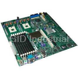


What they say about us
FANTASTIC RESOURCE
One of our top priorities is maintaining our business with precision, and we are constantly looking for affiliates that can help us achieve our goal. With the aid of GID Industrial, our obsolete product management has never been more efficient. They have been a great resource to our company, and have quickly become a go-to supplier on our list!
Bucher Emhart Glass
EXCELLENT SERVICE
With our strict fundamentals and high expectations, we were surprised when we came across GID Industrial and their competitive pricing. When we approached them with our issue, they were incredibly confident in being able to provide us with a seamless solution at the best price for us. GID Industrial quickly understood our needs and provided us with excellent service, as well as fully tested product to ensure what we received would be the right fit for our company.
Fuji
HARD TO FIND A BETTER PROVIDER
Our company provides services to aid in the manufacture of technological products, such as semiconductors and flat panel displays, and often searching for distributors of obsolete product we require can waste time and money. Finding GID Industrial proved to be a great asset to our company, with cost effective solutions and superior knowledge on all of their materials, it’d be hard to find a better provider of obsolete or hard to find products.
Applied Materials
CONSISTENTLY DELIVERS QUALITY SOLUTIONS
Over the years, the equipment used in our company becomes discontinued, but they’re still of great use to us and our customers. Once these products are no longer available through the manufacturer, finding a reliable, quick supplier is a necessity, and luckily for us, GID Industrial has provided the most trustworthy, quality solutions to our obsolete component needs.
Nidec Vamco
TERRIFIC RESOURCE
This company has been a terrific help to us (I work for Trican Well Service) in sourcing the Micron Ram Memory we needed for our Siemens computers. Great service! And great pricing! I know when the product is shipping and when it will arrive, all the way through the ordering process.
Trican Well Service
GO TO SOURCE
When I can't find an obsolete part, I first call GID and they'll come up with my parts every time. Great customer service and follow up as well. Scott emails me from time to time to touch base and see if we're having trouble finding something.....which is often with our 25 yr old equipment.
ConAgra Foods