

 Manufacturers
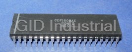
HARRIS SEMICONDUCTOR CDP1802AE
Description
Harris Semiconductor CDP1802AE Microprocessors-CMOS 8-Bit Microprocessor
Part Number
CDP1802AE
Price
Request Quote
Manufacturer
HARRIS SEMICONDUCTOR
Lead Time
Request Quote
Category
PRODUCTS - C
Features
- 16 x 16 Matrix of Registers for Use as Multiple
- 8-Bit Parallel Organization With Bidirectional Data Bus and Multiplexed Address Bus
- Any Combination of Standard RAM and ROM Up to 65,536 Bytes
- On-Chip DMA, Interrupt, and Flag Inputs
- Program Counters, Data Pointers, or Data Registers
- Programmable Single-Bit Output Port
Datasheet

Extracted Text
CDP1802A, CDP1802AC, SEMICONDUCT OR CDP1802BC March 1997 CMOS 8-Bit Microprocessors Features Description • Maximum Input Clock Maximum Frequency Options The CDP1802 family of CMOS microprocessors are 8-bit At V = 5V register oriented central processing units (CPUs) designed DD for use as general purpose computing or control elements in - CDP1802A, AC . . . . . . . . . . . . . . . . . . . . . . . . . 3.2MHz a wide range of stored program systems or products. - CDP1802BC. . . . . . . . . . . . . . . . . . . . . . . . . . . . 5.0MHz • Maximum Input Clock Maximum Frequency Options The CDP1802 types include all of the circuits required for At V = 10V fetching, interpreting, and executing instructions which have DD been stored in standard types of memories. Extensive - CDP1802A, AC . . . . . . . . . . . . . . . . . . . . . . . . . 6.4MHz input/output (I/O) control features are also provided to facili- • Minimum Instruction Fetch-Execute Times tate system design. At V = 5V DD - CDP1802A, AC . . . . . . . . . . . . . . . . . . . . . . . . . . 5.0μs The 1800 series architecture is designed with emphasis on the total microcomputer system as an integral entity so that - CDP1802BC. . . . . . . . . . . . . . . . . . . . . . . . . . . . . 3.2μs systems having maximum flexibility and minimum cost can • Any Combination of Standard RAM and ROM Up to be realized. The 1800 series CPU also provides a synchro- 65,536 Bytes nous interface to memories and external controllers for I/O devices, and minimizes the cost of interface controllers. Fur- •8-Bit Parallel Organization With Bidirectional Data Bus ther, the I/O interface is capable of supporting devices oper- and Multiplexed Address Bus ating in polled, interrupt driven, or direct memory access • 16 x 16 Matrix of Registers for Use as Multiple modes. Program Counters, Data Pointers, or Data Registers The CDP1802A and CDP1802AC have a maximum input •On-Chip DMA, Interrupt, and Flag Inputs clock frequency of 3.2MHz at V = 5V. The CDP1802A and DD CDP1802AC are functionally identical. They differ in that the -Bit Output Port • Programmable Single CDP1802A has a recommended operating voltage range of -to-Use Instructions • 91 Easy 4V to 10.5V, and the CDP1802AC a recommended operat- ing voltage range of 4V to 6.5V. The CDP1802BC is a higher speed version of the CDP1802AC, having a maximum input clock frequency of 5.0MHz at V = 5V, and a recommended operating voltage DD range of 4V to 6.5V. Ordering Information PART NUMBER 5V - 3.2MHz 5V - 5MHz TEMPERATURE RANGE PACKAGE PKG. NO. o o CDP1802ACE CDP1802BCE -40 C to +85 C PDIP E40.6 CDP1802ACEX CDP1802BCEX Burn-In E40.6 o o CDP1802ACQ CDP1802BCQ -40 C to +85 C PLCC N44.65 o o CDP1802ACD - -40 C to +85 C SBDIP D40.6 CDP1802ACDX CDP1802BCDX Burn-In D40.6 CAUTION: These devices are sensitive to electrostatic discharge. Users should follow proper IC Handling Procedures. 1305.2 File Number Copyright © Harris Corporation 1997 3-3 CDP1802A, CDP1802AC, CDP1802BC Pinouts 40 LEAD PDIP (PACKAGE SUFFIX E) 44 LEAD PLCC 40 LEAD SBDIP (PACKAGE SUFFIX D) (PACKAGE TYPE Q) TOP VIEW TOP VIEW CLOCK 1 40 V DD WAIT 2 39 XTAL CLEAR 3 38 DMA IN Q 4 37 DMA OUT SC1 5 36 INTERRUPT SC0 6 35 MWR 6 5 4 3 2 1 44 43 42 41 40 MRD 7 34 TPA SC0 7 39 MWR BUS 7 8 33 TPB MRD 8 38 TPA BUS 6 9 32 MA7 BUS 7 9 37 TPB BUS 5 10 31 MA6 BUS 6 10 36 MA7 BUS 4 11 30 MA5 BUS 5 11 MA6 35 BUS 3 12 29 MA4 NC 12 NC 34 BUS 2 13 28 MA3 BUS 4 13 MA5 33 BUS 3 14 MA4 32 BUS 1 14 27 MA2 BUS 2 15 MA3 31 BUS 0 15 26 MA1 16 BUS 1 MA2 30 V 16 25 MA0 CC BUS 0 17 MA1 29 N2 17 24 EF1 18 19 20 21 22 23 24 25 26 27 28 N1 18 23 EF2 N0 19 22 EF3 V 20 21 EF4 SS ADDRESS BUS CDP1852 INPUT PORT CS2 MA0-7 MA0-7 MA0-4 N0 CS1 MRD MRD MRD CDP1833 CDP1824 CDP1802 1K-ROM 32 BYTE RAM 8-BIT CPU MWR MWR CS TPA TPA CEO N1 DATA CS1 TPB DATA DATA CDP1852 CS2 OUTPUT PORT CLOCK FIGURE 1. TYPICAL CDP1802 SMALL MICROPROCESSOR SYSTEM 3-4 V CC SC1 N2 Q N1 CLEAR N0 WAIT V SS CLOCK NC NC EF4 V DD EF3 XTAL EF2 DMA-IN EF1 DMA-OUT MA0 INTERRUPT CDP1802A, CDP1802AC, CDP1802BC Block Diagram I/O REQUESTS MEMORY ADDRESS LINES I/O FLAGS DMA CONTROL OUT MA6 MA4 MA2 MA0 EF1 EF3 CLEAR DMA EF2 EF4 IN INT WAIT MA7 MA5 MA3 MA1 MUX CLOCK CLOCK LOGIC XTAL SCO STATE CODES SCI CONTROL AND Q LOGIC TIMING LOGIC TPA TPB SYSTEM TIMING MWR MRD TO INSTRUCTION DECODE A REGISTER R(0).1 R(0).0 ARRAY B R(1).1 R(1).0 R ALU INCR/ R(2).1 R(2).0 DECR DF N0 LATCH I/O R(9).1 R(9).0 AND XTP I N N1 COMMANDS R(A).1 R(A).0 DECODE N2 D R(E).1 R(E).0 R(F).1 R(F).0 BUS 0 BUS 1 8-BIT BIDIRECTIONAL DATA BUS BUS 2 BUS 3 BUS 4 BUS 5 BUS 6 BUS 7 FIGURE 2. 3-5 CDP1802A, CDP1802AC, CDP1802BC Absolute Maximum Ratings Thermal Information o o DC Supply Voltage Range, (V ) Thermal Resistance (Typical, Note 4) θ ( C/W) θ ( C/W) DD JA JC (All Voltages Referenced to V Terminal) SS PDIP . . . . . . . . . . . . . . . . . . . . . . . . . . 50 N/A CDP1802A. . . . . . . . . . . . . . . . . . . . . . . . . . . . . . . . . -0.5V to +11V PLCC . . . . . . . . . . . . . . . . . . . . . . . . . . 46 N/A CDP1802AC, CDP1802BC. . . . . . . . . . . . . . . . . . . . -0.5V to +7V SBDIP . . . . . . . . . . . . . . . . . . . . . . . . . 55 15 Input Voltage Range, All Inputs . . . . . . . . . . . . . .-0.5V to V +0.5V DD Device Dissipation Per Output Transistor DC Input Current, any One Input. . . . . . . . . . . . . . . . . . . . . . . . .±10mA T = Full Package Temperature Range . . . . . . . . . . . . . . . 100mW A Operating Temperature Range (T ) A o o Package Type D . . . . . . . . . . . . . . . . . . . . . . . . . . -55 C to +125 C o o Package Type E and Q . . . . . . . . . . . . . . . . . . . . . . -40 C to +85 C o o Storage Temperature Range (T ) . . . . . . . . . . . . -65 C to +150 C STG Lead Temperature (During Soldering) At distance 1/16 ± 1/32 In. (1.59 ± 0.79mm) o from case for 10s max . . . . . . . . . . . . . . . . . . . . . . . . . . . +265 C o Lead Tips Only . . . . . . . . . . . . . . . . . . . . . . . . . . . . . . . . . +300 C CAUTION: Stresses above those listed in “Absolute Maximum Ratings” may cause permanent damage to the device. This is a stress only rating and operation of the device at these or any other conditions above those indicated in the operational sections of this specification is not implied. o o Recommended Operating Conditions T = -40 C to +85 C. For maximum reliability, operating conditions should be selected so A that operation is always within the following ranges: TEST CONDITIONS CDP1802A CDP1802AC CDP1802BC (NOTE 2) V V CC DD PARAMETER (V) (V) MIN MAX MIN MAX MIN MAX UNITS DC Operating Voltage Range - - 4 10.5 4 6.5 4 6.5 V Input Voltage Range - - V V V V V V V SS DD SS DD SS DD Maximum Clock Input Rise or 4 to 6.5 4 to 6.5 - - - 1 - 1 μs Fall Time 4 to 10.5 4 to 10.5 - 1 ---- μs Minimum Instruction Time 5 5 5-5- 3.2 - μs (Note 3) 5 10 4 ----- μs 10 10 2.5 ----- μs Maximum DMA Transfer Rate 5 5 - 400 - 400 - 667 KBytes/s 5 10 - 500 ---- 10 10 - 800 ---- Maximum Clock Input Frequency, 5 5 DC 3.2 DC 3.2 DC 5 MHz f , Load Capacitance CL 5 10 DC 4 ---- MHz (C ) = 50pF L 10 10 DC 6.4 ---- MHz NOTES: 1. Printed circuit board mount: 57mm x 57mm minimum area x 1.6mm thick G10 epoxy glass, or equivalent. 2. V must never exceed V . CC DD 3. Equals 2 machine cycles - one Fetch and one Execute operation for all instructions except Long Branch and Long Skip, which require 3 machine cycles - one Fetch and two Execute operations. 4. θ is measured with component mounted on an evaluation board in free air. JA 3-6 CDP1802A, CDP1802AC, CDP1802BC o o Static Electrical Specifications at T = -40 C to +85 C, Except as Noted A CDP1802AC, TEST CONDITIONS CDP1802A CDP1802BC V , CC V V V (NOTE 1) (NOTE 1) OUT IN DD PARAMETER SYMBOL (V) (V) (V) MIN TYP MAX MIN TYP MAX UNITS Quiescent Device Current I - - 5 - 0.1 50 - 1 200 μA DD - - 10 - 1 200 - - - μA Output Low Drive (Sink) Current I 0.4 0, 5 5 1.1 2.2 - 1.1 2.2 - mA OL (Except XTAL) 0.5 0, 10 10 2.2 4.4 - - - - mA XTAL 0.4 5 5 170 350 - 170 350 - μA Output High Drive (Source) Current I 4.6 0, 5 5 -0.27 -0.55 - -0.27 -0.55 - mA OH (Except XTAL) 9.5 0, 10 10 -0.55 -1.1 - - - - mA XTAL 4.6 0 5 -125 -250 - -125 -250 - μA Output Voltage - 0, 5 5 - 0 0.1 - 0 0.1 V Low Level V - 0, 10 10 - 0 0.1 - - - V OL Output Voltage - 0, 5 5 4.9 5 - 4.9 5 - V High Level V - 0, 10 10 9.9 10 - - - - V OH Input Low Voltage V 0.5, 4.5 - 5 - - 1.5 - - 1.5 V IL 0.5, 4.5 - 5, 10 - - 1 - - - V 1, 9 - 10 - - 3 - - - V Input High Voltage V 0.5, 4.5 - 5 3.5 - - 3.5 - - V IH 0.5, 4.5 - 5, 10 4 - - - - - V 1, 9 - 10 7 - - - - - V CLEAR Input Voltage V - - 5 0.4 0.5 - 0.4 0.5 - V H Schmitt Hysteresis - - 5, 10 0.3 0.4 - - - - V - - 10 1.5 2 - - - - V -4 -4 Input Leakage Current I Any 0, 5 5 - ±10 ±1- ±10 ±1 μA IN Input -4 0, 10 10 - ±10 ±1- - - μA -4 -4 Three-State Output Leakage I 0, 5 0, 5 5 - ±10 ±1- ±10 ±1 μA OUT -4 Current 0, 10 0, 10 10 - ±10 ±1- - - μA Operating Current CDP1802A, AC I -- 5 - 2 4 - 2 4 mA DDI at f = 3.2MHz (Note 2) CDP1802BC -- 5 - - - - 3 6 mA at f = 5.0MHz Minimum Data Retention V V = V - 2 2.4 - 2 2.4 V DR DD DR Voltage Data Retention Current I V = 2.4V - 0.05 - - 0.5 - μA DR DD 3-7 CDP1802A, CDP1802AC, CDP1802BC o o Static Electrical Specifications at T = -40 C to +85 C, Except as Noted (Continued) A CDP1802AC, TEST CONDITIONS CDP1802A CDP1802BC V , CC V V V (NOTE 1) (NOTE 1) OUT IN DD PARAMETER SYMBOL (V) (V) (V) MIN TYP MAX MIN TYP MAX UNITS Input Capacitance C - 5 7.5 - 5 7.5 pF IN Output Capacitance C - 10 15 - 10 15 pF OUT NOTES: o 1. Typical values are for T = +25 C and nominal V . A DD 2. Idle “00” at M(0000), C = 50pF. L o o Dynamic Electrical Specifications T = -40 C to +85 C, C = 50pF, V ±5%, Except as Noted A L DD TEST CDP1802A, CONDITIONS CDP1802AC CDP1802BC (NOTE 1) (NOTE 1) PARAMETER SYMBOL V (V) V (V) TYP MAX TYP MAX UNITS CC DD PROPAGATION DELAY TIMES Clock to TPA, TPB t , t 5 5 200 300 200 300 ns PLH PHL 5 10 150 250 - - ns 10 10 100 150 - - ns Clock-to-Memory High-Address Byte t , t 5 5 600 850 475 525 ns PLH PHL 5 10 400 600 - - ns 10 10 300 400 - - ns Clock-to-Memory Low-Address Byte Valid t , t 5 5 250 350 175 250 ns PLH PHL 5 10 150 250 - - ns 10 10 100 150 - - ns Clock to MRD t 5 5 200 300 175 275 ns PHL 5 10 150 250 - - ns 10 10 100 150 - - ns Clock to MRD t 5 5 200 350 175 275 ns PLH 5 10 150 290 - - ns 10 10 100 175 - - ns Clock to MWR t , t 5 5 200 300 175 225 ns PLH PHL 5 10 150 250 - - ns 10 10 100 150 - - ns Clock to (CPU DATA to BUS) Valid t , t 5 5 300 450 250 375 ns PLH PHL 5 10 250 350 - - ns 10 10 100 200 - - ns 3-8 CDP1802A, CDP1802AC, CDP1802BC o o Dynamic Electrical Specifications T = -40 C to +85 C, C = 50pF, V ±5%, Except as Noted (Continued) A L DD TEST CDP1802A, CONDITIONS CDP1802AC CDP1802BC (NOTE 1) (NOTE 1) PARAMETER SYMBOL V (V) V (V) TYP MAX TYP MAX UNITS CC DD Clock to State Code t , t 5 5 300 450 250 400 ns PLH PHL 5 10 250 350 - - ns 10 10 150 250 - - ns Clock to Q t , t 5 5 250 400 200 300 ns PLH PHL 5 10 150 250 - - ns 10 10 100 150 - - ns Clock to N (0 - 2) t , t 5 5 300 550 275 350 ns PLH PHL 5 10 200 350 - - ns 10 10 150 250 - - ns MINIMUM SET UP AND HOLD TIMES Data Bus Input Set Up t 5 5 -20 25 -20 0 ns SU 5 10 0 50 - - ns 10 10 -10 40 - - ns Data Bus Input Hold t 5 5 150 200 125 150 ns H (Note 2) 5 10 100 125 - - ns 10 10 75 100 - - ns DMA Set Up t 5 5 0 30 0 30 ns SU 5 10 0 20 - - ns 10 10 0 10 - - ns DMA Hold t 5 5 150 250 100 150 ns H (Note 2) 5 10 100 200 - - ns 10 10 75 125 - - ns Interrupt Set Up t 5 5 -75 0 -75 0 ns SU 5 10 -50 0 - - ns 10 10 -25 0 - - ns Interrupt Hold t 5 5 100 150 75 125 ns H (Note 2) 5 10 75 100 - - ns 10 10 50 75 - - ns WAIT Set Up t 5 5 10 50 20 40 ns SU 5 10 -10 15 - - ns 10 10 0 25 - - ns 3-9 CDP1802A, CDP1802AC, CDP1802BC o o Dynamic Electrical Specifications T = -40 C to +85 C, C = 50pF, V ±5%, Except as Noted (Continued) A L DD TEST CDP1802A, CONDITIONS CDP1802AC CDP1802BC (NOTE 1) (NOTE 1) PARAMETER SYMBOL V (V) V (V) TYP MAX TYP MAX UNITS CC DD EF1-4 Set Up t 5 5 -30 20 -30 0 ns SU 5 10 -20 30 - - ns 10 10 -10 40 - - ns EF1-4 Hold t 5 5 150 200 100 150 ns H (Note 2) 5 10 100 150 - - ns 10 10 75 100 - - ns Minimum Pulse Width Times CLEAR Pulse Width t 5 5 150 300 100 150 ns WL (Note 2) 5 10 100 200 - - ns 10 10 75 150 - - ns CLOCK Pulse Width t 5 5 125 150 90 100 ns WL 5 10 100 125 - - ns 10 10 60 75 - - ns NOTES: o 1. Typical values are for T = +25 C and nominal V . A DD 2. Maximum limits of minimum characteristics are the values above which all devices function. o Timing Specifications as a function of T(T = 1/f ) at T = -40 to +85 C, Except as Noted CLOCK A CDP1802A, TEST CONDITIONS CDP1802AC CDP1802BC (NOTE 1) (NOTE 1) PARAMETERS SYMBOL V (V) V (V) MIN TYP MIN TYP UNITS CC DD High-Order Memory-Address Byte t 5 5 2T-550 2T-400 2T-325 2T-275 ns SU Set Up to TPA Time 5 10 2T-350 2T250 - - ns 10 10 2T-250 2T-200 - - ns High-Order Memory-Address Byte t 5 5 t/2-25 T/2-15 T/2-25 T/2-15 ns H Hold After TPA Time 5 10 T/2-35 T/2-25 - - ns 10 10 T/2-10 T/2-+0 - - ns Low-Order Memory-Address Byte t 5 5 T-30 T+0 T-30 T+0 ns H Hold After WR Time 5 10 T-20 T+0 - - ns 10 10 T-10 T+0 - - ns CPU Data to Bus Hold After WR t 5 5 T-200 T-150 T-175 T-125 ns H Time 5 10 T-150 T-100 - - ns 10 10 T-100 T-50 - - ns 3-10 CDP1802A, CDP1802AC, CDP1802BC o Timing Specifications as a function of T(T = 1/f ) at T = -40 to +85 C, Except as Noted CLOCK A CDP1802A, TEST CONDITIONS CDP1802AC CDP1802BC (NOTE 1) (NOTE 1) PARAMETERS SYMBOL V (V) V (V) MIN TYP MIN TYP UNITS CC DD Required Memory Access Time t 5 5 5T-375 5T-250 5T-225 5T-175 ns ACC Address to Data 5 10 5T-250 5T-150 - - ns 10 10 5T-190 5T-100 - - ns MRD to TPA t 5 5 T/2-25 T/2-18 T/2-20 T/2-15 ns SU 5 10 T/2-20 T/2-15 - - ns 10 10 T/2-15 T/2-10 - - ns NOTE: o 1. Typical values are for T = +25 C and nominal V . A DD Timing Waveforms FETCH (READ) EXECUTE (WRITE) 00 01 10 11 20 21 30 31 40 41 50 51 60 61 70 71 00 01 10 11 20 21 30 31 40 41 50 51 60 61 70 71 00 CLOCK HI BYTE LOW BYTE HI BYTE LOW BYTE ADDRESS TPA TPB MRD MWR DATA VALID INPUT DATA VALID OUTPUT DATA FIGURE 3. BASIC DC TIMING WAVEFORM, ONE INSTRUCTION CYCLE 3-11 CDP1802A, CDP1802AC, CDP1802BC Timing Waveforms (Continued) 0 1 2 3 4 5 6 7 0 t W CLOCK 00 01 10 11 20 21 30 31 40 41 50 51 60 61 70 71 00 01 t t PLH PHL TPA t t PLH PHL TPB t t SU H t , t PLH PHL t , t t , t MEMORY HIGH ORDER PLH PHL LOW ORDER PLH PHL ADDRESS ADDRESS BYTE ADDRESS BYTE t H MRD t t t PLH PHL SU t (MEMORY PLH READ CYCLE) MWR t t PHL PLH t PLH (MEMORY t PHL WRITE CYCLE) t H t , t DATA FROM PLH PHL CPU TO BUS t t , t PLH STATE PLH PHL CODES t PHL t , t PLH PHL Q t N0, N1, N2 PLH (I/O EXECUTION t PLH CYCLE) DATA LATCHED IN CPU t t DATA FROM SU H BUS TO CPU DMA SAMPLED (S1, S2, S3) t t SU H DMA REQUEST INTERRUPT SAMPLED (S1, S2) t t SU H INTERRUPT FLAG LINES REQUEST SAMPLED (IN S1) t t SU H EF 1-4 t SU ANY NEGATIVE WAIT TRANSITION t W CLEAR NOTES: 1. This timing diagram is used to show signal relationships only and does not represent any specific machine cycle. 2. All measurements are referenced to 50% point of the waveforms. 3. Shaded areas indicate “Don’t Care” or undefined state. Multiple transitions may occur during this period. FIGURE 4. TIMING WAVEFORM 3-12 CDP1802A, CDP1802AC, CDP1802BC Machine Cycle Timing Waveforms (Propagation Delays Not Shown) 01 2 3 45 6 7 01 2 3 45 6 701 2 3 45 6 7 0 CLOCK TPA TPB MACHINE CYCLE n CYCLE (n + 1) CYCLE (n + 2) CYCLE MA HIGH ADD LOW ADDRESS HIGH ADD LOW ADDRESS HIGH ADD LOW ADDRESS FIGURE 5. GENERAL TIMING WAVEFORMS INSTRUCTION EXECUTE FETCH (S0) EXECUTE (S1) FETCH (S0) MEMORY READ CYCLE NON MEMORY CYCLE MEMORY READ CYCLE MRD MWR (HIGH) MEMORY OUTPUT VALID OUTPUT VALID ALLOWABLE MEMORY ACCESS OUTPUT “DON’T CARE” OR INTERNAL DELAYS HIGH IMPEDANCE STATE FIGURE 6. NON-MEMORY CYCLE TIMING WAVEFORMS INSTRUCTION FETCH (S0) EXECUTE (S1) FETCH (S0) EXECUTE MEMORY READ CYCLE MEMORY WRITE CYCLE MEMORY READ CYCLE MRD MWR MEMORY OUTPUT VALID OUTPUT VALID ALLOWABLE MEMORY ACCESS OUTPUT CPU OUTPUT OFF VALID DATA OFF VALID TO MEMORY “DON’T CARE” OR INTERNAL DELAYS HIGH IMPEDANCE STATE FIGURE 7. MEMORY WRITE CYCLE TIMING WAVEFORMS 3-13 CDP1802A, CDP1802AC, CDP1802BC Machine Cycle Timing Waveforms (Propagation Delays Not Shown) (Continued) INSTRUCTION FETCH (S0) EXECUTE (S1) FETCH (S0) EXECUTE MEMORY READ CYCLE MEMORY READ CYCLE MEMORY READ CYCLE MRD MWR (HIGH) MEMORY OUTPUT VALID VALID VALID OUTPUT ALLOWABLE MEMORY ACCESS OUTPUT OUTPUT “DON’T CARE” OR INTERNAL DELAYS HIGH IMPEDANCE STATE FIGURE 8. MEMORY READ CYCLE TIMING WAVEFORMS INSTRUCTION FETCH (S0) EXECUTE (S1) EXECUTE (S1) FETCH (S0) MEMORY READ CYCLE MEMORY READ CYCLE MEMORY READ CYCLE MRD MWR (HIGH) MEMORY OUTPUT VALID VALID OUTPUT VALID OUTPUT ALLOWABLE MEMORY ACCESS OUTPUT “DON’T CARE” OR INTERNAL DELAYS HIGH IMPEDANCE STATE FIGURE 9. LONG BRANCH OR LONG SKIP CYCLE TIMING WAVEFORMS 3-14 CDP1802A, CDP1802AC, CDP1802BC Machine Cycle Timing Waveforms (Propagation Delays Not Shown) (Continued) 01 2 3 45 6 7 01 2 3 45 6 7 0 CLOCK TPA TPB MACHINE CYCLE n CYCLE (n + 1) CYCLE INSTRUCTION FETCH (S0) EXECUTE (S1) MRD N0 - N2 N = 9 - F MWR MEMORY OUTPUT VALID OUTPUT ALLOWABLE MEMORY ACCESS DATA VALID DATA FROM INPUT DEVICE BUS (NOTE 1) MEMORY READ CYCLE MEMORY WRITE CYCLE NOTE 1 HIGH IMPEDANCE STATE “DON’T CARE” OR INTERNAL DELAYS USER GENERATED SIGNAL FIGURE 10. INPUT CYCLE TIMING WAVEFORMS 01 2 3 45 6 7 01 2 3 45 6 7 0 CLOCK TPA TPB MACHINE CYCLE n CYCLE (n + 1) CYCLE INSTRUCTION FETCH (S0) EXECUTE (S1) MRD N = 1 - 9 N0 - N2 ALLOWABLE MEMORY ACCESS DATA BUS VALID OUTPUT ALLOWABLE MEMORY ACCESS VALID DATA FROM MEMORY DATA STROBE (MRD • TPB • N) MEMORY READ CYCLE MEMORY READ CYCLE (NOTE 1) NOTE 1 “DON’T CARE” OR INTERNAL DELAYS HIGH IMPEDANCE STATE USER GENERATED SIGNAL FIGURE 11. OUTPUT CYCLE TIMING WAVEFORMS 3-15 CDP1802A, CDP1802AC, CDP1802BC Machine Cycle Timing Waveforms (Propagation Delays Not Shown) (Continued) 01 2 3 45 6 7 01 2 3 45 6 7 01 2 3 45 67 CLOCK TPA TPB MACHINE CYCLE n CYCLE (n+1) CYCLE (n+2) CYCLE INSTRUCTION FETCH (S0) EXECUTE (S1) DMA (S2) DMA-IN MRD MWR MEMORY OUTPUT VALID OUTPUT VALID DATA FROM INPUT DEVICE DATA BUS (NOTE 1) MEMORY READ CYCLE MEMORY READ, WRITE MEMORY WRITE CYCLE OR NON-MEMORY CYCLE NOTE 1 “DON’T CARE” OR INTERNAL DELAYS HIGH IMPEDANCE STATE USER GENERATED SIGNAL FIGURE 12. DMA IN CYCLE TIMING WAVEFORMS 01234567012345670123456 CLOCK TPA TPB MACHINE CYCLE n CYCLE (n + 1) CYCLE (n + 2) CYCLE INSTRUCTION FETCH (S0) EXECUTE (S1) DMA (S2) DMA OUT (NOTE 1) MRD MWR MEMORY OUTPUT VALID OUTPUT VALID DATA FROM MEMORY DATA STROBE (S2 • TPB) MEMORY READ CYCLE MEMORY READ, WRITE MEMORY READ CYCLE (NOTE 1) OR NON-MEMORY CYCLE NOTE 1 “DON’T CARE” OR INTERNAL DELAYS HIGH IMPEDANCE STATE USER GENERATED SIGNAL FIGURE 13. DMA OUT CYCLE TIMING WAVEFORMS 3-16 CDP1802A, CDP1802AC, CDP1802BC Machine Cycle Timing Waveforms (Propagation Delays Not Shown) (Continued) 01234567012345670123456 CLOCK TPA TPB MACHINE CYCLE n CYCLE (n + 1) CYCLE (n + 2) CYCLE INSTRUCTION FETCH (S0) EXECUTE (S1) INTERRUPT (S3) MRD MWR INTERRUPT (NOTE 1) (INTERNAL) IE MEMORY OUTPUT VALID OUTPUT MEMORY READ, WRITE MEMORY READ CYCLE NON-MEMORY CYCLE OR NON-MEMORY CYCLE NOTE 1 “DON’T CARE” OR INTERNAL DELAYS HIGH IMPEDANCE STATE USER GENERATED SIGNAL FIGURE 14. INTERRUPT CYCLE TIMING WAVEFORMS Performance Curves 8 8 C , LOAD CAPACITANCE = 50pF L C , LOAD CAPACITANCE = 50pF L 7 7 V = V = 10V CC DD 6 6 5 5 V = 5V, V = 10V CC DD V = V = 5V 4 CC DD 4 V = V = 5V 3 CC DD 3 2 2 1 1 0 0 25 35 45 55 65 75 85 95 105 115 125 25 35 45 55 65 75 85 95 105 115 125 o T , AMBIENT TEMPERATURE ( C) A o T , AMBIENT TEMPERATURE ( C) A FIGURE 15. CDP1802A, AC TYPICAL MAXIMUM CLOCK FIGURE 16. CDP1802BC TYPICAL MAXIMUM CLOCK FREQUENCY AS A FUNCTION OF TEMPERATURE FREQUENCY AS A FUNCTION OF TEMPERATURE 3-17 f , SYSTEM MAXIMUM CLOCK CL FREQUENCY (MHz) f , SYSTEM MAXIMUM CLOCK CL FREQUENCY (MHz) CDP1802A, CDP1802AC, CDP1802BC Performance Curves (Continued) V , DRAIN-TO-SOURCE VOLTAGE (V) DS 400 -10 -9 -8 -7 -6 -5 -4 -3 -2 -1 0 o T = 25 C V = V = 5V A CC DD 350 V , GATE-TO-VOLTAGE = -5V GS 1 300 2 250 3 V = V = 10V CC DD 200 -10V 4 t 150 TLH V = V = 5V 5 CC DD 100 t THL 6 50 V = V = 10V CC DD 7 0 o o T , AMBIENT TEMPERATURE = -40 C TO +85 C 0 25 50 75 100 125 150 175 200 A C , LOAD CAPACITANCE (pF) L FIGURE 17. TYPICAL TRANSITION TIME vs LOAD CAPACI- FIGURE 18. CDP1802A, AC MINIMUM OUTPUT HIGH (SOURCE) TANCE FOR ALL TYPES CURRENT CHARACTERISTICS V , DRAIN-TO-SOURCE VOLTAGE (V) DS o o T = -40 C TO +85 C -5 -4 -3 -2 -1 0 A 35 30 1 25 V , GATE-TO-SOURCE = 10V GS 20 V , GATE-TO-VOLTAGE = -5V GS 2 15 10 5V 3 5 012345678910 4 V , DRAIN-TO-SOURCE VOLTAGE (V) DS FIGURE 19. CDP1802A, AC MINIMUM OUTPUT LOW (SINK) FIGURE 20. CDP1802BC MINIMUM OUTPUT HIGH (SOURCE) CURRENT CHARACTERISTICS CURRENT CHARACTERISTICS 150 o o T = -40 C TO +85 C A o T = 25 C A V = V = 5V CC DD 125 20 100 Δt PLH 75 10 V = V = 10V CC DD Δt 50 PHL V , GATE-TO-SOURCE = 5V GS V = V = 5V CC DD 5 25 V = V = 10V CC DD 0 25 50 100 150 200 012345 ΔC , Δ LOAD CAPACITANCE (pF) L V , DRAIN-TO-SOURCE VOLTAGE (V) DS NOTE: ANY OUTPUT EXCEPT XTAL FIGURE 21. CDP1802BC MINIMUM OUTPUT LOW (SINK) FIGURE 22. TYPICAL CHANGE IN PROPAGATION DELAY AS A CURRENT CHARACTERISTICS FUNCTION OF A CHANGE IN LOAD CAPACITANCE FOR ALL TYPES 3-18 I , OUTPUT LOW (SINK) CURRENT (mA) I , OUTPUT LOW (SINK) CURRENT (mA) t t , TRANSITION TIME (ns) OL OL THL, TLH Δt , Δt , Δ PROPAGATION DELAY PLH PHL TIME (ns) I , OUTPUT HIGH (SOURCE) CURRENT (mA) I , OUTPUT HIGH (SOURCE) CURRENT (mA) OH OH CDP1802A, CDP1802AC, CDP1802BC Performance Curves (Continued) 1000 o T = 25 C A V = V = 10V CC DD 100 BRANCH 10 IDLE 1 V = V = 5V CC DD 0.1 0.01 0.1 1 10 f , CLOCK INPUT FREQUENCY (MHz) CL NOTE: IDLE = “00” AT M(0000), BRANCH = “3707” AT M(8107), CL = 50pF FIGURE 23. TYPICAL POWER DISSIPATION AS A FUNCTION OF CLOCK FREQUENCY FOR BRANCH INSTRUCTION AND IDLE INSTRUCTION FOR ALL TYPES Signal Descriptions Bus 0 to Bus 7 (Data Bus) Interrupt Action - X and P are stored in T after executing current instruction; designator X is set to 2; designator P is 8-bit bidirectional DATA BUS lines. These lines are used for set to 1; interrupt enable is reset to 0 (inhibit); and instruction transferring data between the memory, the microprocessor, execution is resumed. The interrupt action requires one and I/O devices. machine cycle (S3). N0 to N2 (I/O Control Lines) DMA Action - Finish executing current instruction; R(0) points to memory area for data transfer; data is loaded into Activated by an I/O instruction to signal the I/O control logic of or read out of memory; and increment R(0). a data transfer between memory and I/O interface. These lines can be used to issue command codes or device selec- NOTE: In the event of concurrent DMA and Interrupt requests, tion codes to the I/O devices (independently or combined with DMA-lN has priority followed by DMA-OUT and then Interrupt. the memory byte on the data bus when an I/O instruction is SC0, SC1, (2 State Code Lines) being executed). The N bits are low at all times except when an I/O instruction is being executed. During this time their These outputs indicate that the CPU is: 1) fetching an state is the same as the corresponding bits in the N register. instruction, or 2) executing an instruction, or 3) processing a DMA request, or 4) acknowledging an interrupt request. The The direction of data flow is defined in the I/O instruction by bit levels of state code are tabulated below. All states are valid N3 (internally) and is indicated by the level of the MRD signal. at TPA. H = V , L = V . CC SS MRD = V : Data from I/O to CPU and Memory CC STATE CODE LINES MRD = V : Data from Memory to I/O SS STATE TYPE SC1 SC0 EF1 to EF4 (4 Flags) S0 (Fetch) L L These inputs enable the I/O controllers to transfer status information to the processor. The levels can be tested by the S1 (Execute) L H conditional branch instructions. They can be used in con- S2 (DMA) H L junction with the INTERRUPT request line to establish inter- rupt priorities. These flags can also be used by I/O devices S3 (Interrupt) H H to “call the attention” of the processor, in which case the pro- gram must routinely test the status of these flag(s). The TPA, TPB (2 Timing Pulses) flag(s) are sampled at the beginning of every S1 cycle. Positive pulses that occur once in each machine cycle (TPB INTERRUPT, DMA-lN, DMA-OUT (3 I/O Requests) follows TPA). They are used by I/O controllers to interpret codes and to time interaction with the data bus. The trailing These inputs are sampled by the CPU during the interval edge of TPA is used by the memory system to latch the between the leading edge of TPB and the leading edge of higher-order byte of the 16-bit memory address. TPA is sup- TPA. pressed in IDLE when the CPU is in the load mode. 3-19 P , TYPICAL POWER DISSIPATION D FOR CDP1802D (mW) CDP1802A, CDP1802AC, CDP1802BC MA0 to MA7 (8 Memory Address Lines) Architecture In each cycle, the higher-order byte of a 16-bit CPU memory The CPU block diagram is shown in Figure 2. The principal address appears on the memory address lines MA0-7 first. feature of this system is a register array (R) consisting of six- Those bits required by the memory system can be strobed teen 16-bit scratchpad registers. Individual registers in the into external address latches by timing pulse TPA. The low array (R) are designated (selected) by a 4-bit binary code order byte of the 16-bit address appears on the address lines from one of the 4-bit registers labeled N, P and X. The con- after the termination of TPA. Latching of all 8 higher-order tents of any register can be directed to any one of the follow- address bits would permit a memory system of 64K bytes. ing three paths: MWR (Write Pulse) 1. The external memory (multiplexed, higher-order byte first, on to 8 memory address lines). A negative pulse appearing in a memory-write cycle, after the address lines have stabilized. 2. The D register (either of the two bytes can be gated to D). 3. The increment/decrement circuit where it is increased or MRD (Read Level) decreased by one and stored back in the selected 16-bit A low level on MRD indicates a memory read cycle. It can be register. used to control three-state outputs from the addressed mem- The three paths, depending on the nature of the instruction, ory which may have a common data input and output bus. If a may operate independently or in various combinations in the memory does not have a three-state high-impedance output, same machine cycle. MRD is useful for driving memory/bus separator gates. It is also used to indicate the direction of data transfer during an With two exceptions, CPU instruction consists of two 8- I/O instruction. For additional information see Table 1. clock-pulse machine cycles. The first cycle is the fetch cycle, and the second - and third if necessary - are execute cycles. Q During the fetch cycle the four bits in the P designator select one of the 16 registers R(P) as the current program counter. Single bit output from the CPU which can be set or reset The selected register R(P) contains the address of the mem- under program control. During SEQ or REQ instruction exe- ory location from which the instruction is to be fetched. cution, Q is set or reset between the trailing edge of TPA and When the instruction is read out from the memory, the higher the leading edge of TPB. order 4 bits of the instruction byte are loaded into the register CLOCK and the lower order 4 bits into the N register. The content of the program counter is automatically incremented by one so Input for externally generated single-phase clock. The clock is that R(P) is now “pointing” to the next byte in the memory. counted down internally to 8 clock pulses per machine cycle. The X designator selects one of the 16 registers R(X) to XTAL “point” to the memory for an operand (or data) in certain ALU or I/O operations. Connection to be used with clock input terminal, for an exter- nal crystal, if the on-chip oscillator is utilized. The crystal is The N designator can perform the following five functions connected between terminals 1 and 39 (CLOCK and XTAL) depending on the type of instruction fetched: in parallel with a resistance (10MΩ typ). Frequency trimming 1. Designate one of the 16 registers in R to be acted upon capacitors may be required at terminals 1 and 39. For addi- during register operations. tional information, see Application Note AN6565. 2. Indicate to the I/O devices a command code or device WAIT, CLEAR (2 Control Lines) selection code for peripherals. Provide four control modes as listed in the following truth table: 3. Indicate the specific operation to be executed during the ALU instructions, types of test to be performed during the CLEAR WAIT MODE Branch instruction, or the specific operation required in a L L LOAD class of miscellaneous instructions (70 - 73 and 78 - 7B). L H RESET 4. Indicate the value to be loaded into P to designate a new register to be used as the program counter R(P). H L PAUSE 5. Indicate the value to be loaded into X to designate a new H H RUN register to be used as data pointer R(X). V , V , V (Power Levels) DD SS CC The registers in R can be assigned by a programmer in three different ways: as program counters, as data pointers, or as is isolated from the The internal voltage supply V DD scratchpad locations (data registers) to hold two bytes of data. Input/Output voltage supply V so that the processor may CC operate at maximum speed while interfacing with peripheral Program Counters devices operating at lower voltage. V must be less than or CC equal to V . All outputs swing from V to V . The recom- Any register can be the main program counter; the address DD SS CC mended input voltage swing is V to V . of the selected register is held in the P designator. Other reg- SS CC 3-20 CDP1802A, CDP1802AC, CDP1802BC Interrupt Servicing isters in R can be used as subroutine program counters. By single instruction the contents of the P register can be Register R(1) is always used as the program counter when- changed to effect a “call” to a subroutine. When interrupts ever interrupt servicing is initiated. When an interrupt are being serviced, register R(1) is used as the program request occurs and the interrupt is allowed by the program counter for the user's interrupt servicing routine. After reset, (again, nothing takes place until the completion of the cur- and during a DMA operation, R(0) is used as the program rent instruction), the contents of the X and P registers are counter. At all other times the register designated as pro- stored in the temporary register T, and X and P are set to gram counter is at the discretion of the user. new values; hex digit 2 in X and hex digit 1 in P. Interrupt Enable is automatically deactivated to inhibit further inter- Data Pointers rupts. The user's interrupt routine is now in control; the con- The registers in R may be used as data pointers to indicate a tents of T may be saved by means of a single instruction (78) location in memory. The register designated by X (i.e., R(X)) in the memory location pointed to by R(X). At the conclusion points to memory for the following instructions (see Table 1). of the interrupt, the user's routine may restore the pre-inter- rupted value of X and P with a single instruction (70 or 71). 1. ALU operations F1 - F5, F7, 74, 75, 77 The Interrupt Enable flip-flop can be activated to permit fur- 2. Output instructions 61 through 67 ther interrupts or can be disabled to prevent them. 3. Input instructions 69 through 6F CPU Register Summary 4. Certain miscellaneous instructions - 70 - 73, 78, 60, F0 D 8 Bits Data Register (Accumulator) The register designated by N (i.e., R(N)) points to memory DF 1-Bit Data Flag (ALU Carry) for the “load D from memory” instructions 0N and 4N and the B 8 Bits Auxiliary Holding Register “Store D” instruction 5N. The register designated by P (i.e., R 16 Bits 1 of 16 Scratchpad Registers the program counter) is used as the data pointer for ALU instructions F8 - FD, FF, 7C, 7D, 7F. During these instruction P 4 Bits Designates which register is Program Counter executions, the operation is referred to as “data immediate”. X 4 Bits Designates which register is Data Pointer Another important use of R as a data pointer supports the N 4 Bits Holds Low-Order Instruction Digit built-in Direct-Memory-Access (DMA) function. When a I 4 Bits Holds High-Order Instruction Digit DMA-ln or DMA-Out request is received, one machine cycle T 8 Bits Holds old X, P after Interrupt (X is high nibble) is “stolen”. This operation occurs at the end of the execute lE 1-Bit Interrupt Enable machine cycle in the current instruction. Register R(0) is always used as the data pointer during the DMA operation. Q 1-Bit Output Flip-Flop The data is read from (DMA-Out) or written into (DMA-ln) the memory location pointed to by the R(0) register. At the end CDP1802 Control Modes of the transfer, R(0) is incremented by one so that the pro- The WAIT and CLEAR lines provide four control modes as cessor is ready to act upon the next DMA byte transfer listed in the following truth table: request. This feature in the 1800-series architecture saves a substantial amount of logic when fast exchanges of blocks of CLEAR WAIT MODE data are required, such as with magnetic discs or during L L LOAD CRT-display-refresh cycles. L H RESET Data Registers H L PAUSE When registers in R are used to store bytes of data, four H H RUN instructions are provided which allow D to receive from or The function of the modes are defined as follows: write into either the higher-order or lower-order byte portions of the register designated by N. By this mechanism (together Load with loading by data immediate) program pointer and data pointer designations are initialized. Also, this technique Holds the CPU in the IDLE execution state and allows an I/O allows scratchpad registers in R to be used to hold general device to load the memory without the need for a “bootstrap” data. By employing increment or decrement instructions, loader. It modifies the IDLE condition so that DMA-lN opera- such registers may be used as loop counters. tion does not force execution of the next instruction. The Q Flip-Flop Reset An internal flip-flop, Q, can be set or reset by instruction and Registers l, N, Q are reset, lE is set and 0’s (VSS) are placed can be sensed by conditional branch instructions. The output on the data bus. TPA and TPB are suppressed while reset is of Q is also available as a microprocessor output. held and the CPU is placed in S1. The first machine cycle after termination of reset is an initialization cycle which requires 9 clock pulses. During this cycle the CPU remains in S1 and reg- ister X, P, and R(0) are reset. Interrupt and DMA servicing are 3-21 CDP1802A, CDP1802AC, CDP1802BC suppressed during the initialization cycle. The next cycle is an Run-Mode State Transitions S0, S1, or an S2 but never an S3. With the use of a 71 instruc- The CPU state transitions when in the RUN and RESET tion followed by 00 at memory locations 0000 and 0001, this modes are shown in Figure 25. Each machine cycle requires feature may be used to reset IE, so as to preclude interrupts the same period of time, 8 clock pulses, except the initializa- until ready for them. Power-up reset can be realized by con- tion cycle, which requires 9 clock pulses. The execution of necting an RC network directly to the CLEAR pin, since it has a an instruction requires either two or three machine cycles, Schmitt triggered input, see Figure 24. S0 followed by a single S1 cycle or two S1 cycles. S2 is the V CC response to a DMA request and S3 is the interrupt response. Table 2 shows the conditions on Data Bus and Memory CDP1802 R S Address lines during all machine states. THE RC TIME CONSTANT SHOULD BE GREATER THAN CLEAR THE OSCILLATOR START-UP Instruction Set 3 TIME (TYPICALLY 20ms) C The CPU instruction summary is given in Table 1. Hexadeci- mal notation is used to refer to the 4-bit binary codes. FIGURE 24. RESET DIAGRAM In all registers bits are numbered from the least significant bit (LSB) to the most significant bit (MSB) starting with 0. Pause R(W): Register designated by W, where Stops the internal CPU timing generator on the first negative W = N or X, or P high-to-low transition of the input clock. The oscillator contin- R(W).0: Lower order byte of R(W) ues to operate, but subsequent clock transitions are ignored. R(W).1: Higher order byte of R(W) Run Operation Notation May be initiated from the Pause or Reset mode functions. If initiated from Pause, the CPU resumes operation on the first M(R(N)) → D; R(N) + 1 → R(N) negative high-to-low transition of the input clock. When initi- This notation means: The memory byte pointed to by R(N) is ated from the Reset operation, the first machine cycle follow- loaded into D, and R(N) is incremented by 1. ing Reset is always the initialization cycle. The initialization cycle is then followed by a DMA (S2) cycle or fetch (S0) from location 0000 in memory. IDLE • DMA • INT FORCE S1 S1 RESET (LONG BRANCH, LONG SKIP, NOP, ETC.) DMA S1 EXECUTE S1 INIT INT • DMA DMA • IDLE • INT DMA DMA DMA S2 DMA DMA S3 INT S0 FETCH DMA • INT DMA PRIORITY: FORCE S0, S1 INT • DMA DMA IN DMA OUT INT FIGURE 25. STATE TRANSITION DIAGRAM 3-22 CDP1802A, CDP1802AC, CDP1802BC TABLE 1. INSTRUCTION SUMMARY (SEE NOTES) OP INSTRUCTION MNEMONIC CODE OPERATION MEMORY REFERENCE LOAD VIA N LDN 0N M(R(N)) → D; FOR N not 0 LOAD ADVANCE LDA 4N M(R(N)) → D; R(N) + 1 → R(N) LOAD VIA X LDX F0 M(R(X)) → D LOAD VIA X AND ADVANCE LDXA 72 M(R(X)) → D; R(X) + 1 → R(X) LOAD IMMEDIATE LDl F8 M(R(P)) → D; R(P) + 1 → R(P) STORE VIA N STR 5N D → M(R(N)) STORE VIA X AND DECREMENT STXD 73 D → M(R(X)); R(X) - 1 → R(X) REGISTER OPERATIONS INCREMENT REG N INC 1N R(N) + 1 → R(N) DECREMENT REG N DEC 2N R(N) - 1 → R(N) INCREMENT REG X IRX 60 R(X) + 1 → R(X) GET LOW REG N GLO 8N R(N).0 → D PUT LOW REG N PLO AN D → R(N).0 GET HIGH REG N GHl 9N R(N).1 → D PUT HIGH REG N PHI BN D → R(N).1 LOGIC OPERATIONS (Note 1) OR OR F1 M(R(X)) OR D → D OR IMMEDIATE ORl F9 M(R(P)) OR D → D; R(P) + 1 → R(P) EXCLUSIVE OR XOR F3 M(R(X)) XOR D → D EXCLUSIVE OR IMMEDIATE XRI FB M(R(P)) XOR D → D; R(P) + 1 → R(P) AND AND F2 M(R(X)) AND D → D AND IMMEDIATE ANl FA M(R(P)) AND D → D; R(P) + 1 → R(P) SHIFT RIGHT SHR F6 SHIFT D RIGHT, LSB(D) → DF, 0 → MSB(D) SHIFT RIGHT WITH CARRY SHRC 76 SHIFT D RIGHT, LSB(D) → DF, DF → MSB(D) (Note 2) RING SHIFT RIGHT RSHR 76 SHIFT D RIGHT, LSB(D) → DF, DF → MSB(D) (Note 2) SHIFT LEFT SHL FE SHIFT D LEFT, MSB(D) → DF, 0 → LSB(D) SHIFT LEFT WITH CARRY SHLC 7E SHIFT D LEFT, MSB(D) → DF, DF → LSB(D) (Note 2) RING SHIFT LEFT RSHL 7E SHIFT D LEFT, MSB(D) → DF, DF → LSB(D) (Note 2) ARITHMETIC OPERATIONS (Note 1) ADD ADD F4 M(R(X)) + D → DF, D ADD IMMEDIATE ADl FC M(R(P)) + D → DF, D; R(P) + 1 → R(P) ADD WITH CARRY ADC 74 M(R(X)) + D + DF → DF, D ADD WITH CARRY, IMMEDIATE ADCl 7C M(R(P)) + D + DF → DF, D; R(P) + 1 → R(P) SUBTRACT D SD F5 M(R(X)) - D → DF, D SUBTRACT D IMMEDIATE SDl FD M(R(P)) - D → DF, D; R(P) + 1 → R(P) SUBTRACT D WITH BORROW SDB 75 M(R(X)) - D - (NOT DF) → DF, D 3-23 CDP1802A, CDP1802AC, CDP1802BC TABLE 1. INSTRUCTION SUMMARY (SEE NOTES) (Continued) OP INSTRUCTION MNEMONIC CODE OPERATION SUBTRACT D WITH BORROW, IMMEDIATE SDBl 7D M(R(P)) - D - (Not DF) → DF, D; R(P) + 1 → R(P) SUBTRACT MEMORY SM F7 D-M(R(X)) → DF, D SUBTRACT MEMORY IMMEDIATE SMl FF D-M(R(P)) → DF, D; R(P) + 1 → R(P) SUBTRACT MEMORY WITH BORROW SMB 77 D-M(R(X))-(NOT DF) → DF, D SUBTRACT MEMORY WITH BORROW, IMMEDI- SMBl 7F D-M(R(P))-(NOT DF) → DF, D; R(P) + 1 → R(P) ATE BRANCH INSTRUCTIONS - SHORT BRANCH SHORT BRANCH BR 30 M(R(P)) → R(P).0 NO SHORT BRANCH (See SKP) NBR 38 R(P) + 1 → R(P) (Note 2) SHORT BRANCH IF D = 0 BZ 32 IF D = 0, M(R(P)) → R(P).0, ELSE R(P) + 1 → R(P) SHORT BRANCH IF D NOT 0 BNZ 3A IF D NOT 0, M(R(P)) → R(P).0, ELSE R(P) + 1 → R(P) SHORT BRANCH IF DF = 1 BDF 33 IF DF = 1, M(R(P)) → R(P).0, ELSE R(P) + 1 → R(P) (Note 2) SHORT BRANCH IF POS OR ZERO BPZ SHORT BRANCH IF EQUAL OR GREATER BGE SHORT BRANCH IF DF = 0 BNF 3B IF DF = 0, M(R(P)) → R(P).0, ELSE R(P) + 1 → R(P) (Note 2) SHORT BRANCH IF MINUS BM SHORT BRANCH IF LESS BL SHORT BRANCH IF Q = 1 BQ 31 IF Q = 1, M(R(P)) → R(P).0, ELSE R(P) + 1 → R(P) SHORT BRANCH IF Q = 0 BNQ 39 IF Q = 0, M(R(P)) → R(P).0, ELSE R(P) + 1 → R(P) SHORT BRANCH IF EF1 = 1 (EF1 = V ) B1 34 IF EF1 =1, M(R(P)) → R(P).0, ELSE R(P) + 1 → R(P) SS SHORT BRANCH IF EF1 = 0 (EF1 = V ) BN1 3C IF EF1 = 0, M(R(P)) → R(P).0, ELSE R(P) + 1 → R(P) CC SHORT BRANCH IF EF2 = 1 (EF2 = V ) B2 35 IF EF2 = 1, M(R(P)) → R(P).0, ELSE R(P) + 1 → R(P) SS SHORT BRANCH IF EF2 = 0 (EF2 = V ) BN2 3D IF EF2 = 0, M(R(P)) → R(P).0, ELSE R(P) + 1 → R(P) CC SHORT BRANCH IF EF3 = 1 (EF3 = V ) B3 36 IF EF3 = 1, M(R(P)) → R(P).0, ELSE R(P) + 1 → R(P) SS SHORT BRANCH IF EF3 = 0 (EF3 = V ) BN3 3E IF EF3 = 0, M(R(P)) → R(P).0, ELSE R(P) + 1 → R(P) CC SHORT BRANCH IF EF4 = 1 (EF4 = V ) B4 37 IF EF4 = 1, M(R(P)) → R(P).0, ELSE R(P) + 1 → R(P) SS SHORT BRANCH IF EF4 = 0 (EF4 = V ) BN4 3F IF EF4 = 0, M(R(P)) → R(P).0, ELSE R(P) + 1 → R(P) CC BRANCH INSTRUCTIONS - LONG BRANCH LONG BRANCH LBR C0 M(R(P)) → R(P). 1, M(R(P) + 1) → R(P).0 NO LONG BRANCH (See LSKP) NLBR C8 R(P) = 2 → R(P) (Note 2) LONG BRANCH IF D = 0 LBZ C2 lF D = 0, M(R(P)) → R(P).1, M(R(P) +1) → R(P).0, ELSE R(P) + 2 → R(P) LONG BRANCH IF D NOT 0 LBNZ CA IF D Not 0, M(R(P)) → R(P).1, M(R(P) + 1) → R(P).0, ELSE R(P) + 2 → R(P) LONG BRANCH IF DF = 1 LBDF C3 lF DF = 1, M(R(P)) → R(P).1, M(R(P) + 1) → R(P).0, ELSE R(P) + 2 → R(P) LONG BRANCH IF DF = 0 LBNF CB IF DF = 0, M(R(P)) → R(P).1, M(R(P) + 1) → R(P).0, ELSE R(P) + 2 → R(P) LONG BRANCH IF Q = 1 LBQ C1 IF Q = 1, M(R(P)) → R(P).1, M(R(P) + 1) → R(P).0, ELSE R(P) + 2 → R(P) 3-24 CDP1802A, CDP1802AC, CDP1802BC TABLE 1. INSTRUCTION SUMMARY (SEE NOTES) (Continued) OP INSTRUCTION MNEMONIC CODE OPERATION LONG BRANCH lF Q = 0 LBNQ C9 lF Q = 0, M(R(P)) → R(P).1, M(R(P) + 1) → R(P).0 EISE R(P) + 2 → R(P) SKIP INSTRUCTIONS SHORT SKIP (See NBR) SKP 38 R(P) + 1 → R(P) (Note 2) LONG SKIP (See NLBR) LSKP C8 R(P) + 2 → R(P) (Note 2) LONG SKIP IF D = 0 LSZ CE IF D = 0, R(P) + 2 → R(P), ELSE CONTINUE LONG SKIP IF D NOT 0 LSNZ C6 IF D Not 0, R(P) + 2 → R(P), ELSE CONTINUE LONG SKIP IF DF = 1 LSDF CF IF DF = 1, R(P) + 2 → R(P), ELSE CONTINUE LONG SKIP IF DF = 0 LSNF C7 IF DF = 0, R(P) + 2 → R(P), ELSE CONTINUE LONG SKIP lF Q = 1 LSQ CD IF Q = 1, R(P) + 2 → R(P), ELSE CONTINUE LONG SKIP IF Q = 0 LSNQ C5 IF Q = 0, R(P) + 2 → R(P), ELSE CONTINUE LONG SKIP IF lE = 1 LSlE CC IF IE = 1, R(P) + 2 → R(P), ELSE CONTINUE CONTROL INSTRUCTIONS IDLE lDL 00 WAIT FOR DMA OR INTERRUPT; M(R(0)) → BUS (Note 3) NO OPERATION NOP C4 CONTINUE SET P SEP DN N → P SET X SEX EN N → X SET Q SEQ 7B 1 → Q RESET Q REQ 7A 0 → Q SAVE SAV 78 T → M(R(X)) PUSH X, P TO STACK MARK 79 (X, P) → T; (X, P) → M(R(2)), THEN P → X; R(2) - 1 → R(2) RETURN RET 70 M(R(X)) → (X, P); R(X) + 1 → R(X), 1 → lE DISABLE DlS 71 M(R(X)) → (X, P); R(X) + 1 → R(X), 0 → lE INPUT - OUTPUT BYTE TRANSFER OUTPUT 1 OUT 1 61 M(R(X)) → BUS; R(X) + 1 → R(X); N LINES = 1 OUTPUT 2 OUT 2 62 M(R(X)) → BUS; R(X) + 1 → R(X); N LINES = 2 OUTPUT 3 OUT 3 63 M(R(X)) → BUS; R(X) + 1 → R(X); N LINES = 3 OUTPUT 4 OUT 4 64 M(R(X)) → BUS; R(X) + 1 → R(X); N LINES = 4 OUTPUT 5 OUT 5 65 M(R(X)) → BUS; R(X) + 1 → R(X); N LINES = 5 OUTPUT 6 OUT 6 66 M(R(X)) → BUS; R(X) + 1 → R(X); N LINES = 6 OUTPUT 7 OUT 7 67 M(R(X)) → BUS; R(X) + 1 → R(X); N LINES = 7 INPUT 1 INP 1 69 BUS → M(R(X)); BUS → D; N LINES = 1 INPUT 2 INP 2 6A BUS → M(R(X)); BUS → D; N LINES = 2 INPUT 3 INP 3 6B BUS → M(R(X)); BUS → D; N LINES = 3 INPUT 4 INP 4 6C BUS → M(R(X)); BUS → D; N LINES = 4 INPUT 5 INP 5 6D BUS → M(R(X)); BUS → D; N LINES = 5 INPUT 6 INP 6 6E BUS → M(R(X)); BUS → D; N LINES = 6 INPUT 7 INP 7 6F BUS → M(R(X)); BUS → D; N LINES = 7 3-25 CDP1802A, CDP1802AC, CDP1802BC TABLE 1. INSTRUCTION SUMMARY (SEE NOTES) (Continued) OP INSTRUCTION MNEMONIC CODE OPERATION NOTES: (For Table 1) 1. The arithmetic operations and the shift instructions are the only instructions that can alter the DF. After an add instruction: DF = 1 denotes a carry has occurred DF = 0 Denotes a carry has not occurred After a subtract instruction: DF = 1 denotes no borrow. D is a true positive number DF = 0 denotes a borrow. D is two’s complement The syntax “-(not DF)” denotes the subtraction of the borrow. 2. This instruction is associated with more than one mnemonic. Each mnemonic is individually listed. 3. An idle instruction initiates a repeating S1 cycle. The processor will continue to idle until an I/O request (INTERRUPT, DMA-lN, or DMA- OUT) is activated. When the request is acknowledged, the idle cycle is terminated and the I/O request is serviced, and then normal operation is resumed. 4. Long-Branch, Long-Skip and No Op instructions require three cycles to complete (1 fetch + 2 execute). Long-Branch instructions are three bytes long. The first byte specifies the condition to be tested; and the second and third byte, the branching address. The long-branch instructions can: a. Branch unconditionally b. Test for D = 0 or D ≠ 0 c. Test for DF = 0 or DF = 1 d. Test for Q = 0 or Q = 1 e. Effect an unconditional no branch If the tested condition is met, then branching takes place; the branching address bytes are loaded in the high-and-low order bytes of the current program counter, respectively. This operation effects a branch to any memory location. If the tested condition is not met, the branching address bytes are skipped over, and the next instruction in sequence is fetched and exe- cuted. This operation is taken for the case of unconditional no branch (NLBR). 5. The short-branch instructions are two bytes long. The first byte specifies the condition to be tested, and the second specifies the branching address. The short branch instruction can: a. Branch unconditionally b. Test for D = 0 or D ≠ 0 c. Test for DF = 0 or DF = 1 d. Test for Q = 0 or Q = 1 e. Test the status (1 or 0) of the four EF flags f. Effect an unconditional no branch If the tested condition is met, then branching takes place; the branching address byte is loaded into the low-order byte position of the current program counter. This effects a branch within the current 256-byte page of the memory, i.e., the page which holds the branching address. If the tested condition is not met, the branching address byte is skipped over, and the next instruction in sequence is fetched and executed. This same action is taken in the case of unconditional no branch (NBR). 6. The skip instructions are one byte long. There is one Unconditional Short-Skip (SKP) and eight Long-Skip instructions. The Unconditional Short-Skip instruction takes 2 cycles to complete (1 fetch + 1 execute). Its action is to skip over the byte following it. Then the next instruction in sequence is fetched and executed. This SKP instruction is identical to the unconditional no-branch instruc- tion (NBR) except that the skipped-over byte is not considered part of the program. The Long-Skip instructions take three cycles to complete (1 fetch + 2 execute). They can: a. Skip unconditionally b. Test for D = 0 or D ≠ 0 c. Test for DF = 0 or DF = 1 d. Test for Q = 0 or Q = 1 e. Test for IE = 1 If the tested condition is met, then Long Skip takes place; the current program counter is incremented twice. Thus two bytes are skipped over, and the next instruction in sequence is fetched and executed. If the tested condition is not met, then no action is taken. Execution is continued by fetching the next instruction in sequence. 3-26 CDP1802A, CDP1802AC, CDP1802BC TABLE 2. CONDITIONS ON DATA BUS AND MEMORY ADDRESS LINES DURING ALL MACHINE STATES DATA MEMORY N STATE I N SYMBOL OPERATION BUS ADDRESS MRD MWR LINES NOTES S1 RESET 0 → I, N, Q, X, P; 1 → lE 00 XXXX 1 1 0 1 Initialize, Not Programmer 0000 → R 00 XXXX 1 1 0 2 Accessible S0 FETCH MRP → l, N; RP + 1 → RP MRP RP 0 1 0 3 S1 0 0 lDL IDLE MR0 RO 0 1 0 4, Fig. 8 0 1 - F LDN MRN → D MRN RN 0 1 0 Fig. 8 1 0 - F INC RN + 1 → RN Float RN 1 1 0 Fig. 6 2 0 - F DEC RN - 1 → RN Float RN 1 1 0 Fig. 6 3 0 - F Short Branch Taken: MRP → RP.0 MRP RP 0 1 0 Fig. 8 Not Taken; RP + 1 → RP 4 0 - F LDA MRN → D; RN + 1 → RN MRN RN 0 1 0 Fig. 8 5 0 - F STR D → MRN D RN 1 0 0 Fig. 7 6 0 IRX RX + 1 → RX MRX RX 0 1 0 Fig. 7 6 1 OUT 1 MRX → BUS; RX + 1 → RX MRX RX 0 1 1 Fig. 11 2 OUT 2 2 Fig. 11 3 OUT 3 3 Fig. 11 4 OUT 4 4 Fig. 11 5 OUT 5 5 Fig. 11 6 OUT 6 6 Fig. 11 7 OUT 7 7 Fig. 11 9 INP 1 BUS → MRX, D Data from RX 1 0 1 Fig. 10 I/O Device A INP 2 2 Fig. 10 B INP 3 3 Fig. 10 C INP 4 4 Fig. 10 D INP5 5 Fig. 10 E INP6 6 Fig. 10 F INP7 7 Fig. 10 7 0 RET MRX → (X, P); RX + 1 → RX; MRX RX 0 1 0 Fig. 8 1 → lE 1 DlS MRX → (X, P); RX + 1 → RX; MRX RX 0 1 0 Fig. 8 0 → lE 2 LDXA MRX → D; RX + 1 → RX MRX RX 0 1 0 Fig. 8 3 STXD D → MRX; RX - 1 → RX D RX 1 0 0 Fig. 7 4 ADC MRX + D + DF → DF, D MRX RX 0 1 0 Fig. 8 5 SDB MRX - D - DFN → DF, D MRX RX 0 1 0 Fig. 8 6 SHRC LSB(D) → DF; DF → MSB(D) Float RX 1 1 0 Fig. 6 7 SMB D - MRX - DFN → DF, D MRX RX 0 1 0 Fig. 8 8 SAV T → MRX T RX 1 0 0 Fig. 7 3-27 CDP1802A, CDP1802AC, CDP1802BC TABLE 2. CONDITIONS ON DATA BUS AND MEMORY ADDRESS LINES DURING ALL MACHINE STATES (Continued) DATA MEMORY N STATE I N SYMBOL OPERATION BUS ADDRESS MRD MWR LINES NOTES S1 7 9 MARK (X, P) → T, MR2; P → X; T R2 1 0 0 Fig. 7 R2 - 1 → R2 A REQ 0 → Q Float RP 1 1 0 Fig. 6 B SEQ 1 → Q Float RP 1 1 0 Fig. 6 C ADCl MRP + D + DF → DF, D; MRP RP 0 1 0 Fig. 8 RP + 1 D SDBl MRP - D - DFN → DF, D; MRP RP 0 1 0 Fig. 8 RP + 1 E SHLC MSB(D) → DF; DF → LSB(D) Float RP 1 1 0 Fig. 6 F SMBl D - MRP - DFN → DF, D; MRP RP 0 1 0 Fig. 8 RP + 1 8 0 - F GLO RN.0 → D RN.0 RN 1 1 0 Fig. 6 9 0 - F GHl RN.1 → D RN.1 RN 1 1 0 Fig. 6 A 0 - F PLO D → RN.0 D RN 1 1 0 Fig. 6 B 0 - F PHI D → RN.1 D RN 1 1 0 Fig. 6 S1#1 C 0 - 3, Long Branch Taken: MRP → B; RP + 1 → MRP RP 0 1 0 Fig. 9 8 - B RP #2 Taken: B → RP.1; M(RP + 1) RP + 1 0 1 0 Fig. 9 MRP → RP.0 S1#1 Not Taken: RP + 1 → RP MRP RP 0 1 0 Fig. 9 #2 Not Taken: RP + 1 → RP M(RP + 1) RP + 1 0 1 0 Fig. 9 S1#1 5 Long Skip Taken: RP + 1 → RP MRP RP 0 1 0 Fig. 9 6 #2 Taken: RP + 1 → RP M(RP + 1) RP + 1 0 1 0 Fig. 9 7 C S1#1 Not Taken: No Operation MRP RP 0 1 0 Fig. 9 D E #2 Not Taken: No Operation MRP RP 0 1 0 Fig. 9 F S1#1 4 NOP No Operation MRP RP 0 1 0 Fig. 9 #2 No Operation MRP RP 0 1 0 Fig. 9 S1 D 0 - F SEP N → P NN RN 1 1 0 Fig. 6 E 0 - F SEX N → X NN RN 1 1 0 Fig. 6 S1 F 0 LDX MRX → D MRX RX 0 1 0 Fig. 8 1 OR MRX OR D → D MRX RX 0 1 0 Fig. 8 2 AND MRX AND D → D 3 XOR MRX XOR D → D 4 ADD MRX + D → DF, D 5 SD MRX - D → DF, D 7 SM D - MRX → DF, D 6 SHR LSB(D) → DF; 0 → MSB(D) Float RX 1 1 0 Fig. 6 3-28 CDP1802A, CDP1802AC, CDP1802BC TABLE 2. CONDITIONS ON DATA BUS AND MEMORY ADDRESS LINES DURING ALL MACHINE STATES (Continued) DATA MEMORY N STATE I N SYMBOL OPERATION BUS ADDRESS MRD MWR LINES NOTES S1 F 8 LDl MRP → D; RP + 1 → RP MRP RP 0 1 0 Fig. 8 9 ORl MRP OR D → D; RP + 1 → RP A ANl MRP AND D → D; RP + 1 → RP B XRl MRP XOR D → D; RP + 1 → RP C ADl MRP + D → DF, D; RP + 1 → RP D SDl MRP - D → DF, D; RP + 1 → RP F SMl D - MRP → DF, D; RP +1 → RP E SHL MSB(D) → DF; 0 → LSB(D) Float RP 1 1 0 Fig. 6 S2 DMA IN BUS → MR0; R0 + 1 → R0 Data from R0 1 0 0 6, Fig. 12 I/O Device DMAOUT MR0 → BUS; R0 + 1 → R0 MR0 R0 0 1 0 6, Fig. 13 S3 INTERRUPT X, P → T; 0 → lE, 1 → P; Float RN 1 1 0 Fig. 14 2 → X S1 LOAD IDLE (CLEAR, WAlT = 0) M(R0 - 1) R0 - 1 0 1 0 5, Fig. 8 NOTES: 1. lE = 1, TPA, TPB suppressed, state = S1. 2. BUS = 0 for entire cycle. 3. Next state always S1. 4. Wait for DMA or INTERRUPT. 5. Suppress TPA, wait for DMA. 6. IN REQUEST has priority over OUT REQUEST. 7. See Timing Waveforms, Figure 5 through Figure 14 for machine cycles. Operating and Handling Considerations Handling Input Signals - To prevent damage to the input protection circuit, input signals should never be greater than V nor DD All inputs and outputs of Harris CMOS devices have a net- less than V . Input currents must not exceed 10mA even SS work for electrostatic protection during handling. when the power supply is off. Operating Unused Inputs - A connection must be provided at every input terminal. All unused input terminals must be connected Operating Voltage - During operation near the maximum to either V or V , whichever is appropriate. DD SS supply voltage limit care should be taken to avoid or suppress power supply turn-on and turn-off transients, power supply rip- Output Short Circuits - Shorting of outputs to V or V DD SS ple, or ground noise; any of these conditions must not cause may damage CMOS devices by exceeding the maximum V - V to exceed the absolute maximum rating. DD SS device dissipation. 3-29
Frequently asked questions
What makes Elite.Parts unique?

What kind of warranty will the CDP1802AE have?
Which carriers does Elite.Parts work with?
Will Elite.Parts sell to me even though I live outside the USA?
I have a preferred payment method. Will Elite.Parts accept it?


What they say about us
FANTASTIC RESOURCE
One of our top priorities is maintaining our business with precision, and we are constantly looking for affiliates that can help us achieve our goal. With the aid of GID Industrial, our obsolete product management has never been more efficient. They have been a great resource to our company, and have quickly become a go-to supplier on our list!
Bucher Emhart Glass
EXCELLENT SERVICE
With our strict fundamentals and high expectations, we were surprised when we came across GID Industrial and their competitive pricing. When we approached them with our issue, they were incredibly confident in being able to provide us with a seamless solution at the best price for us. GID Industrial quickly understood our needs and provided us with excellent service, as well as fully tested product to ensure what we received would be the right fit for our company.
Fuji
HARD TO FIND A BETTER PROVIDER
Our company provides services to aid in the manufacture of technological products, such as semiconductors and flat panel displays, and often searching for distributors of obsolete product we require can waste time and money. Finding GID Industrial proved to be a great asset to our company, with cost effective solutions and superior knowledge on all of their materials, it’d be hard to find a better provider of obsolete or hard to find products.
Applied Materials
CONSISTENTLY DELIVERS QUALITY SOLUTIONS
Over the years, the equipment used in our company becomes discontinued, but they’re still of great use to us and our customers. Once these products are no longer available through the manufacturer, finding a reliable, quick supplier is a necessity, and luckily for us, GID Industrial has provided the most trustworthy, quality solutions to our obsolete component needs.
Nidec Vamco
TERRIFIC RESOURCE
This company has been a terrific help to us (I work for Trican Well Service) in sourcing the Micron Ram Memory we needed for our Siemens computers. Great service! And great pricing! I know when the product is shipping and when it will arrive, all the way through the ordering process.
Trican Well Service
GO TO SOURCE
When I can't find an obsolete part, I first call GID and they'll come up with my parts every time. Great customer service and follow up as well. Scott emails me from time to time to touch base and see if we're having trouble finding something.....which is often with our 25 yr old equipment.
ConAgra Foods