

 Manufacturers
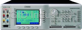
FLUKE 9100FT
Description
FLUKE=9100FT=Logic / Signature Analyzer
Part Number
9100FT
Price
Request Quote
Manufacturer
FLUKE
Lead Time
Request Quote
Category
PRODUCTS - 9
Specifications
Consumption
450VA max. 500VA max with Option 250
Depth
460mm (18.1 inches)
Height
3U
Line Frequency
48Hz to 63Hz
Power Fuses
220/240V: T3.15A HBC, 250V, IEC127
Weight
18.5kg (41lbs). 19kg (42.1lbs) with Option 250
Width
427mm (16.8 inches)
Datasheet

Extracted Text
General Specifications Line Power Supply Peak Terminal Voltages and Currents (Option 250 or 600) Voltage (single f): 100V/120V/220V/240V selectable from rear panel Peak Volts Peak to Ground Current Variation: ≤ ±10% Nominal Voltage Line Frequency: 48Hz to 63Hz SIG BNC Socket 140V 60mA TRIG BNC Socket 3V 60mA Consumption: 450VA max. 500VA max with Option 250 Power Fuses: 220/240V: T3.15A HBC, 250V, IEC127 CAUTION: Damage will result by applying a voltage >3Vpk from an external source 100/120V: T5.0A HBC, 250V, IEC127 across the inner and outer conductors. Internal trips may operate when the live SIG OUT inner and outer conductors are shorted together. Mechanical Environmental Conditions Dimensions: Height: 3U Width: 427mm (16.8 inches) Temperature: Operating: 5°C to 40°C Depth: 460mm (18.1 inches) Transit: -20°C to 60°C <100hrs Storage: 0°C to 50°C Weight: 18.5kg (41lbs). 19kg (42.1lbs) with Option 250 Warm-up Time: 20 minutes Max. Relative Humidity (non-condensing): SAFETY Operating: +5°C to +30°C: <90%, Designed to UL1244, IEC348, IEC1010-1: Pollution +30°C to +40°C: <75%, degree 2; installation category II; Protection class I. Storage: 0°C to +50°C: <95%, Altitude Peak Terminal Voltages and Currents Operating: 0 to 2000m (6,562 ft) Peak Volts Peak Non-operating: 0 to 12,000m (40,000 ft) to Ground Current Shock: MIL-T-28800, type III, class 5, style E. SHi 1500V ——— Vibration: MIL-T-28800, type III, class 5, style E. Hi 1500V 90mA Enclosure: MIL-T-28800, type III, class 5, style E. SLo 15V ——— EMC: Designed to: Lo 15V 90mA Generic Emissions: EN50081. I+ 10V 30A Generic Immunity: EN50082. I- ——— 30A FCC Rules part 15 sub-part J class B. Aux Analog Output 15V 1.5A Accuracy Tables The Meaning of 'Accuracy' when used in the Function Accuracy Tables Accuracy includes long-term stability, temperature coefficient, linearity, load and line regulation and the traceability of factory and National calibration standards. Nothing further needs to be added to determine the Test Uncertainty Ratio over the instrument under test. N.B. These specifications apply to both the Model 9100 output terminals and at the remote end of the Model 9105 lead kit unless otherwise stated. DC Voltage Accuracy Other DC Voltage Specifications Voltage Output Accuracy * Compliance Absolute +ve & -ve Polarities ±(% of Output + Floor) Current Resolution Settling Time to within 10% of accuracy: 0.08s [1] 1Year — Tcal ±5°C Load Regulation loads <1MΩ add: (200/R ) % of output LOAD 000.000 mV to 320.000 mV 0.006% + 4.16μV < 20mA 1μV Maximum Capacitance: 1000pF. 0.32001 V to 3.20000 V 0.006% + 41.6μV < 20mA 10μV 03.2001 V to 32.0000 V 0.0065% + 416μV < 20mA 100μV 032.001 V to 320.000 V 0.0065% + 4.48mV < 6mA 1mV 0320.01 V to 1050.00 V 0.006% + 19.95mV < 6mA 10mV ∗ = For loads < 1MΩ: add load regulation error. NOTES: [1] Tcal = temperature at calibration. Factory calibration temperature = 23°C. 1 AC Voltage Accuracy (Sinusoidal Waveshape) Voltage Frequency Accuracy * Current Total Absolute [2] Output Band ± (% Output + Floor) Compliance Harmonic Resolution (Hz) Distortion [1] 1 Year - Tcal ± 5°C (% of Output) 000.000 mV to 010.000 mV 10 - 3k 0.04 + 384μV 20mA 0.06 1μV 3k - 10k 0.04 + 512μV 20mA 0.10 1μV 10k - 30k 0.06 + 960μV 20mA 0.13 1μV 30k - 50k 0.09 + 1.92mV 20mA 0.20 1μV 50k - 100k 0.20 + 5.12mV 20mA 0.32 1μV 010.001 mV to 032.000 mV 10 - 3k 0.04 + 96.0μV 20mA 0.06 1μV 3k - 10k 0.04 + 128μV 20mA 0.10 1μV 10k - 30k 0.06 + 240μV 20mA 0.13 1μV 30k - 50k 0.09 + 480μV 20mA 0.20 1μV 50k - 100k 0.20 + 1.28mV 20mA 0.32 1μV 032.001 mV to 320.000 mV 10 - 3k 0.04 + 19.2μV 20mA 0.06 1μV 3k - 10k 0.04 + 25.6μV 20mA 0.10 1μV 10k - 30k 0.06 + 48.0μV 20mA 0.13 1μV 30k - 50k 0.09 + 96.0μV 20mA 0.20 1μV 50k - 100k 0.20 + 256μV 20mA 0.32 1μV 0.32001 V to 3.20000 V 10 - 3k 0.04 + 192μV 20mA 0.06 10μV 3k - 10k 0.04 + 256μV 20mA 0.10 10μV 10k - 30k 0.06 + 480μV 20mA 0.13 10μV 30k - 50k 0.09 + 960μV 20mA 0.20 10μV 50k - 100k 0.20 + 2.56mV 20mA 0.32 10μV 03.2001 V to 32.0000 V 10 - 3k 0.04 + 1.92mV 20mA 0.10 100μV 3k - 10k 0.06 + 2.56mV 20mA 0.10 100μV 10k - 30k 0.08 + 4.80mV 20mA 0.16 100μV 30k - 50k 0.15 + 9.60mV 20mA 0.20 100μV 50k - 100k 0.35 + 32.0mV 20mA 0.32 100μV 032.001 V to 105.000 V 10 - 3k 0.04 + 6.30mV 20mA 0.10 1mV 3k - 10k 0.06 + 8.40mV 20mA 0.10 1mV 10k - 30k 0.08 + 15.8mV 20mA 0.16 1mV 30k - 50k 0.15 + 31.5mV 20mA 0.20 1mV 50k - 100k 0.35 + 105mV 20mA 0.32 1mV 105.001 V to 320.000 V 40 - 100 0.05 + 19.2mV 6mA 0.50 1mV 100 - 1k 0.05 + 19.2mV 6mA 0.32 1mV 1k - 3k 0.08 + 19.2mV 6mA 0.32 1mV 3k - 10k 0.08 + 32.0mV 20mA 0.32 1mV 10k - 20k 0.12 + 48.0mV 20mA 0.32 1mV 20k - 30k 0.15 + 64.0mV 20mA 0.32 1mV 0320.01 V to 0800.00 V 40 - 100 0.05 + 63.0mV 6mA 0.50 10mV 100 - 1k 0.05 + 63.0mV 6mA 0.32 10mV 1k - 3k 0.08 + 63.0mV 6mA 0.32 10mV 3k - 10k 0.08 + 105mV 20mA 0.32 10mV 10k - 20k † 0.12 + 158mV 20mA 0.32 10mV 20k - 30k † 0.15 + 210mV 20mA 0.32 10mV 0800.01 V to 1050.00 V 40 - 100 0.05 + 126mV 6mA 0.50 10mV 100 - 1k 0.05 + 126mV 6mA 0.32 10mV 1k - 3k 0.08 + 126mV 6mA 0.32 10mV 3k - 10k 0.08 + 210mV 20mA 0.32 10mV 10k - 20k † 0.12 + 315mV 20mA 0.32 10mV ∗ = For loads < |1MΩ|: add load regulation error. † = Availability of voltage and frequency combinations is subject to the Volt-Hertz limit (see V-Hz profile). NOTES: [1] Tcal = temperature at calibration. Factory calibration temperature = 23°C. [2] Frequency Accuracy: 25ppm of output frequency. 2 AC Voltage Volt-Hertz Profile (Sine) 40Hz 10kHz 1050V 1000V 30kHz 350V Limit = 7 1.05 x 10 V-Hz 100 kHz 10Hz 105V 105V 100V 50V Output Voltage (log scale) 10V 10 40 100 1k 3k 10k 30k 100k Output Frequency (Hz) (log scale) Frequency Spans vs Frequency Resolution Absolute Span of Frequencies Resolution 1mHz 010.000 Hz to 320.000 Hz 10mHz 0.01000 kHz to 3.20000 kHz 100mHz 00.0100 kHz to 32.0000 kHz 1Hz 000.010 kHz to 100.000 kHz AC Voltage Phase (Sine) * Output Voltage Phase Span with respect to Phase Lock In = ±180° Resolution of output voltage phase increments = 0.01° TTL Signals 1V to 3V RMS Sine Input † Voltage Selected Output Phase Error Output Phase Error Output Phase Error Output Frequency with respect to with respect to with respect to f (Hz) 'Phase Lock In' 'Phase Lock Out' 'Phase Lock In' 0.30000 V to 105.000 V 10 - 40 ±0.07°±0.07°±0.70° 40 - 65 ±0.07°±0.07°±0.14° 65 - 1k ±(0.07 + 0.001 x f)°±(0.07 + 0.001 x f)°±(0.14 + 0.001 x f)° 105.001 V to 0750.00 V ♦ 45 - 65 ±0.16°±0.16°±0.23° 65 - 1k ±(0.16 + 0.0037 x f)°±(0.16 + 0.0037 x f)°±(0.23 + 0.0037 x f)° Note: An application can be employed in which the 'Slave' frequency is set to a harmonic (multiple) of the 'Master' frequency. In this case the slave frequency must not exceed 1kHz. ∗ = If two or more 9100 units are being used in a 'Master and Slave' configuration, this specification applies only when both Master and Slave are set to the same frequency. Mark/Space ratio of the input must not be less than 1:4. † = DC-coupled input. Do not AC-couple. Up to 10mV p-p noise is rejected. ♦ = Maximum load current: 2mA; maximum load capacitance: 200pF. 3 AC Voltage Accuracy (Square-Wave) Frequency Output Voltage Span Accuracy * Current Ratios and Factors based on [2] Band RMS Peak ± (% Output + Floor) Compliance Square-Wave Unit-Value Peak [1] (Hz) 1 Year — Tcal ± 5°C Peak: 1.0000 Peak to Peak: 2.0000 10 - 1k 0V - 14.08mV 0V - 14.14mV 0.12 + 450μV20mA RMS: 0.9962 10 - 1k 14.08mV - 45.08mV 14.14mV - 45.25mV 0.12 + 150μV20mA Mean: 0.9958 10 - 1k 45.08mV - 450mV 45.25mV - 452.5mV 0.12 + 40μV20mA Crest Factor: 1.0038 10 - 1k 450mV - 4.5V 452.5mV - 4.525V 0.12 + 400μV20mA Form Factor: 1.0004 10 - 1k 4.5V - 45V 4.525V - 45.25V 0.12 + 4mV 20mA 10 - 1k 45V - 147.9V 45.25V - 148.4V 0.12 + 10mV 20mA 45 - 65 147.9V - 450V 148.4V - 452.5V 0.15 + 40mV 6mA 45 - 65 450V - 500V 452.5V - 502V 0.15 + 110mV 6mA ∗ = For loads < |1MΩ|: add load regulation error. AC Voltage Accuracy (Impulse-Wave) Frequency Output Voltage Span Accuracy * Current Ratios and Factors based on [2] Band RMS Peak ± (% Output + Floor) Compliance Impulse-Wave Unit-Value Peak [1] (Hz) 1 Year — Tcal ± 5°C Peak: 1.0000 Peak to Peak: 2.0000 10 - 1k 0V - 7.43mV 0V - 14.14mV 0.30 + 1000μV20mA RMS: 0.5270 10 - 1k 7.43mV - 23.77mV 14.14mV - 45.25mV 0.30 + 500μV20mA Mean: 0.3333 10 - 1k 23.77mV - 238mV 45.25mV - 452.5mV 0.30 + 80μV20mA Crest Factor: 1.8974 10 - 1k 238mV - 2.38V 452.5mV - 4.525V 0.30 + 800μV20mA Form Factor: 1.5811 10 - 1k 2.38V - 23.8V 4.525V - 45.25V 0.30 + 8mV 20mA 10 - 1k 23.8V - 78.05V 45.25V - 148.4V 0.30 + 20mV 20mA 45 - 65 78.05V - 238V 148.4V - 452.5V 0.35 + 80mV 6mA 45 - 65 238V - 500V 452.5V - 951V 0.35 + 200mV 6mA ∗ = For loads < |1MΩ|: add load regulation error. AC Voltage Accuracy (Triangular-Wave) Frequency Output Voltage Span Accuracy * Current Ratios and Factors based on [2] Band RMS Peak ± (% Output + Floor) Compliance Triangular-Wave Unit-Value Peak [1] (Hz) 1 Year — Tcal ± 5°C Peak: 1.0000 10 - 1k 0V - 8.16mV 0V - 14.14mV 0.15 + 500μV20mA Peak to Peak: 2.0000 10 - 1k 8.16mV - 26.11mV 14.14mV - 45.25mV 0.15 + 175μV20mA RMS: 0.5774 10 - 1k 26.11mV - 261mV 45.25mV - 452.5mV 0.15 + 40μV20mA Mean: 0.5000 10 - 1k 261mV - 2.61V 452.5mV - 4.525V 0.15 + 400μV20mA Crest Factor: 1.7321 10 - 1k 2.61V - 26.1V 4.525V - 45.25V 0.15 + 4mV 20mA Form Factor: 1.1547 10 - 1k 26.1V - 85.7V 45.25V - 148.4V 0.15 + 10mV 20mA 45 - 65 85.7V - 261V 148.4V - 452.5V 0.18 + 40mV 6mA 45 - 65 261V - 500V 452.5V - 866V 0.18 + 120mV 6mA ∗ = For loads < |1MΩ|: add load regulation error. NOTES: [1] Tcal = temperature at calibration. Factory calibration temperature = 23°C. [2] Frequency Accuracy: 25ppm of output frequency. 4 AC Voltage Accuracy (Trapezoidal-Wave) Frequency Output Voltage Span Accuracy * Current Ratios and Factors based on [2] Band RMS Peak ± (% Output + Floor) Compliance Trapezoidal-Wave Unit-Value Peak [1] (Hz) 1 Year — Tcal ± 5°C Peak: 1.0000 10 - 1k 0V - 12.56mV 0V - 14.14mV 0.12 + 450μV20mA Peak: 1.0000 10 - 1k 12.56mV - 40.19mV 14.14mV - 45.25mV 0.12 + 150μV20mA Peak to Peak: 2.0000 10 - 1k 40.19mV - 402mV 45.25mV - 452.5mV 0.12 + 40μV20mA RMS: 0.8819 10 - 1k 402mV - 4.02V 452.5mV - 4.525V 0.12 + 400μV20mA Mean: 0.8333 10 - 1k 4.02V - 40.2V 4.525V - 45.25V 0.12 + 4mV 20mA Crest Factor: 1.3390 10 - 1k 40.2V - 131.9V 45.25V - 148.4V 0.12 + 10mV 20mA Form Factor: 1.0583 45 - 65 131.9V - 402V 148.4V - 452.5V 0.15 + 40mV 6mA 45 - 65 402V - 500V 452.5V - 566V 0.15 + 110mV 6mA ∗ = For loads < |1MΩ|: add load regulation error. Waveshape Harmonic Analysis (Peak values as a percentage of the Fundamental's Peak Value) (Applies also to AC Current Waveshapes) Harmonic Square Impulse Triangular Trapezoidal 1 100.00 100.00 100.00 100.00 3 -33.32 60.71 11.11 -22.22 5 19.98 14.93 4.000 4.000 7 -14.25 -7.616 2.041 2.041 9 11.07 -6.746 1.235 -2.469 11 -9.040 -0.826 0.826 0.826 13 7.626 -0.592 0.592 0.592 15 -6.590 -2.428 0.444 -0.889 17 5.795 -1.291 0.346 0.346 19 -5.165 1.034 0.277 0.277 21 4.654 1.239 0.227 -0.454 23 -4.230 0.189 0.189 0.189 25 3.872 0.160 0.160 0.160 27 -3.565 0.750 0.137 -0.274 29 3.300 0.444 0.119 0.119 31 -3.068 -0.388 0.104 0.104 33 2.862 -0.502 0.092 -0.184 35 -2.679 -0.082 0.082 0.082 37 2.515 -0.073 0.073 0.073 39 -2.368 -0.359 0.066 -0.131 41 2.230 -0.222 0.060 0.060 Other AC Voltage Specifications Settling Time (to within 10% of accuracy): ≤105V: 0.08s; >105V: 0.5s. Load Regulation: 2 For loads <|1MΩ| ≤105V, add: [(200/R ) + (C * x F x 0.03)] % of output LOAD LOAD 2 For loads <|1MΩ| >105V, add: [(200/R ) + (C * x F x 0.19 + C * • 3E7)] % of output LOAD LOAD LOAD * = To calculate C limit from Current compliance specification, while using 9105 lead set, allow ≈ 30pF for lead set. LOAD Maximum Capacitance: 1000pF; subject to Output Current Limitations at HF. 5 DC Current Accuracy Equivalent Accuracy Compliance Compliance Absolute Current Output ±(% of Output + Floor) Voltage Voltage Resolution [1] +ve & -ve Polarities 1Year — Tcal ±5°C (at 9100 terminals) (at 9105 lead end) 000.000μA - 320.000μA 0.014 + 11nA 4V 4V 1nA 0.32001mA - 3.20000mA 0.014 + 83nA 4V 4V 10nA 03.2001mA - 32.0000mA 0.014 + 900nA 4V 4V 100nA 032..001mA - 320.000mA 0.016 + 9.6μA4V 4V 1μA 0.32001A - 3.20000A 0.060 + 118μA 2.2V 2.2V 10μA 03.2001A - 10.5000A 0.055 + 940μA 2.2V 2.1V 100μA 10.5001A - 20.0000A * 0.055 + 4.50mA 2.2V 2.0V 100μA ∗ = With output 'ON', maximum duty cycle of (>0.525FS : ≤0.525FS) is (1 : 4). Continuous output >0.525FS will automatically reduce to <0.525FS after 2 Minutes. Option 200 — DC Current Accuracy via Current Coils Equivalent Accuracy † Absolute Current Output ±(% of Output + Floor) Resolution [1] +ve & -ve Polarities 1Year — Tcal ±5°C 10-Turn Coil: 03.2001A - 32.0000 A 0.060 + 1.18mA 100μA 032.001A - 105.000A 0.055 + 9.40mA 1mA 105.001A - 200.000 A * 0.055 + 45.0mA 1mA 50-Turn Coil: 016.001A - 160.000A 0.060 + 5.9mA 1mA 0160.01A - 0525.00A 0.055 + 47mA 10mA 0525.01A - 1000.00 A * 0.055 + 225mA 10mA ∗ = With output 'ON', maximum duty cycle of (>0.525FS : ≤0.525FS) is (1 : 4). Continuous output >0.525FS will automatically reduce to <0.525FS after 2 Minutes. † = Refers to accuracy at 9100 output terminals. With Option 200 coils connected, then at the output from the coils, add ±0.2% of output from coils for uncertainty of coils. Other DC Current Specifications Settling Time to within 10% of accuracy: 0.08s Maximum Terminal Inductance: 0 - 3.2mA : 50μH 3.2mA - 320mA : 30μH 320mA - 3.2A : 18μH 3.2A - 10.5A : 5.5μH 10.5A - 20A : 2.5μH (With 10 turn or 50 turn output selected): 3.2A - 1000A : 700μH NOTES: [1] Tcal = temperature at calibration. Factory calibration temperature = 23°C. 6 AC Current Accuracy (Sinusoidal Waveshape) Compliance Absolute Current Frequency Accuracy † Compliance Compliance Total Compliance Absolute Voltage Resolution [2] Output Band Voltage Voltage Harmonic Error (A/V) Resolution at 9105 lead end) (Hz) ± (% Output + Floor) (VRMS at 9100 (VRMS at 9105 Distortion for 4V 1nA [1] 1 Year - Tcal ± 5°C terminals) Lead End) (% Output) Vc>0.5VRMS 4V 10nA 4V 100nA 000.000μA - 032.000μA 10 - 3k 0.07 + 900nA 4V 4V 0.10 60nA/V 1nA 4V 1μA 3k - 10k 0.10 + 1.8μA 4V 4V 0.25 600nA/V 1nA 10k - 20k 0.20 + 6.0μA 4V 4V 0.40 2.4μA/V 1nA 2.2V 10μA 20k - 30k 0.25 + 9.0μA 4V 4V 0.60 5.4μA/V 1nA 2.1V 100μA 032.001μA - 320.000μA 10 - 3k 0.07 + 300nA 4V 4V 0.10 60nA/V 1nA 2.0V 100μA 3k - 10k 0.10 + 600nA 4V 4V 0.25 600nA/V 1nA 10k - 20k 0.20 + 2.0μA 4V 4V 0.40 2.4μA/V 1nA 20k - 30k 0.25 + 3.0μA 4V 4V 0.60 5.4μA/V 1nA 0.32001mA - 3.20000mA 10 - 3k 0.07 + 300nA 4V 4V 0.10 60nA/V 10nA 3k - 10k 0.10 + 600nA 4V 4V 0.25 600nA/V 10nA 10k - 20k 0.20 + 2.0μA 4V 4V 0.40 2.4μA/V 10nA 20k - 30k 0.25 + 3.0μA 4V 4V 0.60 5.4μA/V 10nA 03.2001mA - 32.0000mA 10 - 3k 0.07 + 3.2μA 4V 4V 0.10 0.5μA/V 100nA 3k - 10k 0.10 + 6.4μA 4V 4V 0.25 4μA/V 100nA 10k - 20k 0.20 + 12.8μA 4V 4V 0.40 15μA/V 100nA 20k - 30k 0.25 + 22.4μA 4V 4V 0.60 32μA/V 100nA 032.001mA - 320.000mA 10 - 3k 0.08 + 32.0μA 4V 4V 0.10 2μA/V 1μA 3k - 10k 0.10 + 48.0μA 4V 4V 0.25 4μA/V 1μA 10k - 20k 0.20 + 64.0μA 4V 4V 0.40 15μA/V 1μA 20k - 30k 0.25 + 96.0μA 4V 4V 0.60 35μA/V 1μA 0.32001A - 3.20000A 10 - 3k 0.10 + 480μA 2.5V 2.4V 0.20 90μA/V 10μA 3k - 10k 0.25 + 2.56mA 2.5V 2.4V 1.10 600μA/V 10μA 03.2001A - 10.5000A 10 - 3k 0.20 + 3.0mA 2.5V 2.3V 0.20 0.3mA/V 100μA 3k - 10k 0.50 + 10.0mA 2.2V 2.0V 1.10 2.1mA/V 100μA 10.5001A - 20.0000A ♠ 10 - 3k 0.20 + 6.9mA 2.5V ♦ 2.2V ♦ 0.30 0.3mA/V 100μA 3k - 10k 0.50 + 23.0mA 2.1V 1.7V 1.50 2.1mA/V 100μA 03.2001A - 32.0000A ♥ 10 - 100 0.20 + 5.5mA 2.5V 2.5V 0.15 --- 100μA 100 - 440 0.78 + 27mA 2.5V 2.5V 0.50 --- 100μA 032.001A - 200.000A♠♥ 10 - 100 0.21 + 90mA 2.5V ♦ 2.3V ♦ 0.15 --- 1mA 100 - 440 0.67 + 0.25A 2.5V 2.3V 0.50 --- 1mA 016.001A - 160.000A ♣ 10 - 100 0.20 + 28mA 2.5V 2.5V 0.15 --- 1mA 0160.01A - 1000.00A♠♣ 10 - 100§ 0.21 + 0.45A 2.5V ♦ 2.3V ♦ 0.15 --- 10mA † = Total uncertainty includes compliance errors for Voltage ≤0.5VRMS. Above 0.5V, add appropriate compliance error, except for Outputs marked ♥ and ♣. ♠ = With output 'ON', maximum duty cycle of (>0.525FS : ≤0.525FS) is (1 : 4). Continuous output >0.525FS will automatically reduce to <0.525FS after 2 Minutes. ♥ = Accuracy at 9100 output terminals, option 200 10 turn coil connected. For the output from the coil, add ±0.2% of output from coil for uncertainty of coil. ♣ = Accuracy at 9100 output terminals, option 200 50 turn coil connected. For the output from the coil, add ±0.2% of output from coil for uncertainty of coil. ♦ = For frequencies <40Hz, compliance voltage is reduced by 0.5V RMS. § = These coils have been designed for optimum accuracy and inductance for use with the Model 9100. With some clamp meters, especially those using Hall effect, the increase in inductance due to the current clamp design will limit the obtainable 9100 Current/Hertz profile. In some cases, 1000A cannot be reached at higher frequency. Frequency Spans vs Frequency Resolutions Absolute Span of Frequencies Resolution 1mHz 010.000 Hz to 320.000 Hz 10mHz 0.01000 kHz to 3.20000 kHz 100mHz 00.0100 kHz to 30.0000 kHz NOTES: [1] Tcal = temperature at calibration. Factory calibration temperature = 23°C. [2] Frequency Accuracy: 25ppm of output frequency. 7 AAAAAAAAAAAAAAAAAAAAAAAAAAAAAAAAAAA AC Current Amp-Hertz Profile (Sine) 10Hz 65Hz 1000A 1000A 440Hz 200A 200A 100A 9100 + Option 200 10kHz 20A 20A 10A 1A 30kHz 320mA 320mA 9100 No Option 200 100mA 10mA Output Current (log scale) 10 100 1k 10k 20k 30k Output Frequency (Hz) (log scale) AC Current Phase (Sine) * Output Current Phase Span with respect to Phase Lock In = ±180° Resolution of output voltage phase increments = 0.01° TTL Signals 1V to 3V RMS Sine Input † Current Selected Output Phase Error Output Phase Error Output Phase Error Output Frequency with respect to with respect to with respect to f (Hz) 'Phase Lock In' 'Phase Lock Out' 'Phase Lock In' 0.00000 A - 20.0000 A 10 - 40 ±0.08°±0.08°±0.71° 40 - 65 ±0.08°±0.08°±0.15° 65 - 1k ±(0.08 + 0.0008 x f)°±(0.08 + 0.0008 x f)°±(0.15 + 0.001 x f)° 03.2000 A - 1000.00 A ♠ 10 - 40 ±0.23°±0.23°±0.8° 40 - 65 ±0.23°±0.23°±0.3° 65 - 1k ±(0.23 + 0.003 x f)°±(0.23 + 0.003 x f)°±(0.3 + 0.0037 x f)° Note: An application can be employed in which the 'Slave' frequency is set to a harmonic (multiple) of the 'Master' frequency. In this case the slave frequency must not exceed 1kHz. ∗ = If two or more 9100 units are being used in a 'Master and Slave' configuration, this specification applies only when both Master and Slave are set to the same frequency. Mark/Space ratio of the input must not be less than 1:4. † = DC-coupled input. Do not AC-couple. Up to 10mV p-p noise is rejected. ♠ = With 10-turn or 50-turn output selected (Option 200). Other AC Current Specifications Settling Time to within 10% of accuracy: 0.08s Maximum Terminal Inductance: 0 - 3.2mA : 50μH 3.2mA - 320mA : 30μH 320mA - 3.2A : 18μH 3.2A - 10.5A : 5.5μH 10.5A - 20A : 2.5μH (With 10 turn or 50 turn output selected): 3.2A - 1000A : 700μH 8 AC Current Accuracy (Square-Wave) Frequency Output Current Span Accuracy † Voltage Ratios and Factors based on [2] Band RMS Peak ± (% Output + Floor) Compliance Square-Wave Unit-Value Peak [1] (Hz) 1 Year — Tcal ± 5°C (VRMS) Peak: 1.0000 Peak to Peak: 2.0000 10 - 1k 0μA - 45.08μA 0V - 45.25μA 0.21 + 1.8μA 4.0 RMS: 0.9962 10 - 1k 45.08μA - 4.508mA 45.25μA - 4.525mA 0.21 + 0.6μA 4.0 Mean: 0.9958 10 - 1k 4.508mA - 45.08mA 4.525mA - 45.25mA 0.21 + 6.4μA 4.0 Crest Factor: 1.0038 10 - 1k 45.08mA - 450.8mA 45.25mA - 452.5mA 0.24 + 64μA 4.0 Form Factor: 1.0004 10 - 100 0.4508A - 3.200A 0.4525A - 3.212A 0.30 + 960μA 2.2 10 - 100 3.200A - 18.00A* 3.212A - 18.07A 0.4 + 13.8mA 2.2 ♦ 10 - 65 4.508A - 32.00A ♥ 4.525A - 32.12A 1.0 + 16.8mA 2.2 10 - 65 32.00A - 180.0A*♥ 32.12A - 180.7A 1.2 + 162mA 2.2 ♦ 10 - 65 22.54A - 160.0A ♣ 22.63A - 160.6A 1.0 + 84mA 2.2 10 - 65 160.0A - 900.0A*♣ 160.6A - 903.5A 1.2 + 0.82A 2.2 ♦ ∗ = With output 'ON', maximum duty cycle of (>0.528FS : ≤0.528FS) is (1 : 4). Continuous output >0.528FS will automatically reduce to <0.528FS after 2 Minutes. † = Total uncertainty includes compliance errors for Voltage ≤0.5VRMS. Above 0.5V, add appropriate compliance error, except for Outputs marked ♥ and ♣. ♥ = Refers to accuracy at 9100 output terminals. With Option 200 10 turn coil connected, then at the output from the coil, add ±0.2% of output from coil for uncertainty of coil. ♣ = Refers to accuracy at 9100 output terminals. With Option 200 50 turn coil connected, then at the output from the coil, add ±0.2% of output from coil for uncertainty of coil. ♦ = For frequencies <40Hz, compliance voltage is reduced by 0.5V RMS. AC Current Accuracy (Impulse-Wave) Frequency Output Current Span Accuracy † Voltage Ratios and Factors based on [2] Band RMS Peak ± (% Output + Floor) Compliance Impulse-Wave Unit-Value Peak [1] (Hz) 1 Year — Tcal ± 5°C (VRMS) Peak: 1.0000 10 - 1k 0μA - 23.79μA 0V - 45.25μA 0.42 + 2.7μA 3.0 Peak to Peak: 2.0000 10 - 1k 23.79μA - 2.379mA 45.25μA - 4.525mA 0.42 + 0.9μA 3.0 RMS: 0.5270 10 - 1k 2.379mA - 23.79mA 4.525mA - 45.25mA 0.42 + 9.6μA 3.0 Mean: 0.3333 10 - 1k 23.79mA - 237.9mA 45.25mA - 452.5mA 0.48 + 96μA 3.0 Crest Factor: 1.8974 10 - 100 0.2379A - 2.379A 0.4525A - 4.525A 0.60 + 1.44mA 1.8 Form Factor: 1.5811 10 - 100 2.379A - 15.00A* 4.525A - 28.53A 0.80 + 20.7mA 1.8 ♦ 10 - 65 2.379A - 23.79A ♥ 4.525A - 45.25A 0.80 + 25.2mA 1.8 10 - 65 23.79A - 150.0A*♥ 45.25A - 285.3A 1.20 + 243mA 1.8 ♦ 10 - 65 11.90A - 118.9A ♣ 22.63A - 226.3A 0.80 + 126mA 1.8 10 - 65 118.9A - 750.0A*♣ 226.3A - 1426A 1.20 + 1.23A 1.8 ♦ ∗ = With output 'ON', maximum duty cycle of (>0.7FS : ≤0.7FS) is (1 : 4). Continuous output >0.525FS will automatically reduce to <0.525FS after 2 Minutes. † = Total uncertainty includes compliance errors for Voltage ≤0.5VRMS. Above 0.5V, add appropriate compliance error, except for Outputs marked ♥ and ♣. ♥ = Refers to accuracy at 9100 output terminals. With Option 200 10 turn coil connected, then at the output from the coil, add ±0.2% of output from coil for uncertainty of coil. ♣ = Refers to accuracy at 9100 output terminals. With Option 200 50 turn coil connected, then at the output from the coil, add ±0.2% of output from coil for uncertainty of coil. ♦ = For frequencies <40Hz, compliance voltage is reduced by 0.5V RMS. NOTES: [1] Tcal = temperature at calibration. Factory calibration temperature = 23°C. [2] Frequency Accuracy: 25ppm of output frequency. 9 AC Current Accuracy (Triangular-Wave) Frequency Output Current Span Accuracy † Voltage Ratios and Factors based on [2] Band RMS Peak ± (% Output + Floor) Compliance Triangular-Wave Unit-Value Peak [1] (Hz) 1 Year — Tcal ± 5°C (VRMS) Peak: 1.0000 Peak to Peak: 2.0000 10 - 1k 0μA - 26.12μA0μA - 45.25μA 0.21 + 1.8μA 3.2 10 - 1k 26.12μA - 2.612mA 45.25μA - 4.525mA 0.21 + 0.6μA 3.2 RMS: 0..5774 Mean: 0.5000 10 - 1k 2.612mA - 26.12mA 4.525mA - 45.25mA 0.21 + 6.4μA 3.2 Crest Factor: 1.7321 10 - 1k 26.12mA - 261.2mA 45.25mA - 452.5mA 0.24 + 64μA 3.2 Form Factor: 1.1547 10 - 100 0.2612A - 2.612A 0.4525A - 4.525A 0.30 + 960μA 2.0 10 - 100 2.612A - 16.30A* 4.525A - 28.23A 0.40 + 13.8mA 2.0 ♦ 10 - 65 2.612A - 26.12A ♥ 4.525A - 45.25A 0.40 + 16.8mA 2.0 10 - 65 26.12A - 163.0A*♥ 45.25A - 282.3A 0.60 + 162mA 2.0 ♦ 10 - 65 13.06A - 130.6A ♣ 22.62A - 226.2A 0.40 + 84mA 2.0 10 - 65 130.6A - 815.0A*♣ 226.2A - 1411A 0.60 + 0.82A 2.0 ♦ ∗ = With output 'ON', maximum duty cycle of (>0.644FS : ≤0.644FS) is (1 : 4). Continuous output >0.644FS will automatically reduce to <0.644FS after 2 Minutes. † = Total uncertainty includes compliance errors for Voltage ≤0.5VRMS. Above 0.5V, add appropriate compliance error, except for Outputs marked ♥ and ♣. ♥ = Refers to accuracy at 9100 output terminals. With Option 200 10 turn coil connected, then at the output from the coil, add ±0.2% of output from coil for uncertainty of coil. ♣ = Refers to accuracy at 9100 output terminals. With Option 200 50 turn coil connected, then at the output from the coil, add ±0.2% of output from coil for uncertainty of coil. ♦ = For frequencies <40Hz, compliance voltage is reduced by 0.5V RMS. AC Current Accuracy (Trapezoidal-Wave) Ratios and Factors based on Frequency Output Current Span Accuracy † Voltage Trapezoidal-Wave Unit-Value Peak [2] Band RMS Peak ± (% Output + Floor) Compliance [1] (Hz) 1 Year — Tcal ± 5°C (VRMS) Peak: 1.0000 Peak to Peak: 2.0000 10 - 1k 0μA - 39.91μA 0V - 45.25μA 0.21 + 1.8μA 4.0 RMS: 0.8819 10 - 1k 39.91μA - 3.991mA 45.25μA - 4.525mA 0.21 + 0.6μA 4.0 Mean: 0.8333 10 - 1k 3.991mA - 39.91mA 4.525mA - 45.25mA 0.21 + 6.4μA 4.0 Crest Factor: 1.3389 10 - 1k 39.91mA - 399.1mA 45.25mA - 452.5mA 0.24 + 64μA 4.0 Form Factor: 1.0583 10 - 100 0.3991A - 3.200A 0.4525A - 3.628A 0.30 + 960μA 2.3 10 - 100 3.200A - 19.20A* 3.628A - 21.77A 0.40 + 13.8mA 2.3 ♦ 10 - 65 3.991A - 32.00A ♥ 4.525A - 36.28A 0.40 + 16.8mA 2.3 10 - 65 32.00A - 192.0A*♥ 36.28A - 217.7A 0.60 + 162mA 2.3 ♦ 10 - 65 19.95A - 160.0A ♣ 22.62A - 181.4A 0.40 + 84mA 2.3 10 - 65 160.0A - 960.0A*♣ 181.4A - 1088A 0.60 + 0.82A 2.3 ♦ ∗ = With output 'ON', maximum duty cycle of (>0.547FS : ≤0.547FS) is (1 : 4). Continuous output >0.547FS will automatically reduce to <0.547FS after 2 Minutes. † = Total uncertainty includes compliance errors for Voltage ≤0.5VRMS. Above 0.5V, add appropriate compliance error, except for Outputs marked ♥ and ♣. ♥ = Refers to accuracy at 9100 output terminals. With Option 200 10 turn coil connected, then at the output from the coil, add ±0.2% of output from coil for uncertainty of coil. ♣ = Refers to accuracy at 9100 output terminals. With Option 200 50 turn coil connected, then at the output from the coil, add ±0.2% of output from coil for uncertainty of coil. ♦ = For frequencies <40Hz, compliance voltage is reduced by 0.5V RMS. Waveshape Harmonic Analysis (Refer to AC Voltage Waveshapes) NOTES: [1] Tcal = temperature at calibration. Factory calibration temperature = 23°C. [2] Frequency Accuracy: 25ppm of output frequency. 10 Resistance Accuracy Resistance Output Accuracy Absolute Resolution (Source UUTi Low) (Source UUTi High) (Source UUTi Super) ±(% of Output + Floor) ±(% of Output + Floor) ±(% of Output + Floor) [1] [1] [1] 1Year - Tcal ±5°C 1Year - Tcal ±5°C 1Year - Tcal ±5°C 00.0000 Ω to 40.0000 Ω 0.025 + 10.0mΩ 0.050 + 20.0mΩ 0.100 + 50.0mΩ 0.1mΩ 040.001 Ω to 400.000 Ω 0.020 + 20.0mΩ ∗ 0.015 + 20.0mΩ 0.035 + 100mΩ 1mΩ 0.40001 kΩ to 4.00000 kΩ 0.015 + 80.0mΩ 0.015 + 80.0mΩ 0.035 + 200mΩ 10mΩ 04.0001 kΩ to 40.0000 kΩ 0.020 + 800mΩ 0.015 + 800mΩ 0.025 + 2.0Ω 100mΩ 040.001 kΩ to 400.000 kΩ 0.020 + 8.0Ω 0.018 + 8.0Ω 0.025 + 20Ω 1Ω 0.40001 MΩ to 4.00000 MΩ 0.050 + 100Ω 0.020 + 100Ω 0.040 + 200Ω 10Ω 04.0001 MΩ to 40.0000 MΩ 0.150 + 2.0kΩ 0.050 + 2.0kΩ 0.050 + 2.0kΩ 100Ω 040.001 MΩ to 400.000 MΩ 0.260 + 40.0kΩ 0.060 + 40.0kΩ --- 1kΩ ∗ = Valid for UUTi ≥ 200μA. Below 200μA: new floor = (200μA ÷ Actual UUTi) x 20mΩ. Source Current Limits Hardware Configuration Limits Source Current Limits on Span of Output Resistance UUTi Low UUTi High UUTi Super 00.0000 Ω to 40.0000 Ω 250μA to 3.5mA 2.5mA to 35mA 25mA to 350mA 040.001 Ω to 400.000 Ω 25μA to 320μA 250μA to 3.5mA 2.5mA to 35mA 0.40001 kΩ to 4.00000 kΩ 25μA to 320μA 250μA to 3.5mA 2.5mA to 35mA 04.0001 kΩ to 40.0000 kΩ 2.5μAto 32μA25μA to 350μA 250μA to 3.5mA 040.001 kΩ to 400.000 kΩ 250nA to 3.2μA 2.5μAto 35μA25μA to 350μA 0.40001 MΩ to 4.00000 MΩ 25nA to 320nA 250nA to 3.5μA 2.5μAto 35μA 04.0001 MΩ to 40.0000 MΩ 8nA to 32nA 25nA to 350nA 250nA to 3.5μA 040.001 MΩ to 400.000 MΩ 4nA to 32nA 25nA to 200nA N/A Other Resistance Specifications Maximum Measurement Voltage: 10V; (I x R = ≤10V) measure actual Settling Time to within 10% of accuracy: 0 - 40kΩ : <0.08s 40kΩ -4MΩ : <0.3s 4MΩ -400MΩ : <1s 4-wire Lead Compensation: Max total lead resistance: 50Ω Nominal lead resistance rejection: 10000:1 NOTES: [1] Tcal = temperature at calibration. Factory calibration temperature = 23°C. 11 Ω Conductance Accuracy Conductance Span vs Resolution Conductance Output Accuracy ±(% Output) [1] 1Year — Tcal ±5°C Absolute Span of Values UUTi Low & High UUTi Super Resolution 2.5nS - 25.0nS 0.40 N/A 0.1pS 02.5000 nS to 25.0000 nS 25.0nS - 250.0nS 0.20 0.45 1pS 002.500 nS to 250.000 nS 250.0nS - 2.5μS 0.12 0.27 10pS 0.00250 μS to 2.50000 μS 2.5μS - 25.0μS 0.05 0.12 100pS 00.0025 μS to 25.0000 μS 25.0μS - 250.0μS 0.05 0.12 1nS 000.002 μS to 250.000 μS 250.0μS - 2.5mS 0.04 0.09 10nS 0.00001 mS to 2.50000 mS Source Current Limits Hardware Configuration Limits Current Source Limits on Span of Output Conductance UUTi Low UUTi High UUTi Super 02.5000 nS to 25.0000 nS 4nA to 32nA 2.5nA to 200nA N/A 025.001 nS to 250.000 nS 8nA to 32nA 25nA to 350nA 250nA to 3.5μA 0.25001 μS to 2.50000 μS 25nA to 320nA 250nA to 3.5μA 2.5μAto35μA 02.5001 μS to 25.0000 μS 250nA to 3.2μA 2.5μAto 35μA25μA to 350μA 025.001 μS to 250.000 μS 2.5μAto32μA25μA to 350μA 250μA to 3.5mA 0.25001 mS to 2.50000 mS 25μA to 320μA 250μA to 3.5mA 2.5A to 35mA Other Conductance Specifications Maximum Measurement Voltage: 10V; (I ÷ = ≤10V) measure actual Settling Time to within 10% of accuracy: 2.5nS - 250nS : <1s 250nS - 25μS : <0.3s 25μS - 2.5mS : <0.08s 4-wire Lead Compensation: Max total lead resistance: 50Ω Nominal lead resistance rejection: 10000:1 NOTES: [1] Tcal = temperature at calibration. Factory calibration temperature = 23°C. 12 Frequency Function Accuracy Frequency Output Accuracy Accuracy Mark/Period Ratio ±(ppm of Output Frequency) ±(ppm of Output Frequency) (%) [1] [1] 1Year — Tcal ±5°C 5Year — Tcal ±5°C Standard Option 100 0.5Hz - 10.0MHz 25.0 0.25 50 High and Low Voltage Limits and Voltage Accuracy Frequency Output Accuracy Span Voltage Vo (±Volts) [1] 1Year — Tcal ±5°C 0.5Hz to 2MHz Vo ≤ 6Vpk 0.06V † 2MHz to 10MHz Vo ≤ 6Vpk 1.0V 0.5Hz to 1kHz 6Vpk < Vo ≤ 30Vpk 0.3V † = After first 150ns. Frequency Spans vs Frequency Resolution Absolute Span of Frequencies Output Voltage Resolution ≤6Vpk >6Vpk 1mHz 000.500 Hz to 320.000 Hz ∗∗ 10mHz 0.00050 kHz to 1.00000 kHz ∗∗ 10mHz 1.00001 kHz to 3.20000 kHz ∗ --- 100mHz 00.0005 kHz to 32.0000 kHz ∗ --- 1Hz 000.001 kHz to 320.000 kHz ∗ --- 10Hz 0.00001 MHz to 3.20000 MHz ∗ --- 100Hz 00.0001 MHz to 10.0000 MHz ∗ --- * = Peak outputs available at stated levels. Rise Times (Specified into loads R > 100kΩ in parallel with C ≤ 100pF) L L For signals ≤ 6Vpk : <40ns. For signals > 6Vpk : <1.5μs. High Level = +5V Mark Space Low Level = 500µs = 500µs = 0V Period = 1ms Repetition Rate = 1kHz Frequency Function — Default Output Waveshape NOTES: [1] Tcal = temperature at calibration. Factory calibration temperature = 23°C. 13 Mark/Period Function — Pulse Width and Repetition Period Intervals Accuracy Output Interval Accuracy Option 100 Accuracy Voltage ±(ppm of Output + Floor) ±(ppm of Output + Floor) [1] [1] 1Year — Tcal ±5°C 5Year — Tcal ±5°C Vo ≤ 6Vpk Pulse Width: 0.30μs to 1999.99ms 25 + 10ns 0.25 + 10ns Repetition Period: 0.6μs to 2000ms 25 0.25 6Vpk < Vo ≤ 30Vpk Pulse Width: 10μs to 1999.99ms 25 + 200ns 0.25 + 200ns Repetition Period: 1ms to 2000ms 25 0.25 High and Low Voltage Limits and Voltage Accuracy Output Accuracy Voltage Vo (±Volts) [1] 1Year — Tcal ±5°C Vo ≤ 6Vpk 0.06V † 6Vpk < Vo ≤ 30Vpk 0.3V † = After first 150ns. Repetition Period Interval Pulse Width Interval Spans vs Time Resolution Spans vs Time Resolution Absolute ≤6V pk >6Vpk Absolute ≤6V pk >6Vpk Resolution Resolution 100ns 000.6 μs to 999.9 μs ----- 100ns 000.3 μs to 999.9 μs* 010.00 μs to 990.0 μs** 100ns 00.0006 ms to 99.9999 ms 01.0000 ms to 99.9999 ms 100ns 00.0003 ms to 99.9999 ms* 00.0100 ms to 99.9999 ms** 1μs 000.001 ms to 999.999 ms 001.000 ms to 999.999 ms 1μs 000.001 ms to 999.999 ms 000.010 ms to 999.999 ms** 10μs 0000.01 ms to 2000.00 ms 0001.00 ms to 2000.00 ms 10μs 0000.01 ms to 1999.99 ms 0000.01 ms to 1999.99 ms * = Max Pulse Width must be at least 0.3μs less than the Repetition Period. ** = Max Pulse Width must be at least 10μs less than the Repetition Period. Rise Times (Specified into loads R > 100kΩ in parallel with C ≤ 100pF) L L For signals ≤ 6Vpk : <40ns. For signals > 6Vpk : <1.5μs. Pulse Width ('Mark') High Level 'Space' Low Level Repetition Period Repetition Rate = 1/Repetition Period Mark/Period Function — Generalized Output Waveshape Definition NOTES: [1] Tcal = temperature at calibration. Factory calibration temperature = 23°C. 14 '% Duty' Function — '% Duty' Value: Repetition Period Intervals Accuracy Screen Setting Limits Output Interval Accuracy Option 100 Accuracy 00.05% ≤ % Duty ≤ 99.95% Voltage ±(ppm of Output) ±(ppm of Output) [1] [1] 1Year — Tcal ±5°C 5Year — Tcal ±5°C Vo ≤ 6Vpk 100μs to 2000ms 25 0.25 6Vpk < Vo ≤ 30Vpk 1ms to 2000ms 25 0.25 Duty Cycle Accuracy High and Low Voltage Limits and Voltage Accuracy Output Voltage Total Accuracy [1] 1Year — Tcal ±5°C Output Accuracy Voltage Vo (±Volts) Vo ≤ 6Vpk 35ns [1] 1Year — Tcal ±5°C 6Vpk < Vo ≤ 30Vpk ‡ 225ns Vo ≤ 6Vpk 0.06V † ‡ = Minimum Mark or Space interval: 10μs. 6Vpk < Vo ≤ 30Vpk 0.3V † = After first 150ns. Rise Times Repetition Period Interval Spans vs Time Resolution (Specified into loads R > 100kΩ in parallel with C ≤ 100pF) L L For signals ≤ 6Vpk : <40ns. Absolute ≤6V pk >6Vpk Resolution For signals > 6Vpk : <1.5μs. 100ns 100.0 μs to 999.9 μs ----- 100ns 00.1000 ms to 99.9999 ms 01.0000 ms to 99.9999 ms 1μs 000.001 ms to 999.999 ms 001.000 ms to 999.999 ms 10μs 0000.01 ms to 2000.00 ms 0001.00 ms to 2000.00 ms Pulse Width ('Mark') High Level 'Space' Low Level Repetition Period Repetition Rate = 1/Repetition Period Pulse Width % Duty Cycle = X 100% Repetition Period % Duty Cycle Function — Generalized Output Waveshape Definition NOTES: [1] Tcal = temperature at calibration. Factory calibration temperature = 23°C. 15 Capacitance Accuracy Capacitance Output Accuracy * Absolute Resolution Source UUTi Low Source UUTi Super [1] [1] ±(% of Output + Floor) 1Year — Tcal ±5°C ±(% of Output + Floor) 1Year — Tcal ±5°C Stim Repetition Rate Stim Repetition Rate Stim Repetition Rate Stim Repetition Rate ≤ 350Hz 350Hz to 1.5kHz ≤ 350Hz 350Hz to 1.5kHz 0.5000 nF to 4.0000 nF 0.3 + 15pF 0.6 +30.0pF ----- ----- 0.1pF 4.0001 nF to 40.000 nF 0.3 + 30pF 0.6 +60.0pF ----- ----- 1pF 40.001 nF to 400.00 nF 0.3 + 160pF 0.6 +320pF ----- ----- 10pF 400.01 nF to 4.0000 μF 0.4 + 1.6nF 0.8 +3.2nF ----- ----- 100pF 4.0001 μF to 40.000 μF 0.5 + 16.0nF 1.0 +32.0nF ----- ----- 1nF 40.001 μF to 400.00 μF 0.5 + 160nF 1.0 +320nF 0.75 + 160nF 1.0 + 320nF 10nF 400.01 μF to 4.0000 mF 0.5 + 1.6μF 1.0 +3.2μF 0.75 + 1.6μF 1.0 + 3.2μF 100nF 4.0001 mF to 40.000 mF 1.0 + 60μF 2.0 +120μF 1.0 + 60μF 2.0 + 120μF1μF * = Accuracy specifications apply both at the 9100 output terminals, and at the output leads of the Model 9105 leadset. Measurement and Discharge Current Capacitance Output Source UUTi Low Source UUTi Super Measurement Maximum Measurement Maximum Current Range Discharge Current Current Range Discharge Current 0.5000 nF to 4.0000 nF 0.02μA to 500μA 1mA ----- ----- 4.0001 nF to 40.000 nF 0.02μA to 500μA 5mA ----- ----- 40.001 nF to 400.00 nF 0.04μA to 1mA 10mA ----- ----- 400.01 nF to 4.0000 μF 0.5μA to 1mA 10mA ----- ----- 4.0001 μF to 40.000 μF5μA to 3mA 10mA ----- ----- 40.001 μF to 400.00 μF5μA to 3mA 10mA 50μA to 30mA 100mA 400.01 μF to 4.0000 mF 5μA to 3mA 10mA 50μA to 30mA 100mA 4.0001 mF to 40.000 mF 5μA to 3mA 10mA 50μA to 30mA 100mA Other Capacitance Specifications Maximum Measurement Voltage: ±3.5V (except 40μF range which is limited to ±2.5V) Settling Time to within 10% of accuracy: <0.08s 4-wire Lead Compensation: Max total lead resistance: 10Ω NOTES: [1] Tcal = temperature at calibration. Factory calibration temperature = 23°C. 16 Thermocouple Other Thermocouple Temperature Accuracy Output Specifications Settling Time to within 10% of accuracy: 0.08s Thermocouple Temperature Output Accuracy * † ‡ Type (Screen Resolution (±°C) Load Regulation: (200/R ) % of output LOAD [1] Shown) 1Year — Tcal ±5°C Maximum Capacitance: 1000pF. B +0500.0°C - +0800.0°C 0.55 +0800.0°C - +1000.0°C 0.41 +1000.0°C - +1400.0°C 0.34 +1400.0°C - +1820.0°C 0.37 C 0000.0°C - +0600.0°C 0.29 +0600.0°C - +1000.0°C 0.27 +1000.0°C - +1800.0°C 0.40 +1800.0°C - +2320.0°C 0.41 E -0250.0°C - -0200.0°C 0.45 -0200.0°C - -0100.0°C 0.22 -0100.0°C - +0100.0°C 0.17 +0100.0°C - +1000.0°C 0.21 J -0210.0°C - -0100.0°C 0.25 -0100.0°C - +0800.0°C 0.19 +0800.0°C - +1000.0°C 0.21 +1000.0°C - +1200.0°C 0.23 K -0250.0°C - -0200.0°C 0.57 -0200.0°C - -0100.0°C 0.27 -0100.0°C - +0100.0°C 0.19 +0100.0°C - +0600.0°C 0.23 +0600.0°C - +1372.0°C 0.27 L -0200.0°C - -0050.0°C 0.26 -0050.0°C - +0200.0°C 0.18 +0200.0°C - +0700.0°C 0.20 +0700.0°C - +0900.0°C 0.23 N -0200.0°C - -0100.0°C 0.33 -0100.0°C - +0900.0°C 0.23 +0900.0°C - +1100.0°C 0.22 +1100.0°C - +1300.0°C 0.24 R ♦ 0000.0°C - +0100.0°C 0.52 +0100.0°C - +0200.0°C 0.40 +0200.0°C - +1600.0°C 0.35 +1600.0°C - +1767.0°C 0.28 S ♦ 0000.0°C - +0200.0°C 0.49 +0200.0°C - +1000.0°C 0.37 +1000.0°C - +1400.0°C 0.35 +1400.0°C - +1767.0°C 0.36 T -0250.0°C - -0200.0°C 0.59 -0200.0°C - -0100.0°C 0.27 -0100.0°C - 0000.0°C 0.22 0000.0°C - +0400.0°C 0.17 * = Accuracy figures include CJC error. † = Compensated output determined from pre-defined tables based on: IPTS-68 Reference Table NIST Monograph 125 for Types: B, E, J, K, R, S and T. ITS-90 Reference Table NIST Monograph 175 for Types: B, E, J, K, N, R, S and T. IPTS-68 Reference Table DIN 43710 for Type L. ITS-90 Reference Table DIN 43710 for Type L. ‡ = For loads <1MΩ add load regulation error. ♦ = Types R & S adjusted above 1700°C for IPTS-68 as per NIST monograph 175. NOTES: [1] Tcal = temperature at calibration. Factory calibration temperature = 23°C. 17 RTD Temperature Accuracy * Temperature Output Accuracy * : ±(% of Output + Floor) [1] 1Year — Tcal ±5°C Resistance at 0°C = Resistance at 0°C = Resistance at 0°C = 10Ω - 60Ω 60Ω - 1kΩ 1kΩ - 2kΩ -200°C to -100°C 0.00 + 0.225°C 0.00 + 0.15°C 0.00 + 0.12°C -100°C to +100°C 0.00 + 0.15°C 0.00 + 0.10°C 0.00 + 0.08°C +100°C to +630°C 0.00 + 0.30°C 0.00 + 0.20°C 0.00 + 0.16°C +630°C to +850°C 0.00 + 0.45°C 0.00 + 0.30°C 0.00 + 0.24°C * = Accuracy figures apply to Output Temperature vs Resistance curves PT385 or PT392 and to Temperature Scales IPTS-68 or ITS-90 as selected by the user: PT385, IPTS-68 as per IEC751. PT392, IPTS-68 as per SAMA. PT385, ITS-90 as per IEC751 amendment 2. PT392, ITS-90 as per NIST monograph 175 corrections (90-68). Spans of UUT Source Currents Hardware Configuration Limits Source Current Limits on Span of Output Resistance UUTi Low UUTi High UUTi Super 00.0000 Ω to 40.0000 Ω 250μA to 3.5mA 2.5mA to 35mA 25mA to 350mA 040.001 Ω to 400.000 Ω 25μA to 320μA 250μA to 3.5mA 2.5mA to 35mA 0.40001 kΩ to 4.00000 kΩ 25μA to 320μA 250μA to 3.5mA 2.5mA to 35mA 04.0001 kΩ to 10.0000 kΩ † 2.5μAto32μA25μA to 350μA 250μA to 3.5mA † = Resistance span used when the nominal operating point of the detector is raised, to give resistance values above 4kΩ for certain temperature readings. Other RTD Temperature Specifications Maximum Measurement Voltage: 10V; (I x R = ≤10V) measure actual Settling Time to within 10% of accuracy: 0 - 40kΩ : <0.08s 4-wire Lead Compensation: Max total lead resistance: 50Ω Nominal lead resistance rejection: 10000:1 NOTES: [1] Tcal = temperature at calibration. Factory calibration temperature = 23°C. 18 Logic Pulses Function — Pulse Width and Repetition Period Intervals Accuracy Interval Accuracy Option 100 Accuracy ±(ppm of Output + Floor) ±(ppm of Output + Floor) [1] [1] 1Year — Tcal ±5°C 5Year — Tcal ±5°C Pulse Width: 0.30μs to 1999.99ms 25 + 10.0ns 0.25 + 10.0ns Repetition Period: 0.6μs to 2000.00ms 25 0.25 Fixed High/Low Levels & 'Pulse Width' Interval Voltage — Accuracy vs Resolution Selected Signal Voltage Accuracy Absolute Pulse Width Logic Level (±Volts) Resolution [1] 1Year — Tcal ±5°C 100ns 000.3 μs to 999.9 μs* TTL High +5.00 V 0.06 100ns 00.0003 ms to 99.9999 ms* Low 0.00 V 0.06 1μs 000.001 ms to 999.999 ms 10μs 0000.01 ms to 1999.99 ms CMOS High +5.00 V 0.06 Low 0.00 V 0.06 ∗ = Maximum Pulse Width interval must be at least 0.3μs less than that of the set Repetition Period. ECL High -0.90 V 0.06 Low -1.75 V 0.06 Pulse Width 'Repetition Period' ('Mark') Interval vs Resolution High Level Absolute Repetition Period 'Space' Resolution Low Level 100ns 000.6 μs to 999.9 μs Repetition Period 100ns 00.0006 ms to 99.9999 ms Repetition Rate = 1/Repetition Period 1μs 000.001 ms to 999.999 ms 10μs 0000.01 ms to 2000.00 ms Logic-Pulses Function — Generalized Output Waveshape Definition Logic-Levels DC Signal Voltage Boundaries (The accuracy of each DC signal voltage is the same as that of the equivalent voltage in DC Voltage Function.) Logic Signal Screen Default Boundaries Adjustment Type Level Indication Value Limits ('H' or 'L') TTL High HIGH LVL +5.00V V +2.00V +5.50V Intermediate — — — — — --- +0.8V < V < +2.00V --- Low LOW LVL 0.00V V 0.8V 0.00V CMOS High HIGH LVL +5.00V V +3.50V +6.00V Intermediate — — — — — --- +1.5V < V < +3.50V --- Low LOW LVL 0.00V V 1.5V 0.00V ECL High HIGH LVL -0.9V V -1.11V 0.00V Intermediate — — — — — --- -1.48V < V < -1.11V --- Low LOW LVL -1.75V V -1.48V -5.20V NOTES: [1] Tcal = temperature at calibration. Factory calibration temperature = 23°C. 19 Scope Calibration Specifications — Options 600 & 250 • Outputs available from SIG OUT BNC socket. • Trigger available from TRIG OUT BNC socket. Square Function Accuracy Load Voltage/Div Scaling Multiplier Voltage Output Voltage Output Frequency Impedance Scaling Factor Range Deviation Voltage Accuracy Frequency Accuracy Factor Sequence Range 1Year (ppm of output) (pk-to-pk) Integers % Setting (pk-to-pk) % of Output Basic Option 100 [2] Tcal ±5°C 50Ω 1mV/div to 2V/div 1, 2, 5 1 to 10 ±11.20 4.4400mV to 3.3360V ±0.25% 1kHz 25 0.25 1MΩ 1mV/div to 20V/div 1, 2, 5 1 to 10 ±11.20 4.4400mV to 133.44V ±0.25% 1kHz 25 0.25 Other Square Function Specifications Symmetry: 50% Polarity: Positive from ground Rise/Fall time: 5μs Aberration: <1% in first 30μs DC Function Accuracy Load Voltage/Div Scaling Multiplier Voltage Output Voltage Impedance Scaling Factor Range Deviation DC Voltage Accuracy Factor Sequence Range 1Year Integers % Setting % of Output + Floor [2] Tcal ±5°C 50Ω +1mV/div to +2V/div 1, 2, 5 1 to 10 ±11.20 +4.4400mV to +2.7800V ±0.2% + 40μV 50Ω -1mV/div to -2V/div 1, 2, 5 1 to 10 ±11.20 -4.4400mV to -2.7800V ±0.2% + 40μV 1MΩ +1mV/div to +20V/div 1, 2, 5 1 to 10 ±11.20 +4.4400mV to +133.44V ±0.2% + 40μV 1MΩ -1mV/div to -20V/div 1, 2, 5 1 to 10 ±11.20 -4.4400mV to -133.44V ±0.2% + 40μV NOTES: [2] Tcal = temperature at calibration. Factory calibration temperature = 23°C. 20 Sine Function Voltage Accuracy [2] 1Year Tcal ±5°C (% of Output) Load Output Scaling Factor Multiplier Voltage Output Voltage Flatness Flatness Flatness Impedance Frequency Voltage/Div Sequence Range Deviation Voltage Accuracy 50.001kHz 100.01 MHz 250.01MHz (pk-to-pk) Range 10Hz to to 100.00MHz to 250.00MHz to 600.00MHz ‡ Integers % Setting (pk-to-pk) 49.999kHz Relative to Relative to Relative to ¶ 50kHz 50kHz 50kHz 1MΩ 10Hz to 49.999kHz 1mV to 20V 1, 2, 5 1 to 10 ±11.20 4.4400mV to 133.44V ±0.25 --- --- --- 50Ω 10Hz to 49.999kHz 1mV to 2V 1, 2, 5 1 to 10 ±11.20 4.4400mV to 5.5600V ±0.25 --- --- --- † † § 50Ω 50kHz to 250MHz 1mV to 2V 1, 2, 5 1 to 10 ±11.20 10.656mV to 5.5600V ±1.5 ±1.5 ±3 --- † § ¶ 50Ω 250MHz to 600MHz 1mV to 2V 1, 2, 5 1 to 10 ±11.20 10.656mV to 3.3360V --- --- --- ±5 ¶ = Applies only to Option 600. † = Relative to Standards. ‡ = Includes the uncertainty of the precision in-line terminator (part no. 630447) when used. § = Into load VSWR 1.2 to 1.4 add 1% of output, into VSWR 1.4 to 1.6 add 2% of output. Sine Function Other Sine Function Frequency Accuracy Specifications nd All Frequencies: Purity: 2 Harmonic < -35dBc rd Basic 25ppm 3 Harmonic < -40dBc With Option 100 0.25ppm Spurious Signals < -40dBc Sine LF (Options 250 & 600) Sine HF (Option 600) 49.999kHz 10Hz 133.44V Sine HF 100V (Option 250) 1MΩ 10V 10V 50kHz 250MHz 600MHz 5.5600V 5.5600V Unspecified 3.3360V 1V 1V Output Voltage 1MΩ (log scale) 50Ω 100mV 50Ω 100mV 22.221mV 10.656mV 10mV 10mV 500MHz Unspecified 4.4400mV 10 10k 20k 30k 40k 50k 50k 100M 200M 300M 400M 500M 600M Output Frequency (Hz) Output Frequency (Hz) Sine Function — LF & HF Volt-Hz Profiles NOTES: [1] Specifications are valid only when the output signal is connected via the precision signal cable (Wavetek part no. 630442) into a VSWR <1.6, and subject to the peak current limits stated on page 7-1. [2] Tcal = temperature at calibration. Factory calibration temperature = 23°C 21 Scope Calibration Specifications — Options 600 & 250 (Contd.) • Outputs available from SIG OUT BNC socket. • Trigger available from TRIG OUT BNC socket. [1] Edge Function Accuracy Load Scaling Factor Multiplier Voltage Output Voltage Output Rise/Fall Time ‡ Impedance Range Deviation Voltage Accuracy Period Between 10% & 90% Voltage/Div Sequence Range 1Year (Fixed Values (pk-to-pk) Integers % Setting (pk-to-pk) % of Output in 1, 2, 5 Selectable [2] Tcal ±5°C sequence) Rise Fall Low Edge: 50Ω 20mV to 500mV 1, 2, 5 1 to 10 ±11.20 88.800mV to 1.1120V ±3% 100ns to 10ms ≤ 1ns ≤ 1ns High Edge: ♣ ♣ 1MΩ 20mV to 20V 1, 2, 5 1 to 10 ±11.20 888.00mV to 55.600V ±3% 10μs to 10ms ≤ 100ns --- ♣ = Output Voltage extends from 888.00mV down to 88.800mV (unspecified). ‡ = Includes the uncertainty of the precision in-line terminator (part no. 630447) when used. Edge Function Period Accuracy Basic 25ppm With Option 100 0.25ppm Other Edge Function Specifications Symmetry: 50% Polarity: 'Rise' selected: from a negative potential to ground. 'Fall' selected: from a positive potential to ground. Low Edge Aberration: in first 10ns: ±2% of signal pk-pk ampliude, or 10mV, whichever is the greater. High Edge Aberration: in first 500ns: ±2% of signal pk-pk ampliude, or 50mV, whichever is the greater. Low Edge Pulse-top Flatness: after first 10ns: ±0.5% High Edge Pulse-top Flatness: after first 500ns: ±1% NOTES: [1] Specifications are valid only when the output signal is connected via the precision signal cable (Wavetek part no. 630442) or similar cable of similar length. [2] Tcal = temperature at calibration. Factory calibration temperature = 23°C 22 Markers Function Accuracy Load Scaling Time Output Period Accuracy Output Voltage Impedance Factor Deviation Time/Div (ppm of Output Period) Values ♦ Time/Div Sequence % Setting Range Basic Option 100 (pk-pk) 50Ω 5ns to 5s 1, 2, 5 ±45 4.0000ns to 5.5000s 25 0.25 0.1V, 0.2V, 0.5V, 1V ¶ 50Ω 2ns to 5s 1, 2, 5 ±45 2.0000ns to 5.5000s 25 0.25 0.1V, 0.2V, 0.5V, 1V ¶ = Applies only to Option 600. ♦ = Max. and Min. values place upper and lower limits on Multiplier Range and Time Deviation. Other Markers Function Specifications Waveshape: (Option 250): 4.0000ns to 8.8889ns: Sine (Option 600): 1.6666ns to 8.8889ns: Sine (Options 250 & 600): 8.8888ns to 5.5000s: Square Trigger Out Specifications: Rising Edge — 1V into 50Ω ♠ Function Option 250 Trigger Option 600 Trigger Trig Out Lead Repetition Rate Repetition Rate Typical Delay (Signal Freq = f ) (Signal Freq = f ) (to Selected out out or or Edge) Trigger Period Trigger Period Signal Period = (τ ) Signal Period = (τ ) out out MARKERS 4.0000ns to 89.293ns (τ ) x 32 out 1.6666ns to 89.293ns (τ ) x 64 out 89.294ns to 5.5000s (τ)(τ ) 25ns out out LOW EDGE 100.00ns to 10.000ms τ τ 25ns out out HIGH EDGE 10.000μs to 10.000ms τ τ 300ns out out SINE 10.000Hz to 11.199MHz f f out out 11.200MHz to 250.00MHz f / 32 out 11.200MHz to 600.00MHz f / 64 out SQUARE (1kHz) f f out out DC 64Hz Nominal 64Hz Nominal ♠ = Valid only when the TRIG OUT is connected via the special trigger cable (Wavetek part no. 630441). 23 Ordering Information 9100 Universal Calibration System Including Thermocouple Pod, 9105 Lead Kit Assembly and Traceable Calibration Certificate Option PLC Procedure Library Card (each). (See 'Procedure Library' on www.wavetek.com) Option 10 Blank 256k Byte, Programmable (FLASH) Memory Card. (Use only for procedures) Option 30 Blank 256k Byte, Static (SRAM) Memory Card. (Use for Results Data) Option 50 Tracker Ball Option 60 Soft Carrying Case Option 90 Rack Mounting Kit Option 100 High Stability Crystal Reference. (Recommended for use with options 250 and 600) Option 200 10 and 50 turn Current Coils Option 250 250MHz Oscilloscope Calibration Module (installs internally — includes 4 cables, tee adapter and 50 ohm terminators) or Option 600 600MHz Oscilloscope Calibration Module (installs internally — includes 4 cables, tee adapter and 50 ohm terminators) 9010 Windows Automated Calibration Software and ISO 9000 Database Manager (including full networking capabilities and procedure library). Includes: CD-ROM, user handbook, R & R Report Writer package. Suitable for use with 9x00 calibrators. Notes: To control equipment using GPIB interface you will require Option 20. To generate procedure cards you will require Option 40. To run an additional Networked Workstation you will require the Network Node Option 10 Software Support An Annual maintenance program which provides telephone support, software upgrades and access to new procedures released on website: www.wavetek.com, during the maintenance period (12 months from date of delivery). Customer details (i.e. contact name) must be supplied with order. Option 20 GPIB Interface and Security Key Option 40 PCMCIA Read/Write module (for desktop computer only) Option 60 Upgrade to version 1.6 Option 70 Hewlett Packard™ Bar Code Reader Network Node Additional Network Node 25 Worldwide Sales Offices Austria United Kingdom Wavetek Gesellschaft mbH. Wavetek Ltd Pharos Haus Hurricane Way Tel: (44) 1603-404824 Nordbahnstrasse 36/TOP 1.4 Tel: (43) 1-214-5110 Norwich, Norfolk NR6 6JB, U.K. Fax: (44) 1603-483670 A-1020 Vienna, Austria Fax: (43) 1-214-5109 United States China Wavetek Corporation Wavetek Corporation 9045 Balboa Avenue Tel: (1) 619-279-2200 Room 2701, Citic Building San Diego, CA 92123, U.S.A. Fax (1) 619-450-0325 No. 19 Jianguomenwai Dajie Tel: (86) 10-6592-8044 Web Site Beijing 100004, China Fax: (86) 10-6500-8199 www.wavetek.com France Wavetek S. A. Immeuble le Seine St Germain 12, Bd des iles, Bat B 3ème étage, 92130 Issy-Les-Moulineaux, Tel: (33) 1-4190-6666 France Fax: (33) 1-4190-6650 Germany Wavetek GmbH Gutenbergstrasse 2-4 Tel: (49) 89-996-410 85737 Ismaning, Germany Fax: (49) 89-996-41160 Hong Kong Wavetek Hong Kong Ltd. 3A HKPC Building 78 Tat Chee Avenue Tel: (852) 2788-6221 Kowloon, Hong Kong Fax: (852) 2788-6220 Japan Yokogawa Electric Corporation Kofu General Business Division 155 Takamuro-Cho Kofu-Shi Tel: 81 552 43 0332 Yamanashi-ken, Japan 400 Fax: 81 552 43 0399 Singapore Wavetek Asia-Pacific Pte Ltd 51 Goldhill Plaza #14-04/05 Tel: (65) 356-2522 Singapore 308900 Fax: (65) 356-2553 26
Frequently asked questions
What makes Elite.Parts unique?

What kind of warranty will the 9100FT have?
Which carriers does Elite.Parts work with?
Will Elite.Parts sell to me even though I live outside the USA?
I have a preferred payment method. Will Elite.Parts accept it?
Why buy from GID?

Quality
We are industry veterans who take pride in our work

Protection
Avoid the dangers of risky trading in the gray market

Access
Our network of suppliers is ready and at your disposal

Savings
Maintain legacy systems to prevent costly downtime

Speed
Time is of the essence, and we are respectful of yours
Related Products

Fluke 9000A-8086 Test & Measurement - Semiconductor Tester, Microprocessor Interface Pod
Request a Quote

The quote request has been received
Close

Facing challenges or have inquiries? Feel free to contact us!
Call Us +1-469-283-2440
What they say about us
FANTASTIC RESOURCE
One of our top priorities is maintaining our business with precision, and we are constantly looking for affiliates that can help us achieve our goal. With the aid of GID Industrial, our obsolete product management has never been more efficient. They have been a great resource to our company, and have quickly become a go-to supplier on our list!
Bucher Emhart Glass
EXCELLENT SERVICE
With our strict fundamentals and high expectations, we were surprised when we came across GID Industrial and their competitive pricing. When we approached them with our issue, they were incredibly confident in being able to provide us with a seamless solution at the best price for us. GID Industrial quickly understood our needs and provided us with excellent service, as well as fully tested product to ensure what we received would be the right fit for our company.
Fuji
HARD TO FIND A BETTER PROVIDER
Our company provides services to aid in the manufacture of technological products, such as semiconductors and flat panel displays, and often searching for distributors of obsolete product we require can waste time and money. Finding GID Industrial proved to be a great asset to our company, with cost effective solutions and superior knowledge on all of their materials, it’d be hard to find a better provider of obsolete or hard to find products.
Applied Materials
CONSISTENTLY DELIVERS QUALITY SOLUTIONS
Over the years, the equipment used in our company becomes discontinued, but they’re still of great use to us and our customers. Once these products are no longer available through the manufacturer, finding a reliable, quick supplier is a necessity, and luckily for us, GID Industrial has provided the most trustworthy, quality solutions to our obsolete component needs.
Nidec Vamco
TERRIFIC RESOURCE
This company has been a terrific help to us (I work for Trican Well Service) in sourcing the Micron Ram Memory we needed for our Siemens computers. Great service! And great pricing! I know when the product is shipping and when it will arrive, all the way through the ordering process.
Trican Well Service
GO TO SOURCE
When I can't find an obsolete part, I first call GID and they'll come up with my parts every time. Great customer service and follow up as well. Scott emails me from time to time to touch base and see if we're having trouble finding something.....which is often with our 25 yr old equipment.
ConAgra Foods