

 Manufacturers
FAIRCHILD SEMICONDUCTOR FDD6680A_NL

Description
Fairchild Semiconductor FDD6680A_NL Accessory - 30V N-Channel PowerTrench MOSFET
Part Number
FDD6680A_NL
Price
Request Quote
Manufacturer
FAIRCHILD SEMICONDUCTOR
Lead Time
Request Quote
Category
PRODUCTS - F
Specifications
Drain-Source Voltage
30 V
Gate-Source Voltage
±20 V
Operating and Storage Junction Temperature Range
–55 to +175 °C
Features
- 56 A, 30 V
- Fast Switching
- High performance trench technology for extremely low RDS(ON)
- Low gate charge
Datasheet


Extracted Text
FDD6680A/FDU6680A June 2003 FDD6680A/FDU6680A Ò 30V N-Channel PowerTrench MOSFET General Description Features This N-Channel MOSFET has been designed · 56 A, 30 V R = 9.5 mW @ V = 10 V DS(ON) GS specifically to improve the overall efficiency of DC/DC R = 13 mW @ V = 4.5 V DS(ON) GS converters using either synchronous or conventional switching PWM controllers. It has been optimized for · Low gate charge low gate charge, low RDS( ON) , fast switching speed and extremely low R in a small package. DS(ON) · Fast Switching Applications · High performance trench technology for extremely · DC/DC converter low R DS(ON) · Motor Drives D D G I-PAK G S (TO-251AA) D-PAK TO-252 G D S (TO-252) S o Absolute Maximum Ratings T =25 C unless otherwise noted A Symbol Parameter Ratings Units V Drain-Source Voltage 30 V DSS V Gate-Source Voltage ±20 V GSS I Continuous Drain Current @T =25°C (Note 3) 56 A D C @T =25°C (Note 1a) 14 A Pulsed (Note 1a) 100 P W D Power Dissipation @T =25°C (Note 3) 60 C @T =25°C (Note 1a) 2.8 A @T =25°C (Note 1b) 1.3 A T , T Operating and Storage Junction Temperature Range –55 to +175 °C J STG Thermal Characteristics R Thermal Resistance, Junction-to-Case (Note 1) 2.5 °C/W qJC R Thermal Resistance, Junction-to-Ambient (Note 1a) 45 qJA (Note 1b) R 96 qJA Package Marking and Ordering Information Device Marking Device Package Reel Size Tape width Quantity FDD6680A FDD6680A D-PAK (TO-252) 13’’ 12mm 2500 units FDU6680A FDU6680A I-PAK (TO-251) Tube N/A 75 Ó2003 Fairchild Semiconductor Corp. FDD6680A/FDU6680A Rev DW) FDD6680A/FDU6680A Electrical Characteristics T = 25°C unless otherwise noted A Symbol Parameter Test Conditions Min Typ Max Units Drain-Source Avalanche Ratings (Note 2) E Drain-Source Avalanche Energy Single Pulse, V = 15 V, I = 14A 174 mJ AS DD D I Drain-Source Avalanche Current 14 A AS Off Characteristics BV Drain–Source Breakdown Voltage V = 0 V, I = 250 mA 30 V DSS GS D DBVDSS Breakdown Voltage Temperature 26 I = 250 mA,Referenced to 25°C mV/°C D Coefficient DT J I DSS Zero Gate Voltage Drain Current V = 24 V, V = 0 V 1 mA DS GS I Gate–Body Leakage V = ±20 V, V = 0 V ±100 nA GSS GS DS On Characteristics (Note 2) V Gate Threshold Voltage V = V , I = 250 mA 1 1.8 3 V GS(th) DS GS D Gate Threshold Voltage –5 DVGS(th) I = 250 mA,Referenced to 25°C mV/°C D Temperature Coefficient DT J 7 RDS(on) Static Drain–Source VGS = 10 V, ID = 14 A 9.5 mW 10 On–Resistance V = 4.5 V, I = 12 A 13 GS D 11 V = 10 V, I = 14 A,T =125°C 16 GS D J I On–State Drain Current V = 10 V, V = 5 V 50 A D(on) GS DS g Forward Transconductance V = 10 V, I = 14 A 56 S FS DS D Dynamic Characteristics Ciss Input Capacitance 1425 pF V = 15 V, V = 0 V, DS GS C Output Capacitance 350 pF oss f = 1.0 MHz C Reverse Transfer Capacitance 150 pF rss R Gate Resistance V = 15 mV, f = 1.0 MHz 1.3 W G OSC Switching Characteristics (Note 2) t Turn–On Delay Time 11 20 ns d(on) t Turn–On Rise Time 9 18 ns r VDD = 15 V, ID = 1 A, t Turn–Off Delay Time V = 10 V, R = 6 W 31 50 ns d(off) GS GEN t Turn–Off Fall Time 13 23 ns f Q Total Gate Charge 14 20 nC g V = 15V, I = 14 A, DS D Q Gate–Source Charge 4 nC gs V = 5 V GS Q Gate–Drain Charge 5 nC gd FDD6680A/FDU6680A Rev. D(W) FDD6680A/FDU6680A Electrical Characteristics T = 25°C unless otherwise noted A Symbol Parameter Test Conditions Min Typ Max Units Drain–Source Diode Characteristics and Maximum Ratings I Maximum Continuous Drain–Source Diode Forward Current 2.3 A S V Drain–Source Diode Forward Voltage V = 0 V, I = 2.3 A (Note 2) 0.74 1.2 V SD GS S I = 14 A, d /d = 100 A/µs F iF t t Diode Reverse Recovery Time 23 nS rr Q Diode Reverse Recovery Charge 11 nC rr Notes: 1. R is the sum of the junction-to-case and case-to-ambient thermal resistance where the case thermal reference is defined as the solder mounting surface of qJA the drain pins. R is guaranteed by design while R is determined by the user's board design. qJC qCA a) R = 45°C/W when mounted on a b) R = 96°C/W when mounted qJA qJA 2 1in pad of 2 oz copper on a minimum pad. Scale 1 : 1 on letter size paper 2. Pulse Test: Pulse Width < 300ms, Duty Cycle < 2.0% P D 3. Maximum current is calculated as: R DS(ON) where P is maximum power dissipation at T = 25°C and R is at T and V = 10V. Package current limitation is 21A D C DS(on) J(max) GS FDD6680A/FDU6680A Rev. D(W) FDD6680A/FDU6680A Typical Characteristics 60 3 V =10V GS 4.0V V = 3.0V 2.8 GS 3.5V 50 2.6 6.0V 4.5V 2.4 40 2.2 2 30 1.8 4.0V 1.6 3.0V 20 4.5V 1.4 5.0V 1.2 10 6.0V 10V 1 0 0.8 0 10 20 30 40 50 60 0 0.5 1 1.5 2 2.5 V , DRAIN-SOURCE VOLTAGE (V) I , DRAIN CURRENT (A) DS D Figure 1. On-Region Characteristics Figure 2. On-Resistance Variation with Drain Current and Gate Voltage 1.8 0.03 I = 7A I = 14A D D 1.6 V = 10V GS 0.025 1.4 0.02 o T = 125 C A 1.2 0.015 1 0.01 0.8 o T = 25 C A 0.6 0.005 -50 -25 0 25 50 75 100 125 150 175 2 4 6 8 10 o T , JUNCTION TEMPERATURE ( C) J V , GATE TO SOURCE VOLTAGE (V) GS Figure 3. On-Resistance Variation Figure 4. On-Resistance Variation with withTemperature Gate-to-Source Voltage 100 60 V = 0V GS V = 5V DS 10 50 o T = 125 C A 1 40 o 25 C 0.1 30 o o -55 C T =125 C A 0.01 20 o 25 C 0.001 10 o -55 C 0.0001 0 0 0.2 0.4 0.6 0.8 1 1.2 1.5 2 2.5 3 3.5 4 V , BODY DIODE FORWARD VOLTAGE (V) V , GATE TO SOURCE VOLTAGE (V) SD GS Figure 5. Transfer Characteristics Figure 6. Body Diode Forward Voltage Variation with Source Current and Temperature FDD6680A/FDU6680A Rev. D(W) R , NORMALIZED DS(ON) DRAIN-SOURCE ON-RESISTANCE I , DRAIN CURRENT (A) I , DRAIN CURRENT (A) D D I , REVERSE DRAIN CURRENT (A) R , ON-RESISTANCE (OHM) R , NORMALIZED S DS(ON) DS(ON) DRAIN-SOURCE ON-RESISTANCE FDD6680A/FDU6680A Typical Characteristics 10 2000 f = 1MHz I = 14A D V = 10V DS 15V V = 0 V GS 8 1600 C 20V ISS 6 1200 4 800 C OSS 2 400 C RSS 0 0 0 5 10 15 20 25 30 0 5 10 15 20 25 30 Q , GATE CHARGE (nC) V , DRAIN TO SOURCE VOLTAGE (V) g DS Figure 7. Gate Charge Characteristics Figure 8. Capacitance Characteristics 1000 100 SINGLE PULSE 100µs R = 96°C/W qJA 100 80 T = 25°C A 1ms R LIMIT DS(ON) 10ms 10 60 100ms 1s 10s 1 40 DC V = 10V GS SINGLE PULSE o 0.1 20 R = 96 C/W qJA o T = 25 C A 0.01 0 0.01 0.1 1 10 100 0.01 0.1 1 10 100 1000 V , DRAIN-SOURCE VOLTAGE (V) t , TIME (sec) DS 1 Figure 9. Maximum Safe Operating Area Figure 10. Single Pulse Maximum Power Dissipation 1 D = 0.5 R (t) = r(t) * R qJA qJA 0.2 R = 96 °C/W q JA 0.1 0.1 0.05 P(pk) 0.02 t 1 0.0 t 0.01 2 T - T = P * R (t) J A qJA SINGLE PULSE Duty Cycle, D = t / t 1 2 0.001 0.001 0.01 0.1 1 10 100 1000 t , TIME (sec) 1 Figure 11. Transient Thermal Response Curve Thermal characterization performed using the conditions described in Note 1b. Transient thermal response will change depending on the circuit board design. FDD6680A/FDU6680A Rev. D(W) I , DRAIN CURRENT (A) D r(t), NORMALIZED EFFECTIVE TRANSIENT V , GATE-SOURCE VOLTAGE (V) GS THERMAL RESISTANCE CAPACITANCE (pF) P(pk), PEAK TRANSIENT POWER (W) TRADEMARKS The following are registered and unregistered trademarks Fairchild Semiconductor owns or is authorized to use and is not intended to be an exhaustive list of all such trademarks. ACEx™ LittleFET™ Power247™ SuperSOT™-6 FACT Quiet Series™ ActiveArray™ MICROCOUPLER™ PowerTrench SuperSOT™-8 FAST Bottomless™ MicroFET™ QFET SyncFET™ FASTr™ CoolFET™ MicroPak™ QS™ TinyLogic FRFET™ CROSSVOLT™ MICROWIRE™ QT Optoelectronics™ TINYOPTO™ GlobalOptoisolator™ DOME™ MSX™ Quiet Series™ TruTranslation™ GTO™ EcoSPARK™ MSXPro™ RapidConfigure™ UHC™ HiSeC™ 2 TM 2 E CMOS OCX™ RapidConnect™ UltraFET I C™ TM EnSigna OCXPro™ SILENT SWITCHER VCX™ ImpliedDisconnect™ FACT™ OPTOLOGIC SMART START™ ISOPLANAR™ OPTOPLANAR™ SPM™ Across the board. Around the world.™ PACMAN™ Stealth™ The Power Franchise™ POP™ SuperSOT™-3 Programmable Active Droop™ DISCLAIMER FAIRCHILD SEMICONDUCTOR RESERVES THE RIGHT TO MAKE CHANGES WITHOUT FURTHER NOTICE TO ANY PRODUCTS HEREIN TO IMPROVE RELIABILITY, FUNCTION OR DESIGN. FAIRCHILD DOES NOT ASSUME ANY LIABILITY ARISING OUT OF THE APPLICATION OR USE OF ANY PRODUCT OR CIRCUIT DESCRIBED HEREIN; NEITHER DOES IT CONVEY ANY LICENSE UNDER ITS PATENT RIGHTS, NOR THE RIGHTS OF OTHERS. LIFE SUPPORT POLICY FAIRCHILD’S PRODUCTS ARE NOT AUTHORIZED FOR USE AS CRITICAL COMPONENTS IN LIFE SUPPORT DEVICES OR SYSTEMS WITHOUT THE EXPRESS WRITTEN APPROVAL OF FAIRCHILD SEMICONDUCTOR CORPORATION. As used herein: 1. Life support devices or systems are devices or 2. A critical component is any component of a life support device or system whose failure to perform can systems which, (a) are intended for surgical implant into the body, or (b) support or sustain life, or (c) whose be reasonably expected to cause the failure of the life failure to perform when properly used in accordance support device or system, or to affect its safety or with instructions for use provided in the labeling, can be effectiveness. reasonably expected to result in significant injury to the user. PRODUCT STATUS DEFINITIONS Definition of Terms Datasheet Identification Product Status Definition Advance Information Formative or This datasheet contains the design specifications for In Design product development. Specifications may change in any manner without notice. Preliminary First Production This datasheet contains preliminary data, and supplementary data will be published at a later date. Fairchild Semiconductor reserves the right to make changes at any time without notice in order to improve design. No Identification Needed Full Production This datasheet contains final specifications. Fairchild Semiconductor reserves the right to make changes at any time without notice in order to improve design. Obsolete Not In Production This datasheet contains specifications on a product that has been discontinued by Fairchild semiconductor. The datasheet is printed for reference information only. Rev. I5
Frequently asked questions
What makes Elite.Parts unique?

What kind of warranty will the FDD6680A_NL have?
Which carriers does Elite.Parts work with?
Will Elite.Parts sell to me even though I live outside the USA?
I have a preferred payment method. Will Elite.Parts accept it?
Why buy from GID?

Quality
We are industry veterans who take pride in our work

Protection
Avoid the dangers of risky trading in the gray market

Access
Our network of suppliers is ready and at your disposal

Savings
Maintain legacy systems to prevent costly downtime

Speed
Time is of the essence, and we are respectful of yours
Related Products
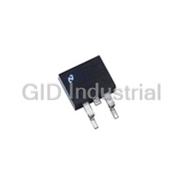
MOSFET N-CH 60V 80A TO-263AB
MOSFET N-CH 30V 31A TO-263AB
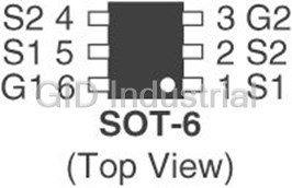
SSOT6B, COMPLEMENTARY POWER TRENCH MOSFET RoHS Compliant: Yes

IC FET DGTL N-CH DUAL 25V SSOT6
IC FET DGTL N-CH DUAL 25V SSOT6
MOSFET N-CH DUAL 20V SSOT-6


Request a Quote

The quote request has been received

Close

Facing challenges or have inquiries? Feel free to contact us!
Call Us +1-469-283-2440
What they say about us
FANTASTIC RESOURCE
One of our top priorities is maintaining our business with precision, and we are constantly looking for affiliates that can help us achieve our goal. With the aid of GID Industrial, our obsolete product management has never been more efficient. They have been a great resource to our company, and have quickly become a go-to supplier on our list!
Bucher Emhart Glass
EXCELLENT SERVICE
With our strict fundamentals and high expectations, we were surprised when we came across GID Industrial and their competitive pricing. When we approached them with our issue, they were incredibly confident in being able to provide us with a seamless solution at the best price for us. GID Industrial quickly understood our needs and provided us with excellent service, as well as fully tested product to ensure what we received would be the right fit for our company.
Fuji
HARD TO FIND A BETTER PROVIDER
Our company provides services to aid in the manufacture of technological products, such as semiconductors and flat panel displays, and often searching for distributors of obsolete product we require can waste time and money. Finding GID Industrial proved to be a great asset to our company, with cost effective solutions and superior knowledge on all of their materials, it’d be hard to find a better provider of obsolete or hard to find products.
Applied Materials
CONSISTENTLY DELIVERS QUALITY SOLUTIONS
Over the years, the equipment used in our company becomes discontinued, but they’re still of great use to us and our customers. Once these products are no longer available through the manufacturer, finding a reliable, quick supplier is a necessity, and luckily for us, GID Industrial has provided the most trustworthy, quality solutions to our obsolete component needs.
Nidec Vamco
TERRIFIC RESOURCE
This company has been a terrific help to us (I work for Trican Well Service) in sourcing the Micron Ram Memory we needed for our Siemens computers. Great service! And great pricing! I know when the product is shipping and when it will arrive, all the way through the ordering process.
Trican Well Service
GO TO SOURCE
When I can't find an obsolete part, I first call GID and they'll come up with my parts every time. Great customer service and follow up as well. Scott emails me from time to time to touch base and see if we're having trouble finding something.....which is often with our 25 yr old equipment.
ConAgra Foods