

 Manufacturers
ADVANTECH 78660
Description
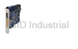
Advantech 78660 - 4-Channel 200 MHz, 16-bit A/D with Virtex-6 FPGA - x8 PCIe
Part Number
78660
Price
Request Quote
Manufacturer
ADVANTECH
Lead Time
Request Quote
Category
PRODUCTS - 7
Specifications
A/D Converters
Type: Texas Instruments ADS5485. Sampling Rate: 10 MHz to 200 MHz. Resolution: 16 bits
Clock Dividers
External clock or VCXO can be divided by 1, 2, 4, 8, or 16 for the A/D clock
Clock Synthesizer
Clock Source: Selectable from on-board programmable VCXO (10 to 810 MHz), front panel external clock or LVPECL timing bus
Synchronization: VCXO can be locked to an external 4 to 180 MHz PLL system reference, typically 10 MHz
Custom I/O Option -104
Connects 20 pairs of LVDS signals from the FPGA on PMC P14 toa 68-pin DIL ribbon-cable header on the PCIe board for custom I/O.
Custom I/O Option -105
Connects two 4X gigabitserial links from the FPGA on XMC P16 to two 4X gigabit serial connectors along the top edge of the PCIe board
External Clock
Type: Front panel female SSMC connector, sine wave, 0 to +10 dBm, AC-coupled, 50 ohms, accepts 10 to 800 MHz divider input clock or PLL system reference
External Trigger Input
Function: Programmable functions in-clude: trigger, gate, sync and PPS
Type: Front panel female SSMC connector, LVTTL
Field Programmable Gate Array
Standard: Xilinx Virtex-6 XC6VLX130T. Optional: Xilinx Virtex-6 XC6VLX240T, XC6VLX365T, XC6VSX315T, or XC6VSX475T
Front Panel Analog Signal Inputs
Input Type: Transformer-coupled, front panel female SSMC connectors. Transformer Type: Coil Craft WBC4-6TLB. Full Scale Input: +8 dBm into 50 ohms. 3 dB Passband: 300 kHz to 700 MHz
Memory
Option 150 or 160: Two 8 MB QDRII+ SRAM memory banks, 400 MHz DDR Option 155 or 165: Two 512 MB DDR3 SDRAM memory banks, 400 MHz DDR
Operating Temp
0° to 50° C
PCI-Express Interface
PCI Express Bus: Gen. 1: x4 or x8; Gen. 2: x4
Relative Humidity
0 to 95%, non-cond.
Sample Clock Sources
On-board clock
Size
Half length PCIe card, 4.38 in. x 7.13 in.
Storage Temp
–20° to 90° C
Timing Bus
26-pin front panel connector; LVPECL bus includes, clock/sync/gate/ PPS inputs and outputs; TTL signal for gate/trigger and sync/PPS inputs
Features
- Complete radar and software radio interface solution
- Four 200 MHz 16-bit A/Ds
- LVDS connections to the Virtex-6 FPGA for custom I/O
- LVPECL clock/sync bus for multiboard synchronization
- PCI Express (Gen. 1 & 2) interface up to x8
- Sample clock synchronization to an external system reference
- Supports Xilinx Virtex-6 LXT and SXT FPGAs
- Up to 2 GB of DDR3 SDRAM or 32 MB of QDRII+ SRAM
- User-configurable gigabit serial interface
Datasheet

Extracted Text
Model 78660 4-Channel 200 MHz, 16-bit A/D with Virtex-6 FPGA - x8 PCIe General Information installed functions and enable the 78660 to ® Model 78660 is a member of the Cobalt operate as a complete turnkey solution without the need to develop any FPGA IP. family of high performance PCIe boards based on the Xilinx Virtex-6 FPGA. A mul- Extendable IP Design tichannel, high-speed data converter, it is For applications that require specialized suitable for connection to HF or IF ports of a communications or radar system. Its built-in function, users can install their own custom IP for data processing. Pentek GateFlow data capture features offer an ideal turnkey FPGA Design Kits include all of the factory solution. It includes four A/Ds and four banks of installed modules as documented source code. Developers can integrate their own memory. In addition to supporting PCI Ex- IP with the Pentek factory-installed functions press Gen. 2 as a native interface, the Model 78660 includes general purpose and gigabit or use the GateFlow kit to completely replace the Pentek IP with their own. serial connectors for application-specific I/O . Xilinx Virtex-6 FPGA The Cobalt Architecture The Pentek Cobalt Architecture features The Virtex-6 FPGA can be populated with a variety of different FPGAs to match a Virtex-6 FPGA. All of the board’s data and control paths are accessible by the FPGA, the specific requirements of the processing task. Supported FPGAs include: LX130T enabling factory-installed functions including LX240T, LX365T, SX315T, or SX475T. The data multiplexing, channel selection, data packing, gating, triggering and memory SXT parts feature up to 2016 DSP48E slices and are ideal for modulation/demodulation, control. The Cobalt Architecture organizes encoding/decoding, encryption/decryption, the FPGA as a container for data processing applications where each function exists as an and channelization of the signals between transmission and reception. For applications intellectual property (IP) module. not requiring large DSP resources, one of Each member of the Cobalt family is deliv- ered with factory installed applications ideally the lower-cost LXT FPGAs can be installed. Option -104 connects 20 pairs of LVDS matched to the board’s analog interfaces. signals from the FPGA on PMC P14 to a The 78660 factory-installed functions include four A/D acquisition IP modules. 68-pin DIL ribbon-cable header on the PCIe Features board for custom I/O. IP modules for either DDR3 or QDRII+ Option -105 connects two 4X gigabit ■ Complete radar and software memories, a controller for all data clocking and synchronization functions, a test signal serial links from the FPGA on XMC P16 to radio interface solution two 4X gigabit serial connectors along the generator, an Aurora gigabit serial interface, ■ Supports Xilinx Virtex-6 top edge of the PCIe board. and a PCIe interface complete the factory- ➤ LXT and SXT FPGAs ■ Four 200 MHz 16-bit A/Ds ■ Up to 2 GB of DDR3 SDRAM RF In RF In RF In RF In or 32 MB of QDRII+ SRAM ■ Sample clock synchronization RF RF RF RF to an external system reference XFORMR XFORMR XFORMR XFORMR Sample Clk / ■ LVPECL clock/sync bus for Reference Clk In multiboard synchronization Gate / Trigger / TIMING BUS A/D Clock/Sync Bus Sync / PPS GENERATOR 200 MHz 200 MHz 200 MHz 200 MHz ■ PCI Express (Gen. 1 & 2) 16-BIT A/D 16-BIT A/D 16-BIT A/D 16-BIT A/D Clock / Sync / TTL Gate / Trig interface up to x8 Gate / PPS TTL Sync / PPS ■ User-configurable gigabit Sample Clk 16 16 16 16 Reset serial interface Gate A Gate B ■ LVDS connections to the Sync / PPS A VIRTEX-6 FPGA Sync / PPS B VCXO Virtex-6 FPGA for custom I/O LX130T, LX240T, LX365T, SX315T or SX475T Timing Bus LVDS GTX GTX GTX 16 16 16 16 16 16 16 16 16 40 8X 4X 4X QDRII+ QDRII+ QDRII+ QDRII+ Config SRAM SRAM SRAM SRAM FLASH 8MB 8MB 8MB 8MB 64 MB Optional Optional QDRII+ option 150 QDRII+ option 160 FPGA Serial x8 PCIe DDR3 option 155 DDR3 option 165 GPIO I/O DDR3 DDR3 DDR3 DDR3 Dual 4X SDRAM SDRAM SDRAM SDRAM 68-pin Serial 512 MB 512 MB 512 MB 512 MB Header Conn Memory Banks1&2 Memory Banks3&4 x8 PCI Express One Park Way ◆ Upper Saddle River ◆ New Jersey 07458 Pentek, Inc. www.pentek.com . . . . Tel: 201 818 5900 ◆ Fax: 201 818 5904 ◆ Email: info pentek.com @ New! New! New! New! New! Model 78660 4-Channel 200 MHz, 16-bit A/D with Virtex-6 FPGA - x8 PCIe ➤ ➤ A/D Converter Stage ➤ ➤ ➤ LVPECL bus can drive the timing signals The front end accepts four full-scale for synchronizing multiple boards. Multiple 78660’s can be driven from the analog HF or IF inputs on front panel SSMC connectors at +8 dBm into 50 ohms with LVPECL bus master, supporting synchronous sampling and sync functions across all con- transformer coupling into four Texas nected boards. Instruments ADS5485 200 MHz, 16-bit A/D converters. Memory Resources The digital outputs are delivered into The 78660 architecture supports up to the Virtex-6 FPGA for signal processing, data capture or for routing to other board four independent memory banks which can be configured with all QDRII+ SRAM, resources. DDR3 SDRAM, or as combination of two Clocking and Synchronization banks of each type of memory. An internal timing bus provides all tim- Each QDRII+ SRAM bank can be up to 8 MB deep and is an integral part of the ing and synchronization required by the A/D converters. It includes a clock, two board’s DMA capabilities, providing FIFO memory space for creating DMA packets. sync and two gate or trigger signals. An For applications requiring deep memory on-board clock generator receives an external sample clock from the front panel SSMC resources, DDR3 SDRAM banks can each be up to 512 MB deep. Built-in memory functions connector. This clock can be used directly include an A/D data transient capture mode by the A/D or divided by a built-in clock synthesizer circuit. and D/A waveform playback mode. In addition to the factory-installed In an alternate mode, the sample clock functions, custom user-installed IP within can be sourced from an on-board program- A/D Acquisition IP Modules mable voltage-controlled crystal oscillator. the FPGA can take advantage of the memo- ries for many other purposes. The 78660 features four A/D In this mode, the front panel SSMC connector Acquisition IP Modules for eas- can be used to provide a 10 MHz reference PCI Express Interface clock for synchronizing the internal oscillator. ily capturing and moving data. The Model 78660 includes an industry- Each IP module can receive data A front panel 26-pin LVPECL Clock/Sync standard interface fully compliant with PCI from any of the four A/Ds or a connector allows multiple boards to be synchronized. In the slave mode, it accepts Express Gen. 1 & 2 bus specifications. test signal generator Supporting PCIe links up to x8, the interface Each IP module has an asso- LVPECL inputs that drive the clock, sync includes multiple DMA controllers for ciated memory bank for buffering and gate signals. In the master mode, the efficient transfers to and from the board. data in FIFO mode or for storing ➤ data in transient capture mode. All memory banks are supported with DMA engines for easily from from from from A/D Ch 1 A/D Ch 2 A/D Ch 3 A/D Ch 4 moving A/D data through the PCIe interface. These powerful linked-list DMA engines are TEST capable of a unique Acquisition SIGNAL INPUT MULTIPLEXER GENERATOR Gate Driven mode. In this mode, the length of a transfer performed DATA DATA DATA DATA by a link definition need not be PACKING PACKING PACKING PACKING & FLOW & FLOW & FLOW & FLOW known prior to data acquisition; CONTROL CONTROL CONTROL CONTROL rather, it is governed by the length MEMORY MEMORY MEMORY MEMORY MUX MUX MUX MUX CONTROL CONTROL CONTROL CONTROL of the acquisition gate. This is to to extremely useful in applications METADATA METADATA to METADATA to METADATA Mem GENERATOR Mem GENERATOR Mem GENERATOR Mem GENERATOR where an external gate drives Bank 1 Bank 2 Bank 3 Bank 4 acquisition and the exact length LINKED-LIST LINKED-LIST LINKED-LIST LINKED-LIST DMA ENGINE DMA ENGINE DMA ENGINE DMA ENGINE of that gate is not known or is A/D A/D A/D A/D likely to vary. ACQUISITION ACQUISITION ACQUISITION ACQUISITION IP MODULE 1 IP MODULE 2 IP MODULE 3 IP MODULE 4 For each transfer, the DMA engine can automatically construct metadata packets containing A/D channel ID, a sample-accu- PCIe INTERFACE rate time stamp and data length VIRTEX-6 VIRTEX-6 FPGA FPGA D DA AT TAFLOW AFLOW D DET ETAIL AIL (supports user installed IP) information. These actions sim- plify the host processor’s job of identifying and executing on the 8X 4X 4X 40 Memory Memory Memory Memory Gigabit FPGA PCIe Bank 1 Bank 2 Bank 3 Bank 4 data. Serial I/O GPIO One Park Way ◆ Upper Saddle River ◆ New Jersey 07458 Pentek, Inc. www.pentek.com . . . . Tel: 201 818 5900 ◆ Fax: 201 818 5904 ◆ Email: info pentek.com @ Model 78660 4-Channel 200 MHz, 16-bit A/D with Virtex-6 FPGA - x8 PCIe ➤ ➤ Specifications ➤ ➤ ➤ External Trigger Input Front Panel Analog Signal Inputs Type: Front panel female SSMC connec- tor, LVTTL Input Type: Transformer-coupled, front panel female SSMC connectors Function: Programmable functions in- clude: trigger, gate, sync and PPS Transformer Type: Coil Craft Field Programmable Gate Array WBC4-6TLB Full Scale Input: +8 dBm into 50 ohms Standard: Xilinx Virtex-6 XC6VLX130T Optional: Xilinx Virtex-6 XC6VLX240T, 3 dB Passband: 300 kHz to 700 MHz XC6VLX365T, XC6VSX315T, or A/D Converters Type: Texas Instruments ADS5485 XC6VSX475T Custom I/O Sampling Rate: 10 MHz to 200 MHz Option -104: Connects 20 pairs of LVDS Resolution: 16 bits Sample Clock Sources: On-board clock signals from the FPGA on PMC P14 to a 68-pin DIL ribbon-cable header on the synthesizer PCIe board for custom I/O. Clock Synthesizer Clock Source: Selectable from on-board Option -105: Connects two 4X gigabit serial links from the FPGA on XMC P16 programmable VCXO (10 to 810 MHz), to two 4X gigabit serial connectors front panel external clock or LVPECL timing bus along the top edge of the PCIe board Memory Synchronization: VCXO can be locked Option 150 or 160: Two 8 MB QDRII+ to an external 4 to 180 MHz PLL system reference, typically 10 MHz SRAM memory banks, 400 MHz DDR Option 155 or 165: Two 512 MB DDR3 Clock Dividers: External clock or VCXO SDRAM memory banks, 400 MHz DDR can be divided by 1, 2, 4, 8, or 16 for the A/D clock PCI-Express Interface PCI Express Bus: Gen. 1: x4 or x8; External Clock Gen. 2: x4 Type: Front panel female SSMC connec- tor, sine wave, 0 to +10 dBm, AC-coupled, Environmental Operating Temp: 0° to 50° C 50 ohms, accepts 10 to 800 MHz divider Storage Temp: –20° to 90° C input clock or PLL system reference Timing Bus: 26-pin front panel connector; Relative Humidity: 0 to 95%, non-cond. Size: Half length PCIe card, 4.38 in. x 7.13 in. LVPECL bus includes, clock/sync/gate/ PPS inputs and outputs; TTL signal for gate/trigger and sync/PPS inputs Ordering Information Model Description 78660 4-Channel 200 MHz A/D with Virtex-6 FPGA - PCIe Options: -062 XC6VLX240T FPGA -063 XC6VLX365T FPGA -064 XC6VSX315T FPGA -065 XC6VSX475T FPGA -104 LVDS FPGA I/O through 68-pin ribbon cable connector -105 Gigabit serial FPGA I/O through two 4X top edge connectors -150 Two 8 MB QDRII+ SRAM Memory Banks (Banks 1 and 2) -160 Two 8 MB QDRII+ SRAM Memory Banks (Banks 3 and 4) -155 Two 512 MB DDR3 SDRAM Memory Banks (Banks 1 and 2) -165 Two 512 MB DDR3 SDRAM Memory Banks (Banks 3 and 4) One Park Way ◆ Upper Saddle River ◆ New Jersey 07458 Pentek, Inc. www.pentek.com . . . . Tel: 201 818 5900 ◆ Fax: 201 818 5904 ◆ Email: info pentek.com @ Model 78660 4-Channel 200 MHz, 16-bit A/D with Virtex-6 FPGA - x8 PCIe A/D Performance Spurious Free Dynamic Range Spurious Pick-up f = 70 MHz, f = 200 MHz, Internal Clock f = 200 MHz, Internal Clock in s s Two-Tone SFDR Two-Tone SFDR f = 30 MHz, f = 70 MHz, f = 200 MHz f = 69 MHz, f = 71 MHz, f = 200 MHz 1 2 s 1 2 s Adjacent Channel Crosstalk Crosstalk Input Frequency Response f = 200 MHz, Internal Clock f = 70 MHz, f = 200 MHz, Ch 1 shown s in Ch2 s One Park Way ◆ Upper Saddle River ◆ New Jersey 07458 Pentek, Inc. www.pentek.com . . . . Tel: 201 818 5900 ◆ Fax: 201 818 5904 ◆ Email: info pentek.com @
Frequently asked questions
What makes Elite.Parts unique?

What kind of warranty will the 78660 have?
Which carriers does Elite.Parts work with?
Will Elite.Parts sell to me even though I live outside the USA?
I have a preferred payment method. Will Elite.Parts accept it?
Why buy from GID?

Quality
We are industry veterans who take pride in our work

Protection
Avoid the dangers of risky trading in the gray market

Access
Our network of suppliers is ready and at your disposal

Savings
Maintain legacy systems to prevent costly downtime

Speed
Time is of the essence, and we are respectful of yours
Related Products

Request a Quote

The quote request has been received
Close

Facing challenges or have inquiries? Feel free to contact us!
Call Us +1-469-283-2440
What they say about us
FANTASTIC RESOURCE
One of our top priorities is maintaining our business with precision, and we are constantly looking for affiliates that can help us achieve our goal. With the aid of GID Industrial, our obsolete product management has never been more efficient. They have been a great resource to our company, and have quickly become a go-to supplier on our list!
Bucher Emhart Glass
EXCELLENT SERVICE
With our strict fundamentals and high expectations, we were surprised when we came across GID Industrial and their competitive pricing. When we approached them with our issue, they were incredibly confident in being able to provide us with a seamless solution at the best price for us. GID Industrial quickly understood our needs and provided us with excellent service, as well as fully tested product to ensure what we received would be the right fit for our company.
Fuji
HARD TO FIND A BETTER PROVIDER
Our company provides services to aid in the manufacture of technological products, such as semiconductors and flat panel displays, and often searching for distributors of obsolete product we require can waste time and money. Finding GID Industrial proved to be a great asset to our company, with cost effective solutions and superior knowledge on all of their materials, it’d be hard to find a better provider of obsolete or hard to find products.
Applied Materials
CONSISTENTLY DELIVERS QUALITY SOLUTIONS
Over the years, the equipment used in our company becomes discontinued, but they’re still of great use to us and our customers. Once these products are no longer available through the manufacturer, finding a reliable, quick supplier is a necessity, and luckily for us, GID Industrial has provided the most trustworthy, quality solutions to our obsolete component needs.
Nidec Vamco
TERRIFIC RESOURCE
This company has been a terrific help to us (I work for Trican Well Service) in sourcing the Micron Ram Memory we needed for our Siemens computers. Great service! And great pricing! I know when the product is shipping and when it will arrive, all the way through the ordering process.
Trican Well Service
GO TO SOURCE
When I can't find an obsolete part, I first call GID and they'll come up with my parts every time. Great customer service and follow up as well. Scott emails me from time to time to touch base and see if we're having trouble finding something.....which is often with our 25 yr old equipment.
ConAgra Foods