

 Manufacturers
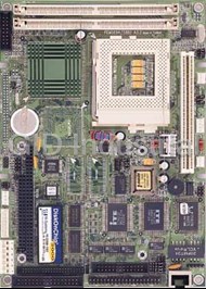
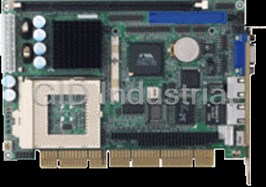
AAEON PCM-5894/5892
Description
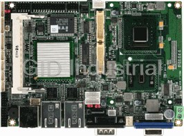
AAEON PCM-5894/5892 CPU Board. SVGA, Ethernet, 4 serial ports
Part Number
PCM-5894/5892
Price
Request Quote
Manufacturer
AAEON
Lead Time
Request Quote
Category
SINGLE BOARD COMPUTERS
Specifications
BIOS
Award FLASH BIOS
Board size
8?(L) x 5.75?(W) (203 mm x 146 mm)
Board Type
5.25 in
Chipset
SiS5582 (PCM-5892)/SiS5598(PCM-5894)
CPU
Intel Pentium MMX 166
Display memory
2MB onboard/UMA structure for PCM-5892
Display type
Supports CRT and flat panel (TFT, DSTN, Mono, and EL) display. Can display both CRT and flat panel simultaneously
DMA channels
7
Enhanced IDE hard disk drive interface
Supports up to two IDE drives. Supports PIO mode 4 and Bus Master. Also supports Multi-word DMA and Ultra DMA/33.
Ethernet controller
Realtek RTL8139 10Base-T/100Base-TX Ethernet controller
FDD interface
Supports up to two floppy disk drives.
Interrupt levels
15
Keyboard/mouse connector
8-pin connector supports standard PC/AT keyboard and PS/2 mouse.
Level 2 cache
Onboard 512KB pipeline burst L2 cache.
Multi-mode parallel port
Configured to LPT1, LPT2, LPT3, or disabled. Supports SPP, ECP, and EPP.
Operating temperature
32 to 140o F (0 to 60o C)
PC/104 connector
104-pin connector for a 16-bit bus.
Power management
I/O peripheral devices support power saving and doze/standby/suspend modes and is APM 1.2 compliant
Processor
Intel Pentium MMX
Resolution
Supports up to 1024 x 768 @ 64K colors.
Serial ports
Three RS-232 and one RS-232/422/485 serial ports. Ports can be configured as COM1, COM2, COM3, COM4, or disabled individually.
SSD interface
One 32-pin DIP socket for M-Systems DiskOnChip 2000 series, memory capacity from 2MB to 72MB.
System memory
32Mb, (supports up to 128Mb). Two 72-pin SIMM sockets onboard. Supports BEDO, EDO, and FP DRAM.
USB connectors
Two USB connectors on-board
VGA controller
C&T 65554(PCM-5894)/SiS 5598(PCM-5892)
Watchdog timer
Can generate a system reset, IRQ15 or NMI. Selectable timeout interval. (2sec~128min, 1sec/step).
Weight
0.3 kg
Features
- 10Base-T/100Base-TX Ethernet, supports remote boot ROM function
- Accepts Intel Pentium MMX 166~233MHz, AMD-K6/200~300AFR, Cyrix /IBM/6x86MX-PR166~266GP and IDT winchip C6 180~225MHz
- Bus Master IDE and Ultra DMA/33 supported
- C&T 65554 LCD controller supports 36-bit TFT panels
- DiskOnChip (SSD) up to 72MB
- Three RS-232 and one RS-232/422/485 serial port
Datasheet

Extracted Text
PCM-5894
PCM-5892
All-in-One Single Board Pentium
Computer with SVGA, Ethernet,
and 4 serial ports
FCC STATEMENT
THIS DEVICE COMPLIES WITH PART 15 FCC RULES. OPERA-
TION IS SUBJECT TO THE FOLLOWING TWO CONDITIONS:
(1) THIS DEVICE MAY NOT CAUSE HARMFUL INTERFER-
ENCE. (2) THIS DEVICE MUST ACCEPT ANY INTERFERENCE
RECEIVED INCLUDING INTERFERENCE THAT MAY CAUSE
UNDESIRED OPERATION.
THIS EQUIPMENT HAS BEEN TESTED AND FOUND TO
COMPLY WITH THE LIMITS FOR A CLASS "A" DIGITAL
DEVICE, PURSUANT TO PART 15 OF THE FCC RULES.
THESE LIMITS ARE DESIGNED TO PROVIDE REASON-
ABLE PROTECTION AGAINTST HARMFUL INTERFER-
ENCE WHEN THE EQUIPMENT IS OPERATED IN A
COMMERCIAL ENVIRONMENT. THIS EQUIPMENT GENER-
ATES, USES, AND CAN RADIATE RADIO FREQUENCY
ENERGY AND , IF NOT INSTATLLED AND USED IN ACCOR-
DANCE WITH THE INSTRUCTION MANUAL, MAY CAUSE
HARMFUL INTERFERENCE TO RADIO COMMUNICA-
TIONS. OPERATION OF THIS EQUIPMENT IN A RESIDEN-
TIAL AREA IS LIKELY TO CAUSE HARMFUL INTERFER-
ENCE IN WHICH CASE THE USER WILL BE REQUIRED
TO CORRECT THE INTERFERENCE AT HIS OWN EX-
PENSE.
Copyright Notice
This document is copyrighted, 1998. All rights are reserved. The
original manufacturer reserves the right to make improvements to
the products described in this manual at any time without notice.
No part of this manual may be reproduced, copied, translated or
transmitted in any form or by any means without the prior written
permission of the original manufacturer. Information provided in
this manual is intended to be accurate and reliable. However, the
original manufacturer assumes no responsibility for its use, nor for
any infringements upon the rights of third parties which may result
from its use.
Acknowledgements
AMD is a trademark of Advanced Micro Devices, Inc.
AMI is a trademark of American Megatrends, Inc.
Award is a trademark of Award Software International, Inc.
Cyrix is a trademark of Cyrix Corporation.
IBM, PC/AT, PS/2, and VGA are trademarks of International
Business Machines Corporation.
Intel and Pentium are trademarks of Intel Corporation.
®
Microsoft Windows is a registered trademark of Microsoft Corp.
SMC is a trademark of Standard Microsystems Corporation.
RTL is a trademark of Realtek Semi-Conductor Co., Ltd.
C&T is a trademark of Chips and Technologies, Inc.
UMC is a trademark of United Microelectronics Corporation.
ITE is a trademark of Integrated Technology Express, Inc.
SIS is a trademark of Silicon Integrated Systems Corp.
VIA is a trademark of VIA Technology, Inc.
All other product names or trademarks are properties of their
respective owners.
Part No. 2047589402 Manual PCM-5894/5892 A3.2 3rd Edition
Prepared in Taiwan Feb. 1999
Packing list
Before you begin installing your card, please make sure that the
following materials have been shipped:
• 1 PCM-5894/PCM-5892 All-in-One Single Board Computer
• 1 Quick Installation Guide
• 1 CD-ROM contains the followings:
— User’s Manual (this manual in PDF file)
— Ethernet drivers and utilities
— VGA drivers and utilities
— Latest BIOS (as of this product was shipped)
• PC/104 module mounting support kit
The PCM-5894/5892 require several cables for operation. You
can make them yourself or pruchase an optioanl cable kit, PCM-
10489-3 (P/N : 9979048900).
If any of these items are missing or damaged, contact your
distribuitor or sales representative immediately.
WARNING
The PCM-5894/5892 adopts a "P9" type power connector
for operation.
Please be advised that the PCM-5894/5892 Rev.A3 or higher
revision requires a "P9" power connector for proper operation.
On the standard PS/2 power supplies, there are usually two
similar 6-pin power plugs. P8 has one +5V output while P9 has
three. +5V is normally indicated by red color so you should be
able to distinguish P9 from P8 by counting the number of red
wire. Many times, there are also markings on these two plugs
indicating which is which.
P9 CONNECTOR
P1 IN NO.P2IN-P3 IN-P4 IN-P5 IN-P6 IN-PIN-
SD ignalGDN GV N -V 5 +V5 +V5 +5
Ck olorBklacBe lacWdhit Rd e Rd e Re
NOTE : Without any aditional devices, PCM-5894/5892
alone is +5V operational. -5V of P9 power
connector is not required.
** PLEASE be absolutely certain that you are using the correct
plug before continuing.
Contents
Chapter 1: General Information .......................... 1
Introduction ............................................................................ 2
Onboard peripherals with true PCI performance ................ 2
Features ................................................................................... 3
Specifications .......................................................................... 4
Standard SBC functions ............................................................ 4
Board layout ........................................................................... 6
Board dimensions ................................................................... 7
Chapter 2: Installation ......................................... 9
Jumpers and connectors ...................................................... 10
Locating jumpers .................................................................. 12
Locating connectors ............................................................. 13
Setting jumpers ..................................................................... 14
CPU installing and upgrading ............................................. 15
Installing DRAM (SIMMs) .................................................. 16
Installing SIMMs .................................................................. 16
Internal VGA setting (J1)
(for PCM-5892 chipset only)............................................. 17
System clock setting (J2)................................................... 18
LCD driving voltage select (J3 and J11) ........................ 19
LCD singal select (J5)(J6) ................................................ 19
Clear CMOS (J7)................................................................ 19
CPU frequency ratio (J8) ................................................... 20
CPU type select (J10) ........................................................ 21
CPU voltage setting (J12) ................................................. 22
DOC address selection (J13 ............................................. 23
Ethernet LED signal connectors (J14, J15, J16) ................ 24
COM2 RS-232/422/485 select .............................................. 25
COM3/COM4 IRQ select ..................................................... 25
COM3/COM4 RI pin voltage select (J20, J21) .................. 26
Display connectors (CN1, CN3) .......................................... 27
USB connector (CN5) ........................................................... 29
Front panel connector (CN6) ............................................... 30
Power connectors (CN8, CN12, CN2, CN17, and CN19) .. 31
Keyboard and mouse connector (CN9) .............................. 32
IDE hard drive connector (CN11) ....................................... 33
connecting the hard drive ........................................................ 33
IDE hard drive connector (CN11)........................................... 34
Parallel port connector (CN13) ........................................... 35
Parallel port IRQ ..................................................................... 35
Parallel port connector table (CN13) ...................................... 35
Serial ports (CN15) ............................................................... 36
COM 1-4 RS-232/422/485 serial ports (CN15) ...................... 36
Floppy drive connector (CN16) ........................................... 37
Connecting the floppy drive .................................................... 37
Floppy drive connector (CN16) .............................................. 38
DiskOnChip socket (U16) .................................................... 39
DiskOnChip (DOC) 2000 Installation ................................ 40
CPU jumper setting example ............................................... 41
Chapter 3: AMIBIOS Setup .................................. 47
System test and initialization ............................................... 48
System configuration verification ............................................ 48
Award BIOS setup ................................................................ 49
Entering setup ......................................................................... 49
Standard CMOS Setup ........................................................ 51
BIOS features setup .............................................................. 53
CHIPSET features setup ...................................................... 57
Power management setup .................................................... 61
PNP/PCI configuration setup .............................................. 67
Load BIOS defaults/Load setup defaults ........................... 70
Integrated peripherals setup ................................................ 71
Supervisor/User password setting ........................................ 69
IDE HDD auto detect ........................................................... 71
Hdd low level format utility ................................................. 78
Save & exit setup .................................................................. 79
Exit without saving ............................................................... 81
Chapter 4: C&T 6555x Flat Panel/CRT controller
Display Drivers and Utilities (For
PCM-5894only)................................81
Software Drives ................................................................... 82
Hardware configuration .......................................................... 82
Necessary prerequisites ..........................................................83
Before you begin .....................................................................83
Windows 95 .......................................................................... 84
Driver installation .................................................................... 84
Windows 3.1......................................................................... 85
Driver installation .................................................................... 85
OS/2 ....................................................................................... 86
Windows NT 3.51................................................................ 88
Windows NT 4.0 .................................................................. 89
Chapter 5: SiS 5598 VGA Drivers (For PCM-5892
only) ................................................91
System Requirements ........................................................ 92
Windows 95 .......................................................................... 92
WINDOWS 95 (Display driver installation) .................... 92
Selecting resolution, color depth, and refresh ............... 93
Windows 3.x......................................................................... 94
Installation ...............................................................................94
Craphics setup .........................................................................94
Power saving setup in Windows 3.x........................................95
NT 3.5x ................................................................................. 95
Windows NT 3.5x display drivers installation .......................... 95
Selecting resolution and color depth ...........................................
NT 4.0 ................................................................................... 96
Windows NT 4.0 display drivers installation ............................ 96
Selecting resolution and color depth ........................................ 97
DOS ....................................................................................... 98
VGA utility .............................................................................. 98
Video mode setting .................................................................. 98
Frame Rate setting .................................................................. 98
Power saving setting ............................................................... 98
Chapter 6: Ethernet Software configuration... 99
Ethernet software configuration ........................................ 100
Appendix A: Programming the Watchdog Timer .
....................................................... 101
Programming the watchdog timer ..................................... 102
How to program the WATCHDOG TIMER ......................... 102
Demo program ...................................................................... 103
Appendix B: Installing PC/104 Modules ........... 105
Installing PC/104 modules .................................................... 106
Appendix C: Optional Extras ............................ 109
PCM-10489-3 Cable kit for PCM-5894 ................................ 110
1
General
Information
This chapter gives background informa-
tion on the mainboard.
Sections include:
• Board specifications
• Layout and dimensions
Chapter 1 General Information 1
CHAPTER
Introduction
The PCM-5894/5892 is a Pentium single board computer with
one onboard PCI SVGA controller, one PCI Ethernet interface
and one PCI expansion slot. Equipped with a 64-bits local bus
architecture, the PCM-5894/5892 releases Pentium's full
potential and provides unprecedented performance compared to
current 32-bit processor boards. The PCM-5894/5892 offers all
the functions of an industrial computer on a single board, but fits
in the space of a 5¼" floppy drive (only 5.75" x 8"). For maximum
performance, the PCM-5894/5892 also supports a 512 KB. L2
cache onboard. An SSD interface supports one 32-pin DIP socket
for the M-Systems DiskOnChip 2000 series, memory capacity
from 2MB to 72MB.
Onboard features include four serial ports (three RS-232 and one
RS-232/422/485), one multi-mode parallel (ECP/EPP/SPP) port, one
floppy drive controller and one keyboard/PS-2 mouse interface.
The built-in high speed PCI IDE controller supports both PIO and
bus master modes. Up to two IDE devices can be connected,
including large hard disks, CD-ROM drives, tape backup drives,
and other IDE devices.
The PCM-5894/5892 also features power management to minimize
power consumption. It complies with the “Green Function”
standard and supports three types of power saving features: Doze
mode, Standby mode, and Suspend mode. In addition, the board’s
watchdog timer can automatically reset the system or generate an
interrupt in case the system stops due to a program bug or EMI.
Onboard peripherals with true PCI
performance
The PCM-5894/5892 is a highly integrated, all-in-one single board
computer. All onboard peripherals (including PCI flat panel/VGA
interface, PCI Ethernet, and PCI IDE) adopt PCI technology and
operate through an internal PCI bus. Integrating a Pentium board
with a PCI architecture has unleashed a revolutionary level of
performance. The PCM-5894/5892 is one of the smallest and
most powerful all-in-one Pentium boards available.
2 PCM-5894/5892 User Manual
Features
• Accepts Intel Pentium MMX 166~233MHz, AMD-K6/200~300AFR,
Cyrix /IBM/6x86MX-PR166~266GP and IDT winchip C6 180~225MHz
• DiskOnChip (SSD) up to 72MB
• C&T 65554 LCD controller supports 36-bit TFT panels
• 10Base-T/100Base-TX Ethernet, supports remote boot ROM function
• Bus Master IDE and Ultra DMA/33 supported
• Three RS-232 and one RS-232/422/485 serial port
Chapter 1 General Information 3
Specifications
Standard SBC functions
• CPU: Intel Pentium MMX 166~233MHz, AMD-K6/200~266AFR,
Cyrix /IBM/6x86MX-PR166~266GP and IDT winchip C6
180~225MHz
• BIOS: Award FLASH BIOS
• Chipset: SiS5582 (PCM-5892)/SiS5598(PCM-5894)
• Level 2 cache: Onboard 512KB pipeline burst L2 cache.
• System memory: 8MB to 128MB. Two 72-pin SIMM sockets
onboard. Supports BEDO, EDO, and FP DRAM.
• DMA channels: 7
• Interrupt levels: 15
• Enhanced IDE hard disk drive interface: Supports up to two IDE drives.
Supports PIO mode 4 and Bus Master. Also supports Multi-word DMA
and Ultra DMA/33.
• FDD interface: Supports up to two floppy disk drives.
• Multi-mode parallel port: Configured to LPT1, LPT2, LPT3, or disabled.
Supports SPP, ECP, and EPP.
• Serial ports: Three RS-232 and one RS-232/422/485 serial ports. Ports
can be configured as COM1, COM2, COM3, COM4, or disabled individ-
ually. Four 16C550 serial UARTs. IR connector reserved for future use.
• Keyboard/mouse connector: 8-pin connector supports standard PC/AT
keyboard and PS/2 mouse.
• USB connectors: Two USB connectors on-board
• Watchdog timer: Can generate a system reset, IRQ15 or NMI. Selectable
timeout interval. (2sec~128min, 1sec/step).
• Power management: I/O peripheral devices support power saving and
doze/standby/suspend modes and is APM 1.2 compliant
4 PCM-5894/5892 User Manual
• VGA controller: C&T 65554(PCM-5894)/SiS 5598(PCM-5892)
• Display memory: 2MB onboard/UMA structure for PCM-5892
• Display type: Supports CRT and flat panel (TFT, DSTN, Mono, and
EL) display. Can display both CRT and flat panel simultaneously
(PCM-5892 supports CRT displays only)
• Resolution: Supports up to 1024 x 768 @ 64K colors.
• Ethernet controller: Realtek RTL8139 10Base-T/100Base-TX Ethernet
controller
• SSD interface: One 32-pin DIP socket for M-Systems DiskOnChip 2000
series, memory capacity from 2MB to 72MB.
• PC/104 connector: 104-pin connector for a 16-bit bus.
• Power supply voltage: +5V (4.75V to 5.25V)
+12V (11.4V to 12.6V)
• Power requirements:
Bare Board: +5V @ 1.5A
Pentium MMX-233 onboard: +5V @ 6A
AMD K6-233 onboard: +5V @ 10A
o o
• Operating temperature: 32 to 140 F (0 to 60 C)
• Board size: 8”(L) x 5.75”(W) (203 mm x 146 mm)
• Weight: 0.3 kg
Chapter 1 General Information 5
iTE
IT8661F
Board layout
BAT
CHIPS
B5554
6 PCM-5894/5892 User Manual
RTL8139
UMC
UM8663BF
U1
DiskOnChip
SiS
5598/5582
20PMT04A
Board dimensions
5.08
3.56
40.64
97.16
100.97
119.38
174.63
177.17
193.04
198.12
203.20
Dimensions in mm
PCM-5894/5892 dimensions
Chapter 1 General Information 7
5.08
9.53
95.25
135.89
140.97
146.05
8 PCM-5894/5892 User Manual
2
Installation
This chapter describes how to set up the
main board hardware, including instruc-
tions on setting jumpers and connecting
peripherals, switches, and indicators. Be
sure to read all the safety precautions
before you begin the installation proce-
dure.
Chapter 2 Installation 9
CHAPTER
Jumpers and connectors
Connectors on the board link it to external devices such as hard
disk drives, a keyboard, or floppy drives. In addition, the board
has a number of jumpers that allow you to configure your system
to suit your application.
The table below lists the function of each of the board's jumpers
and connectors.
Jumpers
Label Function
J1 Internal VGA setting
J2 System clock setting
J3 LCD driving voltage select
J5 LCD SHF clock setting
J6 LCD ASHF clock setting
J7 Clear CMOS
J8 CPU frequency ratio
J10 CPU type select
J11 LCD driving voltage select
J12 CPU voltage setting
J13 DOC address select
J14 Ethernet transmitting LED
J15 Ethernet receiving LED
J16 Ethernet link signal LED
J17 COM2 selection
J18 COM2 selection
J19 IRQ selection (COM3, COM4)
J20 COM3 RI Pin voltage select
J21 COM4 RI Pin voltage select
10 PCM-5894/5892 User Manual
Connectors
Label Function
CN1 VGA display connector
CN2 Fan power connector
CN3 LCD display connector
CN5 USB connector
CN6 Front panel connector
CN8 Auxilliary power connector (+5V, +12V)
CN9 Keyboard and mouse connector
CN10 IrDA connector
CN11 IDE hard drive connector
CN12 Main power connector
CN13 Printer port connector
CN14 Ethernet 100/10Base-T connector
CN15 Serial port (RS-232/422/485) connectors
CN16 Floppy drive connector
CN17 Fan power connector
CN19 Auxilliary power connector (-5V, -12V)
U16 DiskOnChip socket
Chapter 2 Installation 11
Locating jumpers
J21 J20
J18
J17
J19
J16
J13
J15
J14
J11
J12
J10
J8
J7
J5
J6
J3
J2
J1
12 PCM-5894/5892 User Manual
U1
iTE
IT8661F
Locating connectors
CN16
CN14 CN15 CN13 CN11
CN12
CN10
U16
CN9
CN8
CN5
CN6
CN17
BAT
CHIPS
B5554
CN3
CN19
CN2
CN1
Chapter 2 Installation 13
RTL8139
UMC
UM8663BF
U1
DiskOnChip
SiS
5598/5582
20PMT04A
Setting jumpers
You configure your card to match the needs of your application by
setting jumpers. A jumper is the simplest kind of electric switch.
It consists of two metal pins and a small metal clip (often
protected by a plastic cover) that slides over the pins to connect
them. To “close” a jumper you connect the pins with the clip. To
“open” a jumper you remove the clip. Sometimes a jumper will
have three pins, labeled 1, 2, and 3. In this case you would connect
either pins 1 and 2 or 2 and 3.
3
2
1
Open Closed Closed 2-3
The jumper settings are schematically depicted in this manual as
follows:
1 2 3
Open Closed Closed 2-3
A pair of needle-nose pliers may be helpful when working with
jumpers.
If you have any doubts about the best hardware configuration for
your application, contact your local distributor or sales represen-
tative before you make any changes.
14 PCM-5894/5892 User Manual
CPU installing and upgrading
You can upgrade to a more powerful Pentium CPU or compatible at
any time. Simply remove the old CPU, install the new one, and set
the jumpers for the new CPU type and speed.
Warning! Always disconnect the power cord from your
chassis when you are working on it. Do not
make connections while the power is on as
sensitive electronic components can be dam-
aged by the sudden rush of power. Only experi-
enced electronics personnel should open the PC
chassis.
Caution! Always ground yourself to remove any static
charge before touching the PC board. Modern
electronic devices are very sensitive to static
electric charges. Use a grounding wrist strap at
all times. Place all electronic components on a
static-dissipative surface or in a static-shielded
bag when they are not in the chassis.
When you install a new CPU, be sure to adjust the board settings,
such as CPU type and CPU clock. Improper settings may damage
the CPU.
Chapter 2 Installation 15
Installing DRAM (SIMMs)
The PCM-5894/5892 provides two 72-pin SIMM (Single In-line
Memory Module) sockets. The SIMM supports either Fast Page
Mode (FPM) or Extended Data Output (EDO) DRAM with a
speed of at least 70 ns. Depending on the combinations of the
modules you use, you can install from 4 MB to 128 MB of RAM.
Installing SIMMs
NOTE 1: Pentium or compatible processors adopt 64 bit data
bus. Since 72-pin SIMM can only provide 32 bit data
bus width, two SIMM modules are required as one
memory bank, and both SIMMs must be the same size
and type.
1. Ensure that all power sources are disconnected.
2. Slip the memory module into the socket at a 45 degree angle.
3. Push the module toward the vertical posts at both ends of the
socket until the module is upright and the retaining clips at
both ends of the module click into place. When positioned
correctly, the pins on top of the vertical posts should corre-
spond to the circular holes on the ends of the module.
4. Repeat steps 2 and 3 for each module you install.
NOTE 2: Do not insert any SIMM module that contains more
than 24 memory chips. SIMMs contain more than 24
chips exceed the driving capability of new generation
chipsets.
16 PCM-5894/5892 User Manual
Internal VGA setting (J1)
(for PCM-5892 chipset only)
This jumpers is reserved for factory use. The PCM-5894 & PCM-
5892 use different VGA chipset, this jumper is used to select the
relative onboard VGA chipset.
Internal VGA setting (J1)
PCM-5894(SiS5582) PCM-5892(SiS5598)
1 2 3
1 2 3
JP1
7 8 9
7 8 9
Chapter 2 Installation 17
System clock setting (J2)
J2 is used to sychronize the system clock with the CPU clock and
PCI clock. You may need to adjust the CPU clock according to the
base CPU speed.
CPU clock setting
PCI J2 CPU
1 3 5
55MHz
27.5MHz
2 4 6
1 3 5
75MHz
32MHz
2 4 6
1 3 5
50MHz
33.3MHz
2 4 6
1 3 5
50MHz
25MHZ
2 4 6
1 3 5
60MHz
30MHz
2 4 6
1 3 5
* 66MHz
33MHz
2 4 6
1 3 5
40MHz
32MHz
2 4 6
* default setting
18 PCM-5894/5892 User Manual
LCD driving voltage select (J3 and
J11)
You can select the LCD connector CN3 (pin 5 and pin 6) driving
voltage by setting J3 and J11. The configuration as follows:
LCD driving voltage select (J3 and J11)
5V* 3.3V
J3
1 2 3
1 2 3
J11
1 2 3
1 2 3
*default
LCD singal select (J5)(J6)
You can select the LCD control signal by setting (J5) & (J6). The
following charts show the available option.
LCD Signal select (J5)(J6)
SHF CLK ASHF CLK
J5
J6
Clear CMOS (J7)
You can use J7 to clear the CMOS data if necessary. To reset the
CMOS data, set J7 to 2-3 closed for just a few seconds, and then
move the jumper back to 1-2 closed.
Clear CMOS (J7)
Protect (default) Clear CMOS
1 2 3
1 2 3
Chapter 2 Installation 19
CPU frequency ratio (J8)
CPU frequency ratio (J8)
J8 P54C P55C AMD-K6
1.5 3.5 3.5
1 3 5
2 4 6
2.0 2.0 2.0
1 3 5
2 4 6
2.5 2.5 2.5
1 3 5
2 4 6
3.0 3.0 3.0
1 3 5
2 4 6
(default setting)
4.0
1 3 5
2 4 6
4.5
1 3 5
2 4 6
5.5
1 3 5
2 4 6
5.0
1 3 5
2 4 6
20 PCM-5894/5892 User Manual
CPU type select (J10)
J10 must be set to match the CPU type between Dual-Voltage ( e.g.,
P55C ) and Single-Voltage ( e.g., P54C ) type CPU. The chart below
shows the proper jumper setting for their respective CPU type.
CPU type select (J10)
Dual-Voltage* Single-Voltage
J10
2 4 6
2 4 6
1 3 5
1 3 5
* default setting
Chapter 2 Installation 21
CPU voltage setting (J12)
J12 must be set to match the CPU type. The chart below shows the
proper jumper settings for the respective Vcc.
CPU voltage setting
3.6v 3.5v 3.4v
8 2 8 2 8 2
7 1 7 1
7 1
3.3v 3.2v 3.1v
8 2 8 2 8 2
7 1
7 1 7 1
3.0v 2.9v 2.8v*
*
8 2 8 2
8 2
7 1 7 1 7 1
2.7v 2.6v 2.5v
8 2 8 2 8 2
7 1
7 1 7 1
2.4v 2.3v 2.2V
8 2
8 2 8 2
7 1
7 1 7 1
2.1v
8 2
7 1
*default setting
22 PCM-5894/5892 User Manual
DOC address selection (J13)
The DiskOnChip 2000 occupies an 8 Kbyte window in the upper
memory address range of C800 to E000. You should ensure this
does not conflict with any other device's memory address. J13
controls the memory address of the Flash disk.
DiskOnChip 2000 memory address (J13)
Memory address (HEX) J13
DISABLE
5 6
3 4
1 2
DC00*
5 6
3 4
1 2
D400
5 6
3 4
1 2
D000
5 6
3 4
1 2
CC00
5 6
3 4
1 2
D800
5 6
3 4
1 2
* default setting
These addresses might conflict with the ROM BIOS of other
peripheral boards. Please select the appropriate memory address
to avoid memory conflicts.
Chapter 2 Installation 23
Ethernet LED signal connectors
(J14, J15, J16)
The PCM-5894/5892 supports three sets of LED connectors for
external LEDs.
Ethernet active signal LED (J14)(J15)
Flashing LEDs indicate that the PCM-5894/5892 is transmitting
(J14) or receiving (J15) data.
Ethernet link signal LED (J16)
A continuously lit LED indicates good linkage between the
PCM-5894/5892 and its supporting hub.
24 PCM-5894/5892 User Manual
COM2 RS-232/422/485 select
COM2 Select (J17, J18)
*RS-232 RS-422 RS-485
5
6 5 5
* 6 6
3 3 3
J17 4 4 4
1
2 1 1
2 2
3 3 3
J18 2 2 2
1 1 1
*default
COM3/COM4 IRQ select
IRQ Selection (J19)
*COM3:IRQ5 and COM4:IRQ10 COM3:IRQ10 and COM4:IRQ5
5
* 5 6 6
3
3 4
4
1 1 2
2
* default
Chapter 2 Installation 25
COM3/COM4 RI pin voltage select
(J20, J21)
COM3 RI pin setting (J20)
RI* +5V +12V
5
5 5 6 6
6
3
J20 3 3 4
4 4
1 1
1 2 2
2
COM4 RI pin setting (J21)
RI* +5V +12V
5 6 5 6 5 6
J21 3 3 3
4 4 4
1 1 1
2 2 2
26 PCM-5894/5892 User Manual
Display connectors (CN1, CN3)
The mainboard's PCI SVGA interface can drive conventional CRT
displays and is capable of driving a wide range of flat panel
displays, including electroluminescent (EL), gas plasma, passive
LCD, and active LCD displays. The card has two connectors to
support these displays, one for standard CRT VGA monitors and
one for flat panel displays.
VGA display connector (CN1)
CN1 is a 16-pin, dual-in-line header used for conventional CRT
displays. A simple one-to-one adapter can be used to match CN1 to
a standard 15-pin D-SUB connector commonly used for VGA.
VGA display connector (CN1)
Pin Signal Pin Signal
1 RED 9 SIGNAL GND
2 N/C 10 H-SYNC
3 GREEN 11 CHASSIS GND
4 SIGNAL GND 12 V-SYNC
5 BLUE 13 CHASSIS GND
6 N/C 14 N/C
7 N/C 15 CHASSIS GND
8 N/C 16 N/C
When the mainboard's power is applied, the control signal is low
until just after the relevant flat panel signals are present.
Configuration of the VGA interface is done completely via the
software utility. You don't have to set any jumpers.
Chapter 2 Installation 27
LCD connector (CN3)
Pin Signal Pin Signal
1 +12 V 2 +12 V
DC DC
3 GND 4 GND
5 +5 V 6 +5 V
DC DC
7 ENAVEE 8 GND
9P0 10 P1
11 P2 12 P3
13 P4 14 P5
15 P6 16 P7
17 P8 18 P9
19 P10 20 P11
21 P12 22 P13
23 P14 24 P15
25 P16 26 P17
27 P18 28 P19
29 P20 30 P21
31 P22 32 P23
33 P24 34 P25
35 SHF CLK 36 FLM (V SYS)
37 M 38 LP (H SYS)
39 GND 40 ENABKL
41 P26 42 P27
43 P28 44 P29
45 P30 46 P31
47 P32 48 P33
49 P34 50 P35
28 PCM-5894/5892 User Manual
USB Connector (CN5)
The PCM-5894/5892 provides two USB (Universal Serial Bus)
interfaces, which give complete plug and play, hot affach/detach
for up to 127 external devices. The USB interfaces comply with
USB specification Rev. 1.0, and can be disabled in the system
BIOS setup.
USB connector (CN5)
Pin Function Pin Function
1 Vcc 5 Vcc
2 UD1- 6 UD0-
3 UD1+ 7 UD0+
4 GND 8 GND
Chapter 2 Installation 29
Front panel connector (CN6)
Next you may want to install external switches to monitor and
control the mainboard. These features are completely optional —
install them only if you need them. The front panel connector
(CN6) is an 8-pin male, dual in-line header and provides connec-
tions for a speaker, hard disk access indicator and an input switch
for resetting the card.
Front panel connector (CN6)
Pin Signal
1 HDD LED- (Hard disk active)
2 HDD LED+ (V )
CC
3 Speaker+
4 Speaker- (GND)
5 GND
6 NC
7 Reset switch- (GND)
8 Reset switch+
Speaker
The mainboard can drive an 8W external speaker at 0.5 watts. If
there is no external speaker, the PCM-5894/5892 provides an
on-board buzzer as an alternative.
LED interface
The front panel LED indicator for hard disk access is an active low
signal (24 mA sink rate).
30 PCM-5894/5892 User Manual
Power connectors (CN8, CN12, CN2,
CN17, and CN19)
Auxilliary power connector (CN8)
CN8 supplies additional power to devices which require +5V and
+12V power.
Auxilliary power connector (CN8)
Pin Function
1 +12V
2 GND
3 GND
4 +5 V
Main power connector (CN12)
Main power connector (CN12)
Pin Signal
1 GND
2 GND
3 N/C
4 +5 V
5 +5 V
6 +5 V
Fan power connector (CN2 and CN17)
Provides power supply to an optional CPU cooling fan. Only
present when +5 V and +12 V power is supplied to the board.
Fan power connector (CN2 & CN7)
Pin Signal
1 +5 V
2 GND
3 +12 V
Chapter 2 Installation 31
Auxilliary power connector (CN19)
CN19 supplies additional power to devices which require -5V and -
12V power.
Auxilliary power connector (CN19)
Pin Function
1 GND
2 -5V
3 GND
4 -12V
Keyboard and mouse connector (CN9)
The mainboard provides a keyboard connector which supports
both a keyboard and a PS/2 style mouse. In most cases, especially
in embedded applications, a keyboard is not used. The standard
PC/AT BIOS will report an error or fail during power-on self-test
(POST) after a reset if the keyboard is not present. The mainboard
BIOS Advanced setup menu allows you to select "System Key-
board" under the "Present" or "Absent" selection. This allows no-
keyboard operation in embedded system applications without the
system halting under POST (power-on-self-test).
Keyboard and mouse connector (CN9)
Pin Signal
1 GND
2 MS V
CC
3 MS DATA
4 MS CLOCK
5 GND
6 KB V
CC
7 KB DATA
8 KB CLOCK
32 PCM-5894/5892 User Manual
IDE hard drive connector (CN11)
You can attach one or two Enhanced Integrated Device Electron-
ics hard disk drives to the mainboard's internal controller. The
mainboard's IDE controller uses a PCI local-bus interface. This
advanced interface supports faster data transfer and allows the IDE
hard drive to exceed 528 MB.
Connecting the hard drive
Connecting drives is done in a daisy-chain fashion and requires
one of two cables, depending on the drive size. 1.8" and 2.5"
drives need a 1 x 44-pin to 2 x 44-pin flat-cable connector. 3.5"
drives use a 1 x 44-pin to 2 x 40-pin connect.
Wire number 1 on the cable is red or blue, and the other wires are
gray.
1. Connect one end of the cable to CN11. Make sure that the red
(or blue) wire corresponds to pin 1 on the connector, which is
labeled on the board (on the right side).
2. Plug the other end of the cable to the Enhanced IDE hard
drive, with pin 1on the cable corresponding to pin 1 on the
hard drives. (see your hard drive's documentation for the
location of the connector).
Connect a second drive as described above.
Unlike floppy drives, IDE hard drives can connect to either
end of the cable. If you install two drives, you will need to set
one as the master and one as the slave by using jumpers on the
drives. If you install just one drive, set it as the master.
Chapter 2 Installation 33
IDE hard drive connector (CN11)
IDE hard drive connector (CN11)
Pin Signal Pin Signal
1 IDE RESET 2 GND
3DATA 7 4 DATA 8
5DATA 6 6 DATA 9
7DATA 5 8 DATA 10
9 DATA 4 10 DATA 11
11 DATA 3 12 DATA 12
13 DATA 2 14 DATA 13
15 DATA 1 16 DATA 14
17 DATA 0 18 DATA 15
19 SIGNAL GND 20 N/C
21 N/C 22 GND
23 IO WRITE 24 GND
25 IO READ 26 GND
27 IO CHANNEL READY 28 ALE
29 N/C 30 GND
31 IRQ14 32 IOCS16
33 ADDR 1 34 N/C
35 ADDR 0 36 ADDR 2
37 HARD DISK SELECT 0 38 HARD DISK SELECT 1
39 IDE ACTIVE 40 MGND
41 VCC 42 MVCC
43 GND 44 N/C
34 PCM-5894/5892 User Manual
Parallel port connector (CN13)
Normally, the parallel port is used to connect the card to a printer.
The mainboard includes an onboard parallel port, accessed through
CN13, a 26-pin flat-cable connector. You need an adapter cable if
you use a traditional DB-25 connector. The cable has a 26-pin
connector on one end and a DB-25 connector on the other.
Parallel port IRQ
The mainbaord supports one parallel port. The port is designated
as LPT1 and can be disabled or changed to LPT2 or LPT3 in the
system BIOS setup.
Parallel port connector table (CN13)
Parallel port connector (CN13)
Pin Signal Pin Signal
1 /STROBE 2 \AUTOFD
3 DO 4 ERR
5 D1 6 \INIT
7 D2 8 \SLCTINI
9 D3 10 GND
11 D4 12 GND
13 D5 14 GND
15 D6 16 GND
17 D7 18 GND
19 \ACK 20 GND
21 BUST 22 GND
23 PE 24 GND
25 SLCT 26 N/C
Chapter 2 Installation 35
Serial ports (CN15)
The mainboard offers four serial ports: three RS-232 and one RS-
232/422/485. These ports allow you to connect them to serial
devices (mouse, printers, etc.).
COM 1-4 RS-232/422/485 serial ports (CN15)
COM1, COM2, COM3, COM4 RS-232/422/485 serial port
PIN SIGNAL PIN SIGNAL
COM1 1 DCDA 2 DSRA
3 RXDA 4 RTSA
5 TXDA 6 CTSA
7 DTRA 8 RIA
9 GND 10 N.C.
COM2 11 DCDB 12 DSRB
(422TXD-/485DATA-)
13 RXDB 14 RTSB
(422TXD+/485DATA+)
15 TXDB 16 CTSB
(422RXD+)
17 DTRB 18 RIB
(422RXD-)
19 GND 20 N.C.
COM3 21 DCDC 22 DSRC
23 RXDC 24 RTSC
25 TXDC 26 CTSC
27 DTRC 28 RIC/+5V/+12V
29 GND 30 N.C.
COM4 31 DCDD 32 RSRD
33 RXDD 34 RTSD
35 TXDD 36 CTSD
37 DTRD 38 RID/+5V/+12V
39 GND 40 N.C.
36 PCM-5894/5892 User Manual
Floppy drive connector (CN16)
You can attach up to two floppy disks to the mainboard controller.
You can use any combination of 5¼" (360 KB and 1.2 MB) and/or
3½" (720 KB, 1.44 MB, and 2.88 MB) drives.
A 34-pin daisy-chain drive connector cable is required for a dual-
drive system. On 1 end of the cable is a 34-pin flat-cable connector.
On the other end are two sets of floppy disk drive connectors. Each
set consists of a 34-pin flat-cable connector (usually used for 3½"
drives) and a printed-circuit board connector (usually used for 5¼"
drives).
Connecting the floppy drive
1. Plug the 34-pin flat-cable connector into CN16. Make sure that
the red wire corresponds to pin 1 on the connector.
2. Attach the appropriate connector on the other end of the cable
to the floppy drive(s). You can use only one connector in the
set. The set on the end (after the twist in the cable) connects to
the A: drive. The set in the middle connects to the B: drive.
3. If you are connecting a 5¼" floppy drive, line up the slot in the
printed circuit board with the blocked-off part of the cable
connector.
If you are connecting a 3½" floppy drive, you may have trouble
determining which pin is pin number 1. Look for a number
printed on the circuit board indicating pin number 1. Also,
the connector on the floppy drive connector may have a slot.
When the slot is up, pin number 1 should be on the right.
Check the documentation that came with the drive for more
information.
If you desire, connect the B: drive to the connectors in the
middle of the cable as described above.
Chapter 2 Installation 37
Floppy drive connector (CN16)
Floppy drive connector (CN16)
Pin Signal Pin Signal
1 GND 2 DENSITY SELECT
3 GND 4 N/C
5 GND 6 DRIVE TYPE
7 GND 8 INDEX
9 GND 10 MOTOR 0
11 GND 12 DRIVE SELECT 1
13 GND 14 DRIVE SELECT 2
15 GND 16 MOTOR 1
17 GND 18 DIRECTION
19 GND 20 STEP
21 GND 22 WRITE DATA
23 GND 24 WRITE GATE
25 GND 26 TRACK 0
27 GND 28 WRITE PROTECT
29 GND 30 READ DATA
31 GND 32 HEAD DELECT
33 GND 34 DISK CHANGE
38 PCM-5894/5892 User Manual
DiskOnChip socket (U16)
The DiskOnChip 2000 family of products provides a single chip
solid-state flash disk in a standard 32-pin DIP package. The
DiskOnChip 2000 is a solid-state disk with no moving parts,
resulting in a significant reduction in power consumption and an
increase in reliability. The DiskOnChip is a small plug and play
Flash disk. It is easy to use. And it saves integration overhead.
The DiskOnChip 2000 family of products is available in capacities
ranging from 2MB up to 72MB, unformatted. In order to manage
the disk, the DiskOnChip 2000 includes the TrueFFS, M-Systems
Flash File System proprietary software. The DiskOnChip 2000
package is pin-to-pin compatible with a standard 32-pin EPROM
device.
pin
Description Pin Number Direction Note
Name
A0-A12 Address bus 4-12,23,25-27 Inputs
A13-A16 Address bus 2,3,28,29 Inputs 1
D0-D7 Data bus 13-15,17-21 I/O
CE/ Chip Enable 22 Input
OE /
OE/ Output Enable 24 Input
WE/ Write Enable 31 Input
NC Not connected 1.30 2
VCC Power 32
GND Ground 16
Note 1: Pins A13 through A16 are not used
by the MD2200. They are kept for socket
backward compatibility with ED 1100
(DiskOnChip 1000)
Note 2: Pins 1 and 30 are not used by
MD2200
Chapter 2 Installation 39
DiskOnChip (DOC) 2000 Installation
When the DOC is installed correctly, a DOC will work like an HDD
or an FDD. To install the DOC on the mainboard, follow the
instructions below:
1. Plug the DOC into the socket. Make sure pin 1 of the DOC is
aligned with pin 1 of the socket.
2. Push the DOC into the socket until it is firmly seated in the
socket.
Caution: the DOC may be permanently damage if it is installed
incorrectly.
3. Set the jumper for the memory address of the DOC.
Note:
The memory shadow function sometimes will create conflicts with
the memory window. You should disable the memory shadow from
the BIOS SETUP if the DOC cannot be accessed.
Configure DOC as a boot device
To configure a DOC as a boot drive, you should copy the operating
system files onto the DOC. The following procedure is an example
of the initialization process.
1. Install a DOC into your system.
2. Insert a bootable floppy disk in drive A: and boot the system.
3. At the DOS prompt, type SYS C: to transfer the DOS system
files to the DOC (assuming the DiskOnChip is installed as drive
C:). Reboot the system.
4. Go to the BIOS Setup Utility by hitting the key. Set the
type of Primary Master or C: Drive as Not Installed.
5. Remove the floppy disk from the drive A: and leave the BIOS
Setup Utility. The system should boot from the DOC.
40 PCM-5894/5892 User Manual
CPU jumper setting example
CPU Internal J2 J8 J10 J12
Clock Clock Ratio Dual/single-Voltage Vcore
1 3 5 2 4 6
Intel Pentium 75MHz 1 3 5 8 6 4 2
P54C(75)
2 4 6 1 3 5
2 4 6 7 5 3 1
Intel Pentium 91MHz
1 3 5 2 4 6
1 3 5 8 6 4 2
P54C(90)
2 4 6 2 4 6
7 5 3 1
1 3 5
Intel Pentium 100MHz 2 4 6
1 3 5 8 6 4 2
1 3 5
P54C(100)
2 4 6
1 3 5 7 5 3 1
2 4 6
Intel Pentium 120MHz
1 3 5 1 3 5 2 4 6
8 6 4 2
P54C(120)
2 4 6 2 4 6
1 3 5 7 5 3 1
2 4 6 8 6 4 2
Intel Pentium 133MHz 1 3 5
1 3 5
P54C(133)
2 4 6 1 3 5 7 5 3 1
2 4 6
1 3 5 2 4 6
Intel Pentium 150MHz 1 3 5 8 6 4 2
P54C(150)
2 4 6
2 4 6 1 3 5 7 5 3 1
Intel Pentium 166MHz 1 3 5 2 4 6 8 6 4 2
1 3 5
P54C(166)
2 4 6 1 3 5 7 5 3 1
2 4 6
Intel Pentium 200MHz 1 3 5 1 3 5 2 4 6 8 6 4 2
P54C(200)
2 4 6
2 4 6
1 3 5 7 5 3 1
Chapter 2 Installation 41
CPU jumper setting example
CPU Internal J2 J8 J10 J12
Clock Clock Ratio Dual/single-Voltage Vcore
Intel Pentium 150MHz 8 6 4 2
2 4 6
1 3 5 1 3 5
P55C PP/MT (150)
7 5 3 1
2 4 6 2 4 6
1 3 5
Intel Pentium 166MHz 2 4 6 8 6 4 2
1 3 5 1 3 5
P55C PP/MT (166)
7 5 3 1
2 4 6 2 4 6
1 3 5
2 4 6
Intel Pentium 200MHz 1 3 5
1 3 5 8 6 4 2
P55C PP/MT (200)
2 4 6
2 4 6 1 3 5 7 5 3 1
1 3 5 2 4 6
Intel Pentium 233MHz 1 3 5 8 6 4 2
P55C PP/MT (233)
2 4 6 2 4 6 1 3 5 7 5 3 1
42 PCM-5894/5892 User Manual
CPU jumper setting example
CPU Internal J2 J8 J10 J12
Clock Clock Ratio Dual/single-Voltage Vcore
Cyrix 133MHz 8 6 4 2
1 3 5 1 3 5 2 4 6
MX-PR-166
7 5 3 1
2 4 6
2 4 6
1 3 5
Cyrix 150MHz 2 4 6 8 6 4 2
1 3 5 1 3 5
MX-PR166
7 5 3 1
2 4 6
1 3 5
2 4 6
Cyrix 150MHz 2 4 6 8 6 4 2
1 3 5
1 3 5
MX-PR200
7 5 3 1
2 4 6 1 3 5
2 4 6
Cyrix 166MHz 1 3 5 8 6 4 2
1 3 5 2 4 6
M2-PR200
2 4 6 7 5 3 1
2 4 6
1 3 5
Cyrix 188MHz
8 6 4 2
1 3 5
1 3 5 2 4 6
M2-PR233
7 5 3 1
2 4 6
2 4 6
1 3 5
Cyrix 200MHz
2 4 6 8 6 4 2
1 3 5 1 3 5
M2-PR233
2 4 6 7 5 3 1
2 4 6 1 3 5
Cyrix 225MHz 8 6 4 2
1 3 5
1 3 5 2 4 6
M2-PR266
7 5 3 1
2 4 6
2 4 6
1 3 5
Cyrix 233MHz
1 3 5 1 3 5 2 4 6 8 6 4 2
M2-PR266
2 4 6 2 4 6 7 5 3 1
1 3 5
Chapter 2 Installation 43
CPU jumper setting example
CPU Internal J2 J8 J10 J12
Clock Clock Ratio Dual/single-Voltage Vcore
AMD K5 75MHz 1 3 5 2 4 6 8 6 4 2
1 3 5
PR75
7 5 3 1
2 4 6 2 4 6 1 3 5
8 6 4 2
AMD K5 90MHz 2 4 6
1 3 5 1 3 5
PR90
7 5 3 1
2 4 6
2 4 6
1 3 5
AMD K5 100MHz 1 3 5
1 3 5 2 4 6 8 6 4 2
PR100
2 4 6
2 4 6 7 5 3 1
1 3 5
AMD K5 90MHz
1 3 5 1 3 5 2 4 6 8 6 4 2
PR120
2 4 6
2 4 6 7 5 3 1
1 3 5
AMD K5 100MHz
2 4 6
8 6 4 2
1 3 5 1 3 5
PR133
7 5 3 1
2 4 6 2 4 6 1 3 5
44 PCM-5894/5892 User Manual
CPU jumper setting example
CPU Internal J2 J8 J10 J12
Clock Clock Ratio Dual/single-Voltage Vcore
AMD K6 166MHz 1 3 5 2 4 6
1 3 5 8 6 4 2
PR2-166
2 4 6
2 4 6 7 5 3 1
1 3 5
2 4 6
AMD K6 200MHz 1 3 5 8 6 4 2
1 3 5
PR2-200
1 3 5
2 4 6 2 4 6 7 5 3 1
2 4 6
AMD K6 233MHz 1 3 5 1 3 5
8 6 4 2
PR2-233
2 4 6 2 4 6 1 3 5 7 5 3 1
1 3 5
AMD K6 266MHz
1 3 5
2 4 6 8 6 4 2
PR2-266
2 4 6
2 4 6 7 5 3 1
1 3 5
AMD K6 233MHz
1 3 5 2 4 6 8 6 4 2
1 3 5
PR2-300
7 5 3 1
2 4 6
2 4 6
1 3 5
Chapter 2 Installation 45
46 PCM-5894/5892 User Manual
3
Award BIOS Setup
This chapter describes how to configure
the BIOS for the PCM-5894/5892.
Chapter 3 Award BIOS Setup 47
CHAPTER
System test and initialization
These routines test and initialize board hardware. If the routines
encounter an error during the tests, you will either hear a few short
beeps or see an error message on the screen. There are two kinds
of errors: fatal and nonfatal. The system can usually continue the
boot up sequence with nonfatal errors. Nonfatal error messages
usually appear on the screen along with the following instructions:
press immediately. This will
allow you to enter the utility and the utility screen should appear
(below).
R O M P C I / I S A B I O S ( 2 A 5 I I A K 9 )
C M O S S E T U P U T I L I T Y
A W A R D S O F T W A R E , I N C .
STANDARD CMOS SETUP INTEGRATED PERIPHERALS
BIOS FEATURES SETUP SUPERVISER PASSWORD
CHIPSET FEATURES SETUP USER PASSWORD
POWER MANAGEMENT SETUP IDE HDD AUTO DETECTION
PNP/PCI CONFIGURATION HDD LOW LEVEL FORMAT
LOAD BIOS DEFAULTS SAVE & EXIT SETUP
LOAD SETUP DEFAULTS EXIT WITHOUT SAVING
ESC: Quit ���: Select Item
F10:Save & Exit Setup (Shift)F2:Change Color
Time, Date, Hard Disk Type.....
Setup Utility Initial Screen
Award’s BIOS ROM has a built-in setup utility that allows users to
modify the basic system configuration. This type of information is
stored in a battery-backed CMOS RAM so that the information is
retained when the power is turned off.
Many fields in the setup screens have on-line help descriptions
available: press F1 to access this help.
Chapter 3 Award BIOS Setup 49
Standard CMOS setup
When you choose the STANDARD CMOS SETUP option from the
INITIAL SETUP SCREEN menu, the screen below is displayed.
This standard setup menu allows users to configure system
components such as the date, time, hard disk drive, floppy drive,
display, and memory. Online help for each field can be accessed by
pressing F1.
R O M P C I / I S A B I O S ( 2 A 5 I I A K 9 )
C M O S S E T U P U T I L I T Y
A W A R D S O F T W A R E , I N C .
STANDARD CMOS SETUP INTEGRATED PERIPHERALS
BIOS FEATURES SETUP SUPERVISER PASSWORD
CHIPSET FEATURES SETUP USER PASSSWORD
POWER MANAGEMENT SETUP IDE HDD AUTO DETECTION
PNP/PCI CONFIGURATION HDD LOW LEVEL FORMAT
LOAD BIOS DEFAULTS SAVE & EXIT SETUP
LOAD SETUP DEFAULTS EXIT WITHOUT SAVING
ESC: Quit ���: Select Item
F10:Save & Exit Setup (Shift)F2:Change Color
Time, Date, Hard Disk Type ....
CMOS setup screen
50 PCM-5894/5892 User Manual
R O M P C I / I S A B I O S ( 2 A 5 I I A K 9 )
S T A N D A R D C M O S S E T U P
A W A R D S O F T W A R E , I N C .
Date (mm:dd:yy) : Fri, April 16, 1998
Time (hh:mm:ss) : 8:20:23
HARD DISKS CYLS HEAD PRECOMP LANDZ SECTOR MODE
Drive C: Auto (0b) : 0 0 0 0 0 AUTO
Drive D: Auto (0b) : 0 0 0 0 0 AUTO
Base Memory : 640K
Drive A : 1.44M, 3.5 in.
Drive B : None Extended Memory : 27648K
LCD & CRT : Both
Other Memory : 384K
Panel: 640x480 18BIT TFT
Total Memory : 28672K
ESC: Quit ��� :Select Item PU/PD/+/-:Modify
F1:Help (Shift)F2:Change Color
Date and Time Configuration
Select the Date and Time in the Standard setup. The current values
for each category are displayed. Enter new values through the
keyboard.
Floppy A, Floppy B
Select these icons to configure the type of floppy drive that is
attached to the system: 360 KB 5 1/4", 1.2 MB 5 1/4", 720 KB 3 1/2",
1.44 MB 3 1/2", and/or 2.88 MB 3 1/2". The settings have not been
pre-installed.
LCD & CRT
In the display selection item, you can use PageUp/PageDown key
to select Both , LCD, CRT or Auto.
Chapter 3 Award BIOS Setup 51
Pannel:
This selection item allow user to select LCD BIOS to match the LCD
types. There are eight LCD types available for users to select as
their LCD display modes as below:
Brand
Mt odel nameF4ormaP2CM-589PCM-589
name
S0harpLN X15X81024x768DST Yses Ye
SP harpLO M64183640x480MON Yses Ye
SP harpLN M64C35640x480DST Yses Ye
S0 harpLN M12S4800x600DST Yses Ye
640x480TFT
N0 ECNL6448AC33-1
Yses Ye
(12bits)
640x480
TA oshibaLTM10C209 Yses Ye
(18bits)TFT
N4 ECNT L8060AC26-0800x600TF Yses Ye
1024x768TFT
S3 harp14x0 Ys es Ye
(36bits)
52 PCM-5894/5892 User Manual
BIOS features setup
By choosing the BIOS FEATURES SETUP option from the
INITIAL SETUP SCREEN menu, the screen below is displayed.
The displayed configuration is based on the manufacturer's
SETUP DEFAULTS settings.
R O M P C I / I S A B I O S ( 2 A 5 I I A K 9 )
C M O S S E T U P U T I L I T Y
A W A R D S O F T W A R E , I N C .
STANDARD CMOS SETUP INTEGRATED PERIPHERALS
BIOS FEATURES SETUP SUPERVISER PASSWORD
CHIPSET FEATURES SETUP USER PASSSWORD
POWER MANAGEMENT SETUP IDE HDD AUTO DETECTION
PNP/PCI CONFIGURATION HDD LOW LEVEL FORMAT
LOAD BIOS DEFAULTS SAVE & EXIT SETUP
LOAD SETUP DEFAULTS EXIT WITHOUT SAVING
ESC: Quit ���: Select Item
F10:Save & Exit Setup (Shift)F2:Change Color
Virus Protection, Boot Sequence ....
Chapter 3 Award BIOS Setup 53
R O M P C I / I S A B I O S ( 2 A 5 I I A K 9 )
B I O S F E A T U R E S S E T U P
A W A R D S O F T W A R E , I N C .
Virus Warning : Enabled
Video BIOS Shadow : Enbaled
CPU Internal Cache : Enabled
C8000-CBFFF Shadow : Disabled
External Cache : Enabled
CC000-CFFFF Shadow : Disabled
Quick Power On Self Test : Disabled
D0000-D3FFF Shadow : Disabled
Boot Sequence : C, A
D4000-D7FFF Shadow : Disabled
Swap Floppy Drive : Disabled
D8000-DBFFF Shadow : Disabled
Boot Up Floppy Seek : Enabled
DC000-DFFFF Shadow : Disabled
Boot Up NumLock Status : On
Boot Up System Speed : High
Gate A20 Option : Fast
Memory Parity Check : Enabled
Security Option : Setup
Esc:Quit ���: Select Item
F1 : Help PU/PD/+/- : Modify
F5 : Old Values (Shift)F2 : Color
F6 : Load BIOS Defaults
F7 : Load Setup Defaults
BIOS features setup
Virus Warning
When this item is enabled, the Award BIOS will monitor the boot
sector and partition table of the hard disk drive for any modification
attempts. If an attempt is made, the BIOS will halt the system and
the following error message will appear. Afterwards, you can run
an anti-virus program to locate and remove the problem before any
damage is done.
! WARNING !
Disk boot sector is to be modified
Type "Y" to accept write or "N" to abort write
Award Software, Inc.
54 PCM-5894/5892 User Manual
CPU Internal Cache/External Cache
These two categories, if enabled, can speed up memory access.
However, it depends on the CPU/chipset design.
Quick Power On Self Test
This category speeds up Power On Self Test (POST) after you
power up the computer. If it is set to Enabled, BIOS will shorten or
skip some check items during POST.
Boot Sequence
This category determines which drive to search first for the
operating system.
Swap Floppy Drive
This item allows you to swap the floppy drive assignments so that
drive A is treated as drive B and drive B is treated as drive A under
DOS. The default setting is Disabled.
Boot Up Floppy Seek
During POST, the BIOS will determine if the floppy disk drive
installed is 40 or 80 tracks. 360KB type is 40 tracks while 760KB,
1.2MB, and 1.44MB are all 80 tracks.
Boot Up NumLock Status
This allows you to determine the default state of the numeric
keypad on an IBM-compatible extended keyboard.
Boot Up System Speed
This allows you to determine the Boot Up Speed. The choices are
High/Low.
Chapter 3 Award BIOS Setup 55
Gate A20 Option
This entry allows you to select how gate A20 is handled. Gate A20
is a device used to address memory above 1 MB. Initially, gate A20
was handled via a pin on the keyboard. Today keyboards still
provide this support, however it is more common and much faster
for the system chipset to provide support for gate A20. The
choices are thus: Normal and Fast.
Security Option
This category allows you to limit access to the system. The
choices are System: which requires a password at boot up and
Setup: which only requires a password to access the setup utility.
Video BIOS Shadow
Determines whether the video display card BIOS will be copied into
system DRAM in order to increase display speed and is required
for system performance. However, it is optional depending on the
chipset design. The default setting is Enabled.
Shadowing Address Ranges
The next six lines, from C8000-CBFFF Shadow to DC000-DFFFF
Shadow are address ranges for shadowing other expansion card
ROMs. If there are any expansion cards with ROMs installed in
your system, you have to know the address range they use in order
to shadow them specifically. The default setting for all of these is
Disabled.
56 PCM-5894/5892 User Manual
CHIPSET features setup
By choosing the CHIPSET FEATURES SETUP option from the
INITIAL SETUP SCREEN menu, the screen below is displayed.
The displayed configuration is based on the manufacturer's SETUP
DEFAULTS settings.
R O M P C I / I S A B I O S ( 2 A 5 I I A K 9 )
C M O S S E T U P U T I L I T Y
A W A R D S O F T W A R E , I N C .
STANDARD CMOS SETUP INTEGRATED PERIPHERALS
BIOS FEATURES SETUP SUPERVISER PASSWORD
CHIPSET FEATURES SETUP USER PASSSWORD
POWER MANAGEMENT SETUP IDE HDD AUTO DETECTION
PNP/PCI CONFIGURATION HDD LOW LEVEL FORMAT
LOAD BIOS DEFAULTS SAVE & EXIT SETUP
LOAD SETUP DEFAULTS EXIT WITHOUT SAVING
ESC: Quit ���: Select Item
F10:Save & Exit Setup (Shift)F2:Change Color
AT clock, DRAM timings ....
This section allows you to configure the system based on the
specific features of the installed chipset. This chipset manages bus
speeds and access to system memory resources, such as DRAM
and the external cache. It also coordinates communications
between the conventional ISA bus and the PCI bus. It must be
stated that these items should never need to be altered. The
default settings have been chosen because they provide the best
operating conditions for your system. The only time you might
consider making any changes would be if you discovered that data
was being lost while using your system.
Because of the complexity and technical nature of some of the
options, not all of the options are described here.
Chapter 3 Award BIOS Setup 57
R O M P C I / I S A B I O S ( 2 A 5 I I A K 9 )
C H I P S E T F E A T U R E S S E T U P
A W A R D S O F T W A R E , I N C .
System BIOS Cacheable : Enabled
Auto Configuration : Enabled
Video BIOS Cacheable : Enabled
Memory Hole at 15M-16M : Disabled
L2 (WB) Tag Bit Length : 8bits
SRAM Back-to-BACK : Disabled
NA# Enable : Disabled Boot ROM Function : Disabled
Starting Point of Paging : 1T
Refresh Cycle Time (us) : 187.2
RAS Pulse Width Refresh : 6T
RAS Precharge Time : 4T
RAS to CAS Delay : 4T
CAS# Pulse Width (FP) : 2T
CAS# Pulse Width (EDO) : 1T
RAMW# Assertion Timing : 3T
CAS Precharge Time (FP) : 1T/2T
CAS Precharge Time (EDO): 1T/2T
Esc:Quit ���: Select Item
Enhanced Memory Write : Disabled
F1 : Help PU/PD/+/- : Modify
Read Prefetch Memory RD: Disabled
F5 : Old Values (Shift)F2 : Color
CPU to PCI Post Write : 3T
F6 : Load BIOS Defaults
CPU to PCI Burst Mem.WR: Disabled
ISA Bus Clock Frequency : PCICLK/4 F7 : Load Setup Defaults
CHIPSET features setup
Auto Configuration
Set this item to Enabled to pre-defined values for DRAM, cache
timing according to CPU type & system clock. Thus, each item
value may display differently depending on your system configura-
tions.
When this item is enabled, the pre-defined items will become
SHOW-ONLY .
58 PCM-5894/5892 User Manual
NA# Enable
This item allows you to select between two methods of chipset
NA# asserted during CPU write cycle/CPU line fills, Enabled and
Disabled.
RAS Precharge Time
DRAM must continually be refreshed or it will lose its data.
Normally, DRAM is refreshed entirely as the result of a single
request. This option allows you to determine the number of CPU
clocks allocated for the Row Address Strobe to accumulate its
charge before the DRAM is refreshed. If insufficient time is
allowed, refresh may be incomplete and data lost.
RAS to CAS Delay
When DRAM is refreshed, both rows and columns are addressed
separately. This setup item allows you to determine the timing of
the transition from Row Address Strobe (RAS) to Column Address
Strobe (CAS).
CPU to PCI Post Write
Set this option to Enabled to give priority to posted messages from
the CPU to PCI bus.
CPU to PCI Burst Men_WR
Set this option to Enabled to allow write instructions to be com-
bined in PCI burst mode. The settings are Enabled or Disabled.
ISA Bus Clock Frequency
This item allows you to select the ISA bus clock PCICLK/3 OR
PCICLK/4.
System BIOS Cacheable
When enabled, accesses to the system BIOS ROM addressed at
F0000H-FFFFFH are cached, provided that the cache controller is
enabled.
Chapter 3 Award BIOS Setup 59
Video BIOS Cacheable
As with caching the System BIOS above, enabling the Video BIOS
cache will cause access to video BIOS addressed at C0000H to
C7FFFH to be cached, if the cache controller is also enabled.
Memory Hole at 15M-16M
In order to improve performance, certain space in memory can be
reserved for ISA cards. The memory must be mapped into the
memory space below 16 MB.
Boot ROM Function
This item allows you to set the Enabled or Disabled Ethernet Boot
ROM function.
60 PCM-5894/5892 User Manual
Power management setup
By choosing the POWER MANAGEMENT SETUP option from the
initial SETUP SCREEN menu. The displayed configuration is based
on the manufacturer's SETUP DEFAULTS settings.
R O M P C I / I S A B I O S ( 2 A 5 I I A K 9 )
C M O S S E T U P U T I L I T Y
A W A R D S O F T W A R E , I N C .
STANDARD CMOS SETUP INTEGRATED PERIPHERALS
BIOS FEATURES SETUP SUPERVISER PASSWORD
CHIPSET FEATURES SETUP USER PASSSWORD
POWER MANAGEMENT SETUP IDE HDD AUTO DETECTION
PNP/PCI CONFIGURATION HDD LOW LEVEL FORMAT
LOAD BIOS DEFAULTS SAVE & EXIT SETUP
LOAD SETUP DEFAULTS EXIT WITHOUT SAVING
ESC: Quit ���: Select Item
F10:Save & Exit Setup (Shift)F2:Change Color
Sleep timer, Suspend timer ....
Chapter 3 Award BIOS Setup 61
R O M P C I / I S A B I O S ( 2 A 5 I I A K 9 )
P O W E R M A N A G E M E N T S E T U P
A W A R D S O F T W A R E , I N C .
IRQ3 (COM 2) :Enabled
Power Management : Disable
IRQ4 (COM 1) :Enabled
PM Control by APM :Yes
IRQ5 (LPT 2) :Enabled
Video Off Option :Always on
Video Off Method :DPMS Supported IRQ6 (Floppy Disk) :Enabled
Doze Speed (div by) :2
IRQ7 (LPT 1) :Enabled
Stdby Speed (div by) :3
IRQ8 (RTC Alarm) :Disabled
MODEM Use IRQ :3
IRQ9 (IRQ2 Redir) :Enabled
Hot Key SMI :Disabled
IRQ10 (Reserved) :Enabled
IRQ11 (Reserved) :Enabled
**PM Timers**
IRQ12 (PS/2 Mouse) :Enabled
HDD Off After :Disable
IRQ13 (Coprocessor) :Enabled
Doze Mode :Disable
IRQ14 (Hard Disk) :Enabled
Standby Mode :Disable
IRQ15 (Reserved) :Enabled
Suspend Mode :Disable
**PM Events** Esc:Quit ���: Select Item
COM Ports Activity :Enabled F1 : Help PU/PD/+/-: Modify
F5 : Old Values (Shift)F2 : Color
LPT Ports Activity :Enabled
F6 : Load BIOS Defaults
HDD Ports Activity :Enabled
F7 : Load Setup Defaults
VGA Activity :Disabled
Power Management
Power management lets you set up your computer to save electrici-
ty when it is not actively in use by putting the system into progres-
sively greater power saving modes. In the power management
scheme there are four system states which proceed in the following
sequence:
Normal � Doze � Standby � Suspend
62 PCM-5894/5892 User Manual
There are four selections for Power Management (PM):
Disabled Turns off PM
Max Saving Maximized power saving by activating maxi-
mum power saving settings after one minute of
system inactivity.
Min Saving Produces less power saving by activating
moderate power saving settings after one hour
of system inactivity.
User Defined You set the power saving options manually.
With the exception of Disabled, three of the above selections have
"fixed-mode" settings. Therefore, when PM is set to Disabled,
some items which are predefined will become unmodifiable.
PM Control by APM
When this is set to Yes, the Advanced Power Management feature
in Microsoft Windows controls power management operation. The
default setting is No.
Video Off Option
User can select 4 different modes for turning off the video. The
modes are a function of the PM mode of the computer. The choices
are All Modes�Off, Always On, Suspend�Off, and Susp, St-
by�Off.
The table below summarizes the behavior of the monitor in relation
to the four PM modes.
PM Mode Monitor Behavior
All Modes Off
- Always On
Suspend Off
Susp, Stby Off
For example, if you choose Suspend�Off, then the monitor will turn
off if the computer is in the Suspend PM mode.
Chapter 3 Award BIOS Setup 63
Video Off Method
This governs monitor power saving by controlling how power
management blanks the monitor screen. The default setting blanks
the screen and turns off vertical and horizontal scanning and
requires a monitor with "green" features. If you don't have this
type of monitor, use the Blank option. DPMS (Display Power
Management System) allows the BIOS to control the video display
card if the card has the DPMS feature.
V/H SYNC+Blank (Default)
BLANK (non-green monitor, less saving)
DPMS (Display card must support DPMS)
Modem Use IRQ
If you have a modem installed in your system, you can enter which
IRQ it is using so that APM can control it.
Hot Key SMI
This allows the user to use the
Frequently asked questions
What makes Elite.Parts unique?

What kind of warranty will the PCM-5894/5892 have?
Which carriers does Elite.Parts work with?
Will Elite.Parts sell to me even though I live outside the USA?
I have a preferred payment method. Will Elite.Parts accept it?
Why buy from GID?

Quality
We are industry veterans who take pride in our work

Protection
Avoid the dangers of risky trading in the gray market

Access
Our network of suppliers is ready and at your disposal

Savings
Maintain legacy systems to prevent costly downtime

Speed
Time is of the essence, and we are respectful of yours
Related Products

AAEON GENE-9455-RevB CPU Board - 3.5" SubCompact Boad With Onboard Intel Atom N270 Processor
Request a Quote

The quote request has been received
Close

Facing challenges or have inquiries? Feel free to contact us!
Call Us +1-469-283-2440
What they say about us
FANTASTIC RESOURCE
One of our top priorities is maintaining our business with precision, and we are constantly looking for affiliates that can help us achieve our goal. With the aid of GID Industrial, our obsolete product management has never been more efficient. They have been a great resource to our company, and have quickly become a go-to supplier on our list!
Bucher Emhart Glass
EXCELLENT SERVICE
With our strict fundamentals and high expectations, we were surprised when we came across GID Industrial and their competitive pricing. When we approached them with our issue, they were incredibly confident in being able to provide us with a seamless solution at the best price for us. GID Industrial quickly understood our needs and provided us with excellent service, as well as fully tested product to ensure what we received would be the right fit for our company.
Fuji
HARD TO FIND A BETTER PROVIDER
Our company provides services to aid in the manufacture of technological products, such as semiconductors and flat panel displays, and often searching for distributors of obsolete product we require can waste time and money. Finding GID Industrial proved to be a great asset to our company, with cost effective solutions and superior knowledge on all of their materials, it’d be hard to find a better provider of obsolete or hard to find products.
Applied Materials
CONSISTENTLY DELIVERS QUALITY SOLUTIONS
Over the years, the equipment used in our company becomes discontinued, but they’re still of great use to us and our customers. Once these products are no longer available through the manufacturer, finding a reliable, quick supplier is a necessity, and luckily for us, GID Industrial has provided the most trustworthy, quality solutions to our obsolete component needs.
Nidec Vamco
TERRIFIC RESOURCE
This company has been a terrific help to us (I work for Trican Well Service) in sourcing the Micron Ram Memory we needed for our Siemens computers. Great service! And great pricing! I know when the product is shipping and when it will arrive, all the way through the ordering process.
Trican Well Service
GO TO SOURCE
When I can't find an obsolete part, I first call GID and they'll come up with my parts every time. Great customer service and follow up as well. Scott emails me from time to time to touch base and see if we're having trouble finding something.....which is often with our 25 yr old equipment.
ConAgra Foods